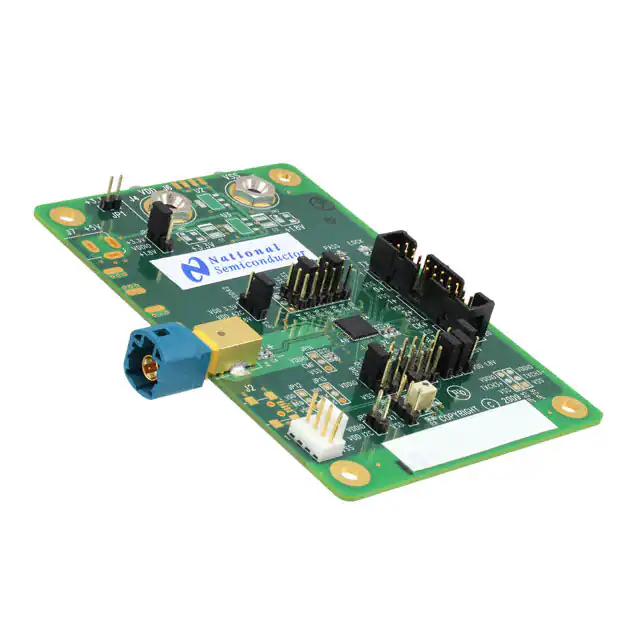
DS90UR908Q-EVK
FPD-Link II to FPD-Link Converter
Evaluation Kit
Rev 0.1
May, 2010
General Description
The DS90UR908Q-EVK converts FPD-link II to FPD-Link. It translates a high-speed serialized interface with an embedded
clock over a single pair to four LVDS data/control streams and one LVDS clock pair. It is backward compatible for operation
with older generation deserializer devices.
The DS90UR908Q-EVK board has a space saving 20-position wall header as the FPD-Link output, and a Rosenberger
Automotive HSD Connector as the input. USB or SMA connectors can also be configured as the input, based on the type of
the cable to be used.
Features
•
•
•
•
•
•
•
•
•
•
•
•
•
•
•
•
•
5 – 65 MHz support (140 Mbps to 1.82 Gbps Serial Link)
5-channel (4 data + 1 clock) FPD-Link driver outputs
AC Coupled STP Interconnect up to 10 meters in length
Integrated input termination
@ Speed link BIST Mode and reporting pin
Optional I2C compatible Serial Control Bus
RGB888 + VS, HS, DE converted from 1 pair
Power down mode minimizes power dissipation
FAST random data lock; no reference clock required
Adjustable input receive equalization
LOCK (real time link status) reporting pin
Low EMI FPD-Link output
SSCG option for lower EMI
1.8V or 3.3V compatible I/O interface
Automotive grade product: AEC-Q100 Grade 2 qualified
>8kV HBM ESD tolerance
Backward compatible mode for operation with older generation devices
Applications
•
•
Automotive Displays for Navigation
Automotive Display for Entertainment
Ordering Information
PART: DS90UR908QSQ
Demo board: DS90UR908Q-EVK
national.com
© National Semiconductor Corporation 2009
1
Printed in U.S.
�Typical Configuration
Quick Start Guide:
1.
2.
3.
4.
Connect 3.3V DC power and ground of the board to the JP1 from the power supply. Connect 1.8V DC power and
ground of the board to the J4 and J5 from the power supply.
Attach an applicable cable (not supplied) to this RX board (DS90UR908) input from a TX board (DS90UR907) output.
From the Video Decoder board, connect a flat cable (not supplied) to the TX board and connect another flat cable
(not supplied) from this RX board to the panel.
Jumpers and switches have been configured at the factory; they should not require any changes for immediate
operation of the board. See text on Configuration Settings and datasheet for more details.
national.com
© National Semiconductor Corporation 2009
2
Printed in U.S.
�Configuration Settings
Component
Name
Function
Power Connections
J7
5V DC
J4
1.8V DC
1.8V VDD Power.
Optional 5V DC Power Jack.
JP1
3.3V DC
3.3V VDD Power.
J5
VSS
Ground.
JP2
VDDIO
Connect to 3.3V or 1.8V.
JP3
VDDA2
Always connect to 1.8V.
-
VDDPC
Always connect to 1.8V.
-
VDDL
Always connect to 1.8V.
-
VDDTXC
Always connect to 3.3V.
Input and Output Connections
20 position wall
header
J8
Automotive HSD
Connector
J1
J9 and J10
SMA Connector
J2
USB Connector
Power Wire in USB
cable through J2
JP12 and JP13
Connect to FPD-Link output.
Connect to FPD-Link II input (default).
Connect to FPD-Link II input.
(When using these connectors, R3 and R4 should be placed with 0Ω resistors, the traces
from R3 and R4 to the J1 should be cut).
Connect to FPD-Link II input.
(When using this connector, P1 should be removed, and R24 and R25 should be placed
with 0Ω resistors)
Connect to VSS is recommended.
Control Connections
JP4
TESTEN
JP5
LF_MODE
JP6
OSSEL
JP7
MAPSEL
JP8
VODSEL
JP9
OEN
JP10
BISTEN
NSC test mode. Always connect it to “L” or leave it unconnected.
Connect to “L” or “H” for the PCLK frequency select. See datasheet for detail information.
Connect to “L” or “H” for the Output State select. See datasheet for detail information.
Connect it to “L” or “H” for the FPD Link mapping select. See datasheet for detail
information.
Connect it to “L” or “H” for the FPD-Link VOD level select. See datasheet for detail
information.
Connect it to “L” or “H” for the Output Enable select. See datasheet for detail information.
Connect it to “H” for the BIST enable mode. See datasheet for detail information.
Connect it to “L” for the power down mode. Connect it to “H” for the enable mode.
See datasheet for detail information.
-
PDB
-
SSC[2:0]
Connect them to “L” or “H” for the SSCG selection.
-
CONFIG
Configuration select. See datasheet for detail information.
Connect JP24 to VSS to have the default device PHY address (h’DC).
Connect JP24 to VR3; then adjust VR3 value to select desired device PHY address. See
datasheet for detail information.
JP24 and VR3
ID[x]
J3 and JP23
I2C Interface
Connect JP23 if the I2C power is not supplied on J6. Otherwise, leave it unconnected.
Others
LED1
PASS
PASS output. “ON” when PASS is “H”
LED2
LOCK
LOCK output. “ON” when LOCK is “H”
JP11, JP25, JP26
Other options
national.com
© National Semiconductor Corporation 2009
Do not connect
3
Printed in U.S.
�Bill of Material
Item
Quantity
Reference
Part
Comments
Digi-Key P/N
Part Number
1
2
C3,C4
0.1uF
CAP CERAMIC .1UF25V X5R 0402
445-4964-1-ND
C1005X5R1E104K
2
1
C5
4.7uF
PCC1731CT-ND
ECJ-0EF1C104Z
3
9
C6,C18,C20,C22,C25,C26,
0.01uF
CAP .1UF 16V CERAMIC Y5V 0402.
CAP CERAMIC .01UF 100V X7R
0603
399-3189-1-ND
C0603C103K1RACTU
0.1uF
CAP .1UF 0% 25V CERAMIC X7R
0603
PCC2277CT-ND
ECJ-1VB1E104K
493-2391-1-ND
F931E226MNC
399-3714-1-ND
T491B225K020AT
399-1249-1-ND
C1206C104K5RACTU
399-3835-1-ND
T494B226M016AT
A26542-ND
87220-2
A26545-ND
87224-3
H2959CT-ND
UX60-MB-5ST
C27,C28,C29
4
10
C7,C17,C19,C21,C23,C24,
C30,C31,C32,C35
5
2
C10,C13
22uF
6
2
C11,C14
2.2uF
7
2
C12,C15
0.1uF
8
3
C16,C33,C34
22uF
9
2
JP1,JP23
2-Pin Header
10
24
JP2,JP3,JP4,JP5,JP6,JP7,
3-Pin Header
CAP TANTALUM 22UF 25V 20%
SMD
CAPACITOR TANT 2.2UF 20V 10%
SMD
CAP .10UF 50V CERAMIC X7R
1206
CAPACITOR TANT 22UF 16V 20%
SMD
CONN HEADER VERT .100 2POS
30AU
CONN HEADER VERT .100 3POS
15AU
JP8,JP9,JP10,JP12,
JP13,JP14,JP15,JP16,JP17,
JP18,JP19,JP20,JP21,JP22,
JP24
11
1
J2
mini USB 5pin
12
1
J3
IDC1X4
13
2
J4,J5
BANANA
14
1
J8
2X10-Pin Header
15
2
J9,J10
SMA
16
1
LED1
0402_orange_LED
17
1
LED2
0603_green_LED
18
2
R1,R2
0 Ohm,0402
19
9
R6,R20,R21,R22,R23,R26,
0 Ohm,0402
CONN RECEPT MINI USB2.0
5POS.
CONN HEADER 4POS .100 VERT
GOLD
BANANA-female (non-insulated)
CONN HEADER 20 POS STRGHT
GOLD.
End Launch Jack Receptacle - Tab
Contact.
LED ORN/CLEAR 610NM 0402
SMD
LED GREEN CLEAR THIN 0603
SMD
RES ZERO OHM 1/16W 5% 0402
SMD.
RES ZERO OHM 1/16W 5% 0402
SMD
WM2702-ND
22-11-2042
J147-ND
108-0740-001
MHC20K-ND
N2520-6002RB
J658-ND
142-0701-851
67-1879-1-ND
SML-LX0402SOC-TR
160-1446-1-ND
LTST-C191KGKT
P0.0JTR-ND
ERJ-2GEJ0R00X
P0.0JTR-ND
ERJ-2GEJ0R00X
P10.0KHCT-ND
ERJ-3EKF1002V
P82.5HCT-ND
RR03P100DCTND
ERJ-3EKF82R5V
P4.7KGCT-ND
ERJ-3GEYJ472V
3224W-1104ECT-ND
3224W-1-104E
R27,R28,R29
20
1
R7
10K
21
2
R10,R11
82.5ohm
22
5
R13,R14,R15,R16,R17
100
23
2
R31,R32
4.7K
24
1
U1
DS90UR908
25
1
VR3
SVR100K
national.com
© National Semiconductor Corporation 2009
RES 10.0K OHM 1/10W 1% 0402
SMD
RES 82.5 OHM 1/10W 1% 0603
SMD
RES 100 OHM 0201 SMD. 1/20W
.5%
RES 4.7K OHM 1/10W 5% 0603
SMD
RR0306P-101-D
DS90UR908
11-Turn Trimming Potentiometer;
Top Adjust
4
Printed in U.S.
�mini USB 5pin
J2
1
2
3
4
5
0.625"
JP12
2
JP24
1
2
3
VR3
IDx
VSS
C4 0.1uF
1
JP23
1
2
0.1uF
VSS
C35
VDDIO
VSS
-
VSS
2
R9
0 Ohm,0402_open
J3
VDDIO
VDD_I2C
VDDA1
P lace R53 and R54 on
the top as the TX board
0 ohm_open
RINR4
0201
LAY OUT NOTE :
100 ohm
diff pair
impedance
traces
0 ohm_open
RIN+
R3
0201
C3 0.1uF
1
2
0 ohm_open
RIN+
R24
0201
0 ohm_open
RINR25
0201
LAY OUT CONNE CTOR
P RIORITY :
1 - J1 (HS D)
2 - J2 (mini B TOP )
3 - J6, J7 (S M A)*
4 - J3 (mini B BOT)
Layout J1, J2, J3, J6, J7
with same spacing
as DS 90UR907
demo board.
LAY OUT NOTE :
100 ohm differential
impedance +/-5%.
LAY OUT NOTE :
Use stripline.
VSS
RIN-_SMA
SMA_open
1
2
3
4
5
J10
VSS
RIN+_SMA
SMA_open
1
2
3
4
5
J9
RIN+_USB
RIN-_USB
VSS
RIN+_USB
RIN-_USB
VSS
RIN-
RIN+
mini B:
component side (BOTTOM)
VSS
9
5
mini USB 5pin_open 4
3
2
1
J11
VSS
VDDIO
mini B:
component side (TOP)
6
J1
JP13
VDDIO
4
3
1
2
HSD_2X2_open
9
1310
1211
8 5
7 6
9
6
8
7
VSS
VSS
LAYOUT NOTE:
Place J2, J3 0.625"
center-to-center of pin #1s.
Footprint on solder side
(bottom).
VSS
RED
5pF 5pF
VSS
C37 C36
VSS
R32
4.7K
0603
VDD_I2C
VSS
VR3
+
SDA
SCL
R31
4.7K
0603
VSS
SDA
SCL
ID[X]
DS90UR908
JP26
VDDIO
3
2
1
1VDDIO
2
3 VSS
JP11
24
23
22
21
20
19
18
17
16
15
28
27
VSS
TXCH0TXCH0+
TXCH1TXCH1+
TXCH2TXCH2+
TXCLKTXCLK+
TXCH3TXCH3+
Place close to JP17 Pin2 (For 124 option)
0 Ohm,0402_open
R30
4
5
12
40
41
42
PASS
LOCK
JP14
3
2
1
RIN+
RINCMF
JP15
3
2
1
CMF
JP16
3
2
1
U1
JP17
3
2
1
R5
VSS
2
4.7uF
C5
1
1K Ohm,0402_open
CMF
R18
0 ohm_open
0201
VDDIO
3
2
1
5
Printed in U.S.
Date:
Size
B
Title
1
3
5
TxCH1+
7
9
TxCH2+
11
13
TxCLK+ 15
17
19
TxCH3+
TxCH0+
J8
Monday , August 10, 2009
Document Number
Rx Demo Board
Rx Demo Board - Deserializer
Place R70 and R71 on
the top layer
VSS
VSS
R19
0 ohm_open
0201
JP25
R17
100
0201
R16
100
0201
R15
100
0201
R14
100
0201
R13
100
0201
2
4
6
8
10
12
14
16
18
20
Sheet
TxCH3-
TxCLK-
TxCH2-
TxCH1-
TxCH0-
2
VSS
of
3
Rev
A
Place JP22, JP23, JP32 together, with matched trace length 50 ohm
Place JP19, JP20, JP21 together, with matched trace length 50 ohm
VSS
0402_orange_LED LED1
R1
2
1
0603_green_LED LED2
0 Ohm,0402
R2
2
1
0 Ohm,0402
JP18
3
2
1
C33
22uF
JP10
JP9
JP8
JP7
JP6
JP5
JP4
JP19
3
2
1
PDB
SSC[0]
SSC[1]
SSC[2]
1
2
3
2
1
CONFG[0]
CONFG[1]
VDDL1
VDDP
VDDTX
VDDIO
VDDL2
VDDA1
VDDA2
VDDSC1
VDDSC2
+
3
2
1
6
8
13
25
31
38
43
46
47
VDDL1
VDDP
VDDTX
VDDIO
VDDL2
VDDA1
VDDA2
VDDSC1
VDDSC2
7
8
SVR100K
3
2
1
VDDL1
VDDP
VDDTX
VDDIO
VDDL2
VDDA1
VDDA2
VDDSC1
VDDSC2
1
RED 2
3
BLK
1
2
3
BLK
R7
10K
100K_open R8
1
2
3
4
1
CW
3
3
2
1
1
2
3
7
3
2
1
10
11
3
2
1
37
36
35
34
33
30
29
3
2
1
TESTEN
LF_MODE
OSSEL
MAPSEL
VODSEL
BISTM
BISTEN
© National Semiconductor Corporation 2009
GND
GND
GND
GND
GND
GND
GND
GND
DAP
national.com
9
14
26
32
39
44
45
48
49
VD DL 1
VD DP
VD DT X
VD DIO
VD DL 2
VD DA1
VD DA2
VD DSC1
VD DSC2
Schematics
�1
BANANA
J5
BANANA
1
C14 +
2.2uF
2
1
C13 +
22uF
2
1
3
5
7
OPTION AL
5V IN PU T POW ER
C ON N EC TOR
1
2
3
CONN JACK PWR_open
J7
2x4 pin Jumper_open
VSS
J6
2
4
6
8
0.1uF
C15 +
1
VSS
+
VSS
VD D
VDD3.3V
VSS
+ C1
+
VSS
VDD
VDD
VDD
10uF_open
10uF_open
C2
3.3V
10uF_open
10uF_open
C8
+ C9
VDD1.8V
2
VDD
1
1
1
2
R10
82.5ohm
3
2
1
INPUT
Tab/Vout OUTPUT
ADJ/GND
4
R11
82.5ohm
2
1
2
1
2
U2
U3
2
VSS
R28
0 Ohm,0402
VSS
R26
0 Ohm,0402
VSS
R21
0 Ohm,0402
CW
3
22uF
C21
C24
1
VSS
VDD3.3V
VSS
Place near pin 47 of U1
VD D SC 2
Place near pin 46 of U1
VD D SC 1
C16
22uF
Place near pin 38 of U1
VD D A 1
0.1uF
2.2uF
VDDA1
C12 +
VDDSC2
0.01uF 0.1uF
C29
+
VDDSC1
C30
0.01uF 0.1uF
C26
0.01uF 0.1uF
C22
JP1
C10 +
C11 +
OPTIONAL Exte rnal 3.3V input.
OPTION AL
5V to 3.3V
IN PU T POW ER
R EGU LATOR
VR1
R12 1
100ohm_open
SVR100_open
VSS
OPTIONAL
5V to 1.8V
INPUT POWER
REGULATOR
SVR100_open
VSS
VR2
CW 3
1
LM1117IMP-ADJ/SOT223_open
LM1117IMP-ADJ/SOT223_open
3
2
1
INPUT
Tab/Vout OUTPUT
ADJ/GND
4
2
J4
1
2
1
2
!!!WARNING!!!
Input power thru J5 OR J4 OR JP3 OR J9
ONLY!!
Input power thru only one connector!!
VSS
1
2
1.8V INPUT
POWER
CONNECTOR
1
2
1
2
© National Semiconductor Corporation 2009
2
national.com
6
Printed in U.S.
C34
22uF
VSS
+
C19
0.01uF 0.1uF
C20
VSS
C17
0.01uF 0.1uF
C18
VDDIO=VDD (1.8V)
R23
0 Ohm,0402
VDDI
C32
0.01uF 0.1uF
C28
VDDIO=3.3V (externa l )
JP2
VSS
R20
0 Ohm,0402
VSS
R29
0 Ohm,0402
VDDIO=VDD (1.8V)
VDDIO=3.3V (externa l)
JP21
VDD3.3V 1
2
VDD
3
VDD3.3V 1
2
VDD
3
VD D L1
VD D L2
VD D IO
Place near pin 25 of U1
VDDIO
Place near pin 31 of U1
VDDL2
Place near pin 6 of U1
VDDL1
VSS
R27
0 Ohm,0402
C31
Date:
Size
Title
C7
VD D P
Monday , August 10, 2009
Document Number
Rx Demo Board
VD D TX
Sheet
4
Place near pin 13 of U1
VDDTX
Place near pin 8 of U1
VDDP
0.01uF 0.1uF
C6
Rx Demo Board - Power and Decoupling
0.01uF 0.1uF
C27
VSS
R6
0 Ohm,0402
VDDIO=VDD (1.8V)
VDDTXc
VDDIO=VDD (1.8V)
VD D A 2
Place near pin 43 of U1
VDDA2
VDDIO=3.3V (externa l )
JP22
VDDIO=3.3V (externa l )
JP20
VDDPc
VDD3.3V 1
2
VDD
3
C23
0.01uF 0.1uF
C25
VDD3.3V 1
2
VDD
3
VSS
R22
0 Ohm,0402
VDDIO=VDD (1.8V)
VDDIO=3.3V (externa l )
JP3
VDDA2c
VDD3.3V 1
2
VDD
3
of
4
Rev
A
�Reference Layout
Top Layer
national.com
© National Semiconductor Corporation 2009
Bottom Layer
7
Printed in U.S.
�IMPORTANT NOTICE
Texas Instruments Incorporated and its subsidiaries (TI) reserve the right to make corrections, modifications, enhancements, improvements,
and other changes to its products and services at any time and to discontinue any product or service without notice. Customers should
obtain the latest relevant information before placing orders and should verify that such information is current and complete. All products are
sold subject to TI’s terms and conditions of sale supplied at the time of order acknowledgment.
TI warrants performance of its hardware products to the specifications applicable at the time of sale in accordance with TI’s standard
warranty. Testing and other quality control techniques are used to the extent TI deems necessary to support this warranty. Except where
mandated by government requirements, testing of all parameters of each product is not necessarily performed.
TI assumes no liability for applications assistance or customer product design. Customers are responsible for their products and
applications using TI components. To minimize the risks associated with customer products and applications, customers should provide
adequate design and operating safeguards.
TI does not warrant or represent that any license, either express or implied, is granted under any TI patent right, copyright, mask work right,
or other TI intellectual property right relating to any combination, machine, or process in which TI products or services are used. Information
published by TI regarding third-party products or services does not constitute a license from TI to use such products or services or a
warranty or endorsement thereof. Use of such information may require a license from a third party under the patents or other intellectual
property of the third party, or a license from TI under the patents or other intellectual property of TI.
Reproduction of TI information in TI data books or data sheets is permissible only if reproduction is without alteration and is accompanied
by all associated warranties, conditions, limitations, and notices. Reproduction of this information with alteration is an unfair and deceptive
business practice. TI is not responsible or liable for such altered documentation. Information of third parties may be subject to additional
restrictions.
Resale of TI products or services with statements different from or beyond the parameters stated by TI for that product or service voids all
express and any implied warranties for the associated TI product or service and is an unfair and deceptive business practice. TI is not
responsible or liable for any such statements.
TI products are not authorized for use in safety-critical applications (such as life support) where a failure of the TI product would reasonably
be expected to cause severe personal injury or death, unless officers of the parties have executed an agreement specifically governing
such use. Buyers represent that they have all necessary expertise in the safety and regulatory ramifications of their applications, and
acknowledge and agree that they are solely responsible for all legal, regulatory and safety-related requirements concerning their products
and any use of TI products in such safety-critical applications, notwithstanding any applications-related information or support that may be
provided by TI. Further, Buyers must fully indemnify TI and its representatives against any damages arising out of the use of TI products in
such safety-critical applications.
TI products are neither designed nor intended for use in military/aerospace applications or environments unless the TI products are
specifically designated by TI as military-grade or "enhanced plastic." Only products designated by TI as military-grade meet military
specifications. Buyers acknowledge and agree that any such use of TI products which TI has not designated as military-grade is solely at
the Buyer's risk, and that they are solely responsible for compliance with all legal and regulatory requirements in connection with such use.
TI products are neither designed nor intended for use in automotive applications or environments unless the specific TI products are
designated by TI as compliant with ISO/TS 16949 requirements. Buyers acknowledge and agree that, if they use any non-designated
products in automotive applications, TI will not be responsible for any failure to meet such requirements.
Following are URLs where you can obtain information on other Texas Instruments products and application solutions:
Products
Applications
Audio
www.ti.com/audio
Automotive and Transportation www.ti.com/automotive
Amplifiers
amplifier.ti.com
Communications and Telecom www.ti.com/communications
Data Converters
dataconverter.ti.com
Computers and Peripherals
www.ti.com/computers
DLP® Products
www.dlp.com
Consumer Electronics
www.ti.com/consumer-apps
DSP
dsp.ti.com
Energy and Lighting
www.ti.com/energy
Clocks and Timers
www.ti.com/clocks
Industrial
www.ti.com/industrial
Interface
interface.ti.com
Medical
www.ti.com/medical
Logic
logic.ti.com
Security
www.ti.com/security
Power Mgmt
power.ti.com
Space, Avionics and Defense
www.ti.com/space-avionics-defense
Microcontrollers
microcontroller.ti.com
Video and Imaging
www.ti.com/video
RFID
www.ti-rfid.com
OMAP Mobile Processors
www.ti.com/omap
Wireless Connectivity
www.ti.com/wirelessconnectivity
TI E2E Community Home Page
e2e.ti.com
Mailing Address: Texas Instruments, Post Office Box 655303, Dallas, Texas 75265
Copyright © 2012, Texas Instruments Incorporated
�


 工商网监
湘ICP备2023018690号
工商网监
湘ICP备2023018690号
