DS90UR910QEVM User’s Guide
User's Guide
Literature Number: SNLU143
September 2013
�User's Guide
SNLU143 – September 2013
DS90UR910QEVM Evaluation Kit
The DS90UR910QEVM converts FPD-Link II to MIPI CSI-2. This kit will demonstrate the functionality and
operation of the DS90UR910Q. The DS90UR910Q is an interface bridge chip that recovers data from the
FPD-Link II serial bit stream and converts into a Camera Serial Interface (CSI-2) format compatible with
Mobile Industry Processor Interface (MIPI) specifications. It recovers the 24- or 18-bit RGB data and 3
video sync-signals from the serial bit stream compatible to FPD-Link II serializers.
The recovered data is packetized and serialized over two data lanes strobed by a half-rate serial clock
compliant with the MIPI DPHY / CSI-2 specifications, each running up to 900 Mbps. The FPD-Link II
receiver supports pixel clocks of up to 75 MHz. The CSI-2 output serial bus greatly reduces the
interconnect and signal count to a graphic processing unit (GPU) and eases system designs for video
streams from multiple automotive driver assist cameras.
NOTE: The demo board is not intended for EMI testing. The demo board was designed for
easy accessibility to device pins with tap points for monitoring or applying signals,
additional pads for termination, and multiple connector options.
Topic
1
2
3
4
5
6
7
2
...........................................................................................................................
Page
DS90UR910QEVM ............................................................................................... 3
Quick Start Guide ................................................................................................ 5
References ......................................................................................................... 9
Bill of Materials for DS90UR910QEVM: ................................................................. 10
Schematic for DS90UR910QEVM: ........................................................................ 12
EVM Layout ...................................................................................................... 14
EVM PCB Stackup ............................................................................................. 16
DS90UR910QEVM Evaluation Kit
SNLU143 – September 2013
Submit Documentation Feedback
Copyright © 2013, Texas Instruments Incorporated
�DS90UR910QEVM
www.ti.com
1
DS90UR910QEVM
The Texas Instruments DS90UR910QEVM evaluation module (EVM) helps system designers evaluate the
operation and performance of the DS90UR910Q 10 - 75 MHz 24-bit Color FPD-Link II to CSI-2 Converter.
1.1
Features
•
•
•
•
•
•
•
•
•
•
•
•
•
•
•
•
•
1.2
1.3
10 – 75 MHz PCLK support (280 Mbps – 2.10 Gbps FPD-Link II linerate)
Compatible to DC balanced, AC coupled for FPD-Link II serial bit stream
Capable to recover data up to 10 meters STP cable
MIPI D-PHY modules conform to v1.00.00
Compatible with MIPI CSI-2 Version 1.01
Supports data rate up to 900Mbps per data lane, with two lanes
Video stream packet formats: RGB888
Continuous and Non-Continuous Clocking Mode
Ultra low power, escape, high speed, and control modes support
Integrated input terminations and adjustable receive equalization
Fast random lock; no reference clock required
CCI/I2C compatible control bus
@Speed BIST and reporting pin
Single +1.8V power supply
1.8V or 3.3V compatible LVCMOS I/O interface
Automotive grade product: AEC-Q100 Grade 2 qualified
8 kV ISO 10605 ESD Rating
Ordering Information
Reference
DEVICE ID
DEVICE PACKAGE
U1
DS90UR910SQE
WQFN40
System Requirements
In order to demonstrate, the following is required:
1. FPD-Link II compatible Serializer
• DS90UR905Q, DS90UR241Q, DS90C241Q, DS90UR907Q, DS99R421Q
• DS90UH/UB/925/927Q FPD-Link III serializers in backward compatibility mode
2. Video source
3. Optional I2C controller
4. Power supply for 1.8V (required) and 3.3V (optional)
1.4
Contents of the Demo Evaluation Kit
•
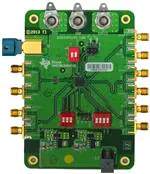
1.5
One EVM board with the DS90UR910Q
Applications Diagram
Figure 1 and Figure 2 below illustrate the use of the chipset in a display application.
SNLU143 – September 2013
Submit Documentation Feedback
DS90UR910QEVM Evaluation Kit
Copyright © 2013, Texas Instruments Incorporated
3
�DS90UR910QEVM
www.ti.com
VDD
1.8V
VDDIO
VDD
(1.8V or 3.3V) 1.8V
VDDIO
(1.8V or 3.3V)
CSI-2
R[7:0]
G[7:0]
0.1 µF
0.1 µF
DATA1±
DOUT+
RIN+
B[7:0]
Video
sources
DATA0±
0.1 µF
HS
Graphic
Processor
0.1 µF
DOUT-
VS
DE
PCLK
RIN-
CLK±
Application
Processor
FPD-Link II
1 pair 100�673
DS90UR910Q
Converter
DS90UR905Q
Serializer
PDB
EQ[3:1]
CONFIG[1:0]
SCL
RFB
SDA
VODSEL
DeEmph
ID[x]
SCL
SDA
LOCK
CONFIG[1:0]
BISTEN
Display
PDB
ID[1:0]
BISTEN
PASS
Control
pins
DAP GND
DAP
Figure 1. Applications Diagram
1.6
Typical Configuration
Video Processor Board
(Video Data + Ctrl)
Video
Processor
FPD-Link II
Serializer
PCLK
FPD-Link II
Cluster, Head Unit
DS90UR910Q
Converter
(I2C_CTRL)
(MIPI CSI-2)
Application
Processor
Display
Figure 2. Diagram
4
DS90UR910QEVM Evaluation Kit
SNLU143 – September 2013
Submit Documentation Feedback
Copyright © 2013, Texas Instruments Incorporated
�Quick Start Guide
www.ti.com
2
Quick Start Guide
1. Connect header JP3 to I2C host controller for register programming (optional)
2. Configure switches S1, S2 and S3 to set device’s operating modes
3. Connect J1, J2 (RIN+, RIN-) to FPD-Link serial bit stream from an external DS90UR905, DS90Ux925,
or compatible FPD-Link II serializer.
4. Connect CSI-2 output signals (J4-8, J10) to GPU
5. Provide power to board on VDD (1.8V), GND (Ground), and VDDIO (1.8V or 3.3V)
• Optional +5VDC power supply on J11
6. Look for the LED D1 to light up on the board. If the LED is lit and stable, then the DS90UR910Q is
LOCKED to the FPD-Link II serial stream. LED D2 will be lit when a valid display timing is detected.
7. For details of pin-names and pin-functions, please refer to the DS90UR910 datasheet
P6, P8, P4 f
1.8V
+5%
GND
1.8V+5% OR
3.3V+10%
c FPD-LINK II INPUTS
d LVCMOS I/O
e FUNCTION CONTROLS
f POWER SUPPLY
g
CSI-2 OUTPUTS SIGNALS
h I2C/CCI BUS
i CMLOUT OUTPUTS
dJP4
J1, J2, P1 c
S1, S2, S3 e
J3, J9 i
g J4-J8, J10
JP3 h
Figure 3. Evaluation Board Connections
SNLU143 – September 2013
Submit Documentation Feedback
DS90UR910QEVM Evaluation Kit
Copyright © 2013, Texas Instruments Incorporated
5
�Quick Start Guide
2.1
www.ti.com
Demo Board Connections
Table 1. Power Supply Connection
Reference
Signal
Description
P4
VDDIO
1.8V ±5% OR 3.3V ±10%
P5
GND
Ground
P6
VDD
1.8V ±5%
J11 (Optional)
+5V
Single main +5V (0.5A) power connector that supplies power to the entire
board. Short jumpers JP7 and JP6 for 1.8V and 3.3V on board regulator
power supplies respectively.
Table 2. CSI-2 Output Signals
Reference
Signal
J4
DATA1+
Description
Non-inverting data output of DPHY Lane 1
J5
DATA1-
Inverting data output of DPHY Lane 1
J6
DATA0+
Non-inverting data output of DPHY Lane 0
J7
DATA0-
Inverting data output of DPHY Lane 0
J8
CLK+
Non-inverting half-rate DPHY clock lane
J10
CLK-
Inverting half-rate DPHY clock lane
Table 3. FPD-Link II Input Signal
Reference
Signal
Description
J1
RIN+
SMA connector
J2
RIN-
SMA connector
P1 (Optional)
RIN+/-
HSD connector
Populate C17 and C18 to use P1 connector.
Table 4. I2C/CCI Interface Header
Reference
Signal
JP3.1
VDDI2C
Description
JP3.2
SCL
I2C/CCI SCL
JP3.3
SDA
I2C/CCI SDA
JP3.4
GND
Ground
I2C/CCI VDDIO
Table 5. Control Status
Reference
Signal
Description
JP4.1
LOCK
LOCK = 1, PLL acquired lock to the reference clock input
LOCK = 0, PLL is unlocked
JP4.3
PASS
PASS = 1: No fault detected on input display timing.
PASS = 0: Indicates an error condition or corruption in display video timing.
JP4.5
GPIO
General Purpose I/O
Table 6. CMLOUT Output Signals
6
Reference
Signal
J3
CMLOUT+
Description
SMA connector
J9
CMLOUT-
SMA connector
DS90UR910QEVM Evaluation Kit
SNLU143 – September 2013
Submit Documentation Feedback
Copyright © 2013, Texas Instruments Incorporated
�Quick Start Guide
www.ti.com
Table 7. EQ Setting SW-DIP3 – S2
Reference
Signal
Description
Receiver Equalization Configuration
S2.1
EQ1
S2.2
EQ2
S2.3
EQ3
EQ[3:1]
EQ Boost
001
~3 dB
010
~4.5 dB
011
~6 dB
100
~7.5 dB
101
~9 dB
110
~10.5 dB
111
~12 dB
000
OFF* (Default)
Table 8. Config/ID Setting SW-DIP4 – S1
Reference
Signal
Description
S1.1
CONFIG0
Configuration Modes
S1.2
CONFIG1
CONFIG1
CONFIG0
L (Default)
L (Default)
DS90UR905Q/907Q, DS90Ux925Q
MODE
L
H
DS90UR905Q/907Q, DS90Ux925Q
H
L
DS90UR241Q, DS99R421Q
H
H
DS90C241Q
CCI/I2C Slave Address Select
S1.3
ID0
S1.4
ID1
ID1
ID0
SLAVE ADDRESS
L (Default)
L (Default)
0x3C'h (0x78'h
很抱歉,暂时无法提供与“DS90UR910QEVM”相匹配的价格&库存,您可以联系我们找货
免费人工找货- 国内价格 香港价格
- 1+4991.620281+645.55223