DS92LV010A
www.ti.com
SNLS007E – MAY 1998 – REVISED APRIL 2013
DS92LV010A Bus LVDS 3.3/5.0V Single Transceiver
Check for Samples: DS92LV010A
FEATURES
DESCRIPTION
•
•
•
•
•
•
•
•
•
The DS92LV010A is one in a series of transceivers
designed specifically for the high speed, low power
proprietary bus backplane interfaces. The device
operates from a single 3.3V or 5.0V power supply
and includes one differential line driver and one
receiver. To minimize bus loading the driver outputs
and receiver inputs are internally connected. The
logic interface provides maximum flexibility as 4
separate lines are provided (DIN, DE, RE, and
ROUT). The device also features flow through which
allows easy PCB routing for short stubs between the
bus pins and the connector. The driver has 10 mA
drive capability, allowing it to drive heavily loaded
backplanes, with impedance as low as 27 Ohms.
1
2
•
•
•
Bus LVDS Signaling (BLVDS)
Designed for Double Termination Applications
Balanced Output Impedance
Lite Bus Loading 5pF Typical
Glitch Free Power Up/Down (Driver Disabled)
3.3V or 5.0V Operation
±1V Common Mode Range
±100mV Receiver Sensitivity
High Signaling Rate Capability (Above 100
Mbps)
Low Power CMOS Design
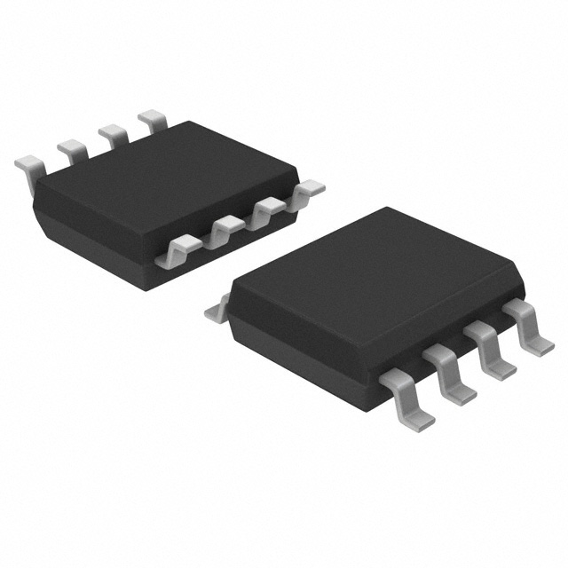
Product Offered in 8 Lead SOIC Package
Industrial Temperature Range Operation
The driver translates between TTL levels (singleended) to Low Voltage Differential Signaling levels.
This allows for high speed operation, while
consuming minimal power with reduced EMI. In
addition the differential signaling provides common
mode noise rejection of ±1V.
The receiver threshold is ±100mV over a ±1V
common mode range and translates the low voltage
differential levels to standard (CMOS/TTL) levels.
CONNECTION DIAGRAM
Figure 1. SOIC Package
See Package Number D0008A
BLOCK DIAGRAM
Figure 2.
1
2
Please be aware that an important notice concerning availability, standard warranty, and use in critical applications of
Texas Instruments semiconductor products and disclaimers thereto appears at the end of this data sheet.
All trademarks are the property of their respective owners.
PRODUCTION DATA information is current as of publication date.
Products conform to specifications per the terms of the Texas
Instruments standard warranty. Production processing does not
necessarily include testing of all parameters.
Copyright © 1998–2013, Texas Instruments Incorporated
�DS92LV010A
SNLS007E – MAY 1998 – REVISED APRIL 2013
www.ti.com
These devices have limited built-in ESD protection. The leads should be shorted together or the device placed in conductive foam
during storage or handling to prevent electrostatic damage to the MOS gates.
ABSOLUTE MAXIMUM RATINGS
(1) (2) (3)
Supply Voltage (VCC)
6.0V
Enable Input Voltage (DE, RE)
−0.3V to (VCC + 0.3V)
Driver Input Voltage (DIN)
−0.3V to (VCC + 0.3V)
Receiver Output Voltage
−0.3V to (VCC + 0.3V)
(ROUT)
−0.3V to + 3.9V
Bus Pin Voltage (DO/RI±)
Driver Short Circuit Current
Continuous
ESD (HBM 1.5 kΩ, 100 pF)
Maximum Package Power Dissipation at 25°C
>2.0 kV
SOIC
1025 mW
Derate SOIC Package
8.2 mW/°C
Junction Temperature
+150°C
−65°C to +150°C
Storage Temperature Range
Lead Temperature
(1)
(2)
(3)
(Soldering, 4 sec.)
260°C
All currents into device pins are positive; all currents out of device pins are negative. All voltages are referenced to device ground except
VOD, VID, VTH and VTL unless otherwise specified.
Absolute Maximum Ratings are these beyond which the safety of the device cannot be ensured. They are not meant to imply that the
device should be operated at these limits. The table of “Electrical Characteristics” provides conditions for actual device operation.
If Military/Aerospace specified devices are required, please contact the Texas Instruments Sales Office/ Distributors for availability and
specifications.
RECOMMENDED OPERATING CONDITIONS
Min
Max
Units
Supply Voltage (VCC), or
3.0
3.6
V
Supply Voltage (VCC)
4.5
5.5
V
Receiver Input Voltage
0.0
2.9
V
Operating Free Air Temperature
−40
+85
°C
2
Submit Documentation Feedback
Copyright © 1998–2013, Texas Instruments Incorporated
Product Folder Links: DS92LV010A
�DS92LV010A
www.ti.com
SNLS007E – MAY 1998 – REVISED APRIL 2013
(1) (2)
3.3V DC ELECTRICAL CHARACTERISTICS
TA = −40°C to +85°C unless otherwise noted, VCC = 3.3V ± 0.3V
Parameter
Test Conditions
VOD
Output Differential Voltage
ΔVOD
VOD Magnitude Change
RL = 27Ω, See Figure 3
VOS
Offset Voltage
ΔVOS
Offset Magnitude Change
IOSD
Output Short Circuit Current
VO = 0V, DE = VCC
VOH
Voltage Output High
VID = +100 mV
Pin
DO+/RI+,
DO−/RI−
Min
Typ
Max
Units
140
250
360
mV
3
30
mV
1.25
1.65
V
5
50
mV
−12
−20
mA
1
I OH = −400 µA
2.8
3
V
Inputs Open
2.8
3
V
Inputs Shorted
2.8
3
V
Inputs Terminated, RL = 27Ω
2.8
3
VOL
Voltage Output Low
IOL = 2.0 mA, VID = −100 mV
IOS
Output Short Circuit Current
VOUT = 0V, VID = +100 mV
VTH
Input Threshold High
DE = 0V
VTL
Input Threshold Low
IIN
Input Current
VIH
Minimum Input High Voltage
VIL
Maximum Input Low Voltage
IIH
Input High Current
VIN = VCC or 2.4V
IIL
Input Low Current
VIN = GND or 0.4V
VCL
Input Diode Clamp Voltage
ICLAMP = −18 mA
ICCD
Power Supply Current
DE = RE = VCC , RL = 27Ω
R OUT
0.1
−5
DO+/RI+,
DO−/RI−
DE = 0V, VIN = +2.4V, or 0V
VCC = 0V, VIN = +2.4V, or 0V
DIN,
DE,RE
V
−85
mA
+100
mV
−100
mV
−20
±1
−20
±1
+20
µA
+20
µA
2.0
VCC
V
GND
0.8
V
±1
±10
µA
±1
±10
µA
−1.5
−0.8
V
13
20
mA
ICCR
DE = RE = 0V
5
8
mA
ICCZ
DE = 0V, RE = VCC
3
7.5
mA
ICC
DE = VCC, RE = 0V, RL = 27Ω
16
22
mA
Coutput
(1)
(2)
Capacitance @ BUS Pins
V CC
−35
V
0.4
DO+/RI+,
DO−/RI−
5
pF
All currents into device pins are positive; all currents out of device pins are negative. All voltages are referenced to device ground except
VOD, VID, VTH and VTL unless otherwise specified.
All typicals are given for VCC = +3.3V or 5.0 V and TA = +25°C, unless otherwise stated.
Submit Documentation Feedback
Copyright © 1998–2013, Texas Instruments Incorporated
Product Folder Links: DS92LV010A
3
�DS92LV010A
SNLS007E – MAY 1998 – REVISED APRIL 2013
www.ti.com
5V DC ELECTRICAL CHARACTERISTICS
(1) (2)
TA = −40°C to +85°C unless otherwise noted, VCC = 5.0V ± 0.5V
Parameter
Test Conditions
VOD
Output Differential Voltage
ΔVOD
VOD Magnitude Change
VOS
Offset Voltage
ΔVOS
Offset Magnitude Change
IOSD
Output Short Circuit Current
VO = 0V, DE = VCC
VOH
Voltage Output High
VID = +100 mV
Pin
RL = 27Ω, See Figure 3
DO+/RI+,
DO−/RI−
Min
Typ
Max
Units
145
270
390
mV
3
30
mV
1.35
1.65
V
5
50
mV
−12
−20
mA
1
IOH = −400 µA
4.3
5.0
V
Inputs Open
4.3
5.0
V
Inputs Shorted
4.3
5.0
V
Inputs Terminated, RL = 27Ω
4.3
5.0
VOL
Voltage Output Low
IOL = 2.0 mA, VID = −100 mV
IOS
Output Short Circuit Current
VOUT = 0V, VID = +100 mV
VTH
Input Threshold High
DE = 0V
VTL
Input Threshold Low
IIN
Input Current
VIH
Minimum Input High Voltage
VIL
Maximum Input Low Voltage
IIH
Input High Current
VIN = VCC or 2.4V
IIL
Input Low Current
VIN = GND or 0.4V
VCL
Input Diode Clamp Voltage
ICLAMP = −18 mA
ICCD
Power Supply Current
DE = RE = VCC, RL = 27Ω
ROUT
−35
DO+/RI+,
DO−/RI−
DE = 0V, VIN = +2.4V, or 0V
VCC = 0V, VIN = +2.4V, or 0V
DIN, DE,
RE
0.4
V
−90
−130
mA
+100
mV
−100
mV
−20
±1
−20
±1
+20
µA
+20
µA
2.0
VCC
V
GND
0.8
V
±1
±10
µA
±1
±10
µA
−1.5
−0.8
V
17
25
mA
ICCR
DE = RE = 0V
6
10
mA
ICCZ
DE = 0V, RE = VCC
3
8
mA
ICC
DE = VCC, RE = 0V, RL = 27Ω
20
25
mA
Coutput
(1)
(2)
4
Capacitance @ BUS Pins
V CC
V
0.1
DO+/RI+,
DO−/RI−
5
pF
All currents into device pins are positive; all currents out of device pins are negative. All voltages are referenced to device ground except
VOD, VID, VTH and VTL unless otherwise specified.
All typicals are given for VCC = +3.3V or 5.0 V and TA = +25°C, unless otherwise stated.
Submit Documentation Feedback
Copyright © 1998–2013, Texas Instruments Incorporated
Product Folder Links: DS92LV010A
�DS92LV010A
www.ti.com
SNLS007E – MAY 1998 – REVISED APRIL 2013
3.3V AC ELECTRICAL CHARACTERISTICS
(1)
TA = −40°C to +85°C, VCC = 3.3V ± 0.3V
Parameter
Test Conditions
Min
Typ
Max
Units
1.0
3.0
5.0
ns
1.0
2.8
5.0
ns
DIFFERENTIAL DRIVER TIMING REQUIREMENTS
tPHLD
Differential Prop. Delay High to
Low
RL = 27Ω, See Figure 4 and Figure 5
CL = 10 pF
tPLHD
Differential Prop. Delay Low to
High
tSKD
Differential SKEW |t PHLD tPLHD|
0.2
1.0
ns
tTLH
Transition Time Low to High
0.3
2.0
ns
tTHL
Transition Time High to Low
tPHZ
Disable Time High to Z
tPLZ
Disable Time Low to Z
tPZH
tPZL
0.3
2.0
ns
0.5
4.5
9.0
ns
0.5
5.0
10.0
ns
Enable Time Z to High
2.0
5.0
7.0
ns
Enable Time Z to Low
1.0
4.5
9.0
ns
2.5
5.0
12.0
ns
2.5
5.5
10.0
ns
RL = 27Ω, See Figure 6 and Figure 7
CL = 10 pF
DIFFERENTIAL RECEIVER TIMING REQUIREMENTS
tPHLD
Differential Prop. Delay High to
Low
tPLHD
Differential Prop. Delay Low to
High
tSKD
Differential SKEW |t PHLD tPLHD|
0.5
2.0
ns
tr
Rise Time
1.5
4.0
ns
tf
Fall Time
tPHZ
Disable Time High to Z
tPLZ
Disable Time Low to Z
tPZH
tPZL
(1)
(2)
See Figure 8 and Figure 9
CL = 10 pF
1.5
4.0
ns
2.0
4.0
6.0
ns
2.0
5.0
7.0
ns
Enable Time Z to High
2.0
7.0
13.0
ns
Enable Time Z to Low
2.0
6.0
10.0
ns
RL = 500Ω, See Figure 10 and Figure 11
CL = 10 pF (2)
Generator waveforms for all tests unless otherwise specified: f = 1MHz, ZO = 50Ω, tr, tf ≤ 6.0ns (0%–100%) on control pins and ≤ 1.0ns
for RI inputs.
For receiver tri-state delays, the switch is set to VCC for tPZL, and tPLZ and to GND for tPZH, and tPHZ.
Submit Documentation Feedback
Copyright © 1998–2013, Texas Instruments Incorporated
Product Folder Links: DS92LV010A
5
�DS92LV010A
SNLS007E – MAY 1998 – REVISED APRIL 2013
www.ti.com
5V AC ELECTRICAL CHARACTERISTICS
(1)
TA = −40°C to +85°C, VCC = 5.0V ± 0.5V
Parameter
Test Conditions
Min
Typ
Max
Units
0.5
2.7
4.5
ns
0.5
2.5
4.5
ns
DIFFERENTIAL DRIVER TIMING REQUIREMENTS
tPHLD
Differential Prop. Delay High to
Low
RL = 27Ω, See Figure 4 and Figure 5
CL = 10 pF
tPLHD
Differential Prop. Delay Low to
High
tSKD
Differential SKEW |t PHLD tPLHD|
0.2
1.0
ns
tTLH
Transition Time Low to High
0.3
2.0
ns
tTHL
Transition Time High to Low
tPHZ
Disable Time High to Z
tPLZ
Disable Time Low to Z
tPZH
tPZL
0.3
2.0
ns
0.5
3.0
7.0
ns
0.5
5.0
10.0
ns
Enable Time Z to High
2.0
4.0
7.0
ns
Enable Time Z to Low
1.0
4.0
9.0
ns
2.5
5.0
12.0
ns
2.5
4.6
10.0
ns
RL = 27Ω, See Figure 6 and Figure 7
CL = 10 pF
DIFFERENTIAL RECEIVER TIMING REQUIREMENTS
tPHLD
Differential Prop. Delay High to
Low
tPLHD
Differential Prop. Delay Low to
High
tSKD
Differential SKEW |t PHLD tPLHD|
0.4
2.0
ns
tr
Rise Time
1.2
2.5
ns
tf
Fall Time
tPHZ
Disable Time High to Z
tPLZ
Disable Time Low to Z
tPZH
tPZL
(1)
(2)
See Figure 8 and Figure 9
CL = 10 pF
1.2
2.5
ns
2.0
4.0
6.0
ns
2.0
4.0
6.0
ns
Enable Time Z to High
2.0
5.0
9.0
ns
Enable Time Z to Low
2.0
5.0
7.0
ns
RL = 500Ω, See Figure 10 and Figure 11
CL = 10 pF (2)
Generator waveforms for all tests unless otherwise specified: f = 1MHz, ZO = 50Ω, tr, tf ≤ 6.0ns (0%–100%) on control pins and ≤ 1.0ns
for RI inputs.
For receiver tri-state delays, the switch is set to VCC for tPZL, and tPLZ and to GND for tPZH, and tPHZ.
TEST CIRCUITS AND TIMING WAVEFORMS
Figure 3. Differential Driver DC Test Circuit
6
Submit Documentation Feedback
Copyright © 1998–2013, Texas Instruments Incorporated
Product Folder Links: DS92LV010A
�DS92LV010A
www.ti.com
SNLS007E – MAY 1998 – REVISED APRIL 2013
Figure 4. Differential Driver Propagation Delay and Transition Time Test Circuit
3V
1.5V
DIN
1.5V
0V
tPHLD
tPLHD
DO0V
DO+, DO-
Differential
0V
DO+
(DO+) - (DO-)
80%
80%
0V
20%
20%
tTLH
tTHL
VDIFF = (DO+) - (DO-)
Figure 5. Differential Driver Propagation Delay and Transition Time Waveforms
Figure 6. Driver TRI-STATE Delay Test Circuit
Figure 7. Driver TRI-STATE Delay Waveforms
Submit Documentation Feedback
Copyright © 1998–2013, Texas Instruments Incorporated
Product Folder Links: DS92LV010A
7
�DS92LV010A
SNLS007E – MAY 1998 – REVISED APRIL 2013
www.ti.com
Figure 8. Receiver Propagation Delay and Transition Time Test Circuit
Figure 9. Receiver Propagation Delay and Transition Time Waveforms
Figure 10. Receiver TRI-STATE Delay Test Circuit
Figure 11. Receiver TRI-STATE Delay Waveforms TRI-STATE Delay Waveforms
TYPICAL BUS APPLICATION CONFIGURATIONS
Figure 12. Bi-Directional Half-Duplex Point-to-Point Applications
8
Submit Documentation Feedback
Copyright © 1998–2013, Texas Instruments Incorporated
Product Folder Links: DS92LV010A
�DS92LV010A
www.ti.com
SNLS007E – MAY 1998 – REVISED APRIL 2013
Figure 13. Multi-Point Bus Applications
Submit Documentation Feedback
Copyright © 1998–2013, Texas Instruments Incorporated
Product Folder Links: DS92LV010A
9
�DS92LV010A
SNLS007E – MAY 1998 – REVISED APRIL 2013
www.ti.com
APPLICATION INFORMATION
There are a few common practices which should be implied when designing PCB for BLVDS signaling.
Recommended practices are:
• Use at least 4 layer PCB board (BLVDS signals, ground, power and TTL signals).
• Keep drivers and receivers as close to the (BLVDS port side) connector as possible.
• Bypass each BLVDS device and also use distributed bulk capacitance. Surface mount capacitors placed
close to power and ground pins work best. Two or three multi-layer ceramic (MLC) surface mount capacitors
(0.1 µF, and 0.01 µF in parallel should be used between each VCC and ground. The capacitors should be as
close as possible to the VCC pin.
• Use the termination resistor which best matches the differential impedance of your transmission line.
• Leave unused LVDS receiver inputs open (floating)
Table 1. Functional Table
MODE SELECTED
DE
RE
DRIVER MODE
H
H
RECEIVER MODE
L
L
TRI-STATE MODE
L
H
LOOP BACK MODE
H
L
Table 2. Transmitter Mode (1)
INPUTS
(1)
OUTPUTS
DE
DI
DO+
DO−
H
L
L
H
H
H
H
L
H
2 > & > 0.8
X
X
L
X
Z
Z
L = Low state
H = High state
Table 3. Receiver Mode (1)
INPUTS
RE
(1)
OUTPUT
(RI+)-(RI−)
L
L (< −100 mV)
L
L
H (> +100 mV)
H
L
100 mV > & > −100 mV
X
H
X
Z
X = High or Low logic state
Z = High impedance state
L = Low state
H = High state
Table 4. Device Pin Descriptions
10
Pin Name
Pin No.
Input/Output
DIN
2
I
Description
DO±/RI±
6, 7
I/O
LVDS Driver Outputs/LVDS Receiver Inputs
ROUT
3
O
TTL Receiver Output
RE
5
I
Receiver Enable TTL Input (Active Low)
DE
1
I
Driver Enable TTL Input (Active High)
GND
4
NA
Ground
VCC
8
NA
Power Supply
TTL Driver Input
Submit Documentation Feedback
Copyright © 1998–2013, Texas Instruments Incorporated
Product Folder Links: DS92LV010A
�DS92LV010A
www.ti.com
SNLS007E – MAY 1998 – REVISED APRIL 2013
REVISION HISTORY
Changes from Revision D (April 2013) to Revision E
•
Page
Changed layout of National Data Sheet to TI format .......................................................................................................... 10
Submit Documentation Feedback
Copyright © 1998–2013, Texas Instruments Incorporated
Product Folder Links: DS92LV010A
11
�PACKAGE OPTION ADDENDUM
www.ti.com
30-Sep-2021
PACKAGING INFORMATION
Orderable Device
Status
(1)
Package Type Package Pins Package
Drawing
Qty
Eco Plan
(2)
Lead finish/
Ball material
MSL Peak Temp
Op Temp (°C)
Device Marking
(3)
(4/5)
(6)
DS92LV010ATM
NRND
SOIC
D
8
95
Non-RoHS
& Green
Call TI
Level-1-235C-UNLIM
-40 to 85
LV010
ATM
DS92LV010ATM/NOPB
ACTIVE
SOIC
D
8
95
RoHS & Green
SN
Level-1-260C-UNLIM
-40 to 85
LV010
ATM
DS92LV010ATMX
NRND
SOIC
D
8
2500
Non-RoHS
& Green
Call TI
Level-1-235C-UNLIM
-40 to 85
LV010
ATM
DS92LV010ATMX/NOPB
ACTIVE
SOIC
D
8
2500
RoHS & Green
SN
Level-1-260C-UNLIM
-40 to 85
LV010
ATM
(1)
The marketing status values are defined as follows:
ACTIVE: Product device recommended for new designs.
LIFEBUY: TI has announced that the device will be discontinued, and a lifetime-buy period is in effect.
NRND: Not recommended for new designs. Device is in production to support existing customers, but TI does not recommend using this part in a new design.
PREVIEW: Device has been announced but is not in production. Samples may or may not be available.
OBSOLETE: TI has discontinued the production of the device.
(2)
RoHS: TI defines "RoHS" to mean semiconductor products that are compliant with the current EU RoHS requirements for all 10 RoHS substances, including the requirement that RoHS substance
do not exceed 0.1% by weight in homogeneous materials. Where designed to be soldered at high temperatures, "RoHS" products are suitable for use in specified lead-free processes. TI may
reference these types of products as "Pb-Free".
RoHS Exempt: TI defines "RoHS Exempt" to mean products that contain lead but are compliant with EU RoHS pursuant to a specific EU RoHS exemption.
Green: TI defines "Green" to mean the content of Chlorine (Cl) and Bromine (Br) based flame retardants meet JS709B low halogen requirements of