National Semiconductor is now part of
Texas Instruments.
Search http://www.ti.com/ for the latest technical
information and details on our current products and services.
�EIA-485/EIA-422 Quad Differential Receivers
General Description
Features
The DS96F173 and the DS96F175 are high speed quad differential line receivers designed to meet the EIA-485 standard. The DS96F173 and the DS96F175 offer improved
performance due to the use of L-FAST bipolar technology.
The use of LFAST technology allows the DS96F173 and
DS96F175 to operate at higher speeds while minimizing power consumption.
The DS96F173 and the DS96F175 have TRI-STATE® outputs and are optimized for balanced multipoint data bus transmission at rates up to 15 Mbps. The receivers feature high
input impedance, input hysteresis for increased noise immunity, and input sensitivity of 200 mV over a common mode
input voltage range of −7V to +12V. The receivers are therefore suitable for multipoint applications in noisy environments.
The DS96F173 features an active high and active low Enable,
common to all four receivers. The DS96F175 features separate active high Enables for each receiver pair.
■
■
■
■
■
■
■
■
■
■
Meets EIA-485, EIA-422A, EIA-423A standards
Designed for multipoint bus applications
TRI-STATE outputs
Common mode input voltage range: −7V to +12V
Operates from single +5.0V supply
Lower power version
Input sensitivity of ±200 mV over common mode range
Input hysteresis of 50 mV typical
High input impedance
DS96F173 and DS96F175 are lead and function
compatible with SN75173/175 or the AM26LS32/MC3486
Ordering Information
NS Part Number
SMD Part Number
DS96F173ME/883
5962-9076602M2A
DS96F173MJ/883
DS96F175ME/883
DS96F175MJ-QMLV
NS Package Number
Package Description
E20A
20LD Leadless Chip Carrier
5962-9076602MEA
J16A
16LD Ceramic Dip
5962-9076601M2A
E20A
20LD Leadless Chip Carrier
5962-9076601VEA
J16A
16LD Ceramic Dip
TRI-STATE® is a registered trademark of National Semiconductor Corporation.
© 2011 National Semiconductor Corporation
201641
www.national.com
DS96F173MQML/DS96F175MQML EIA-485/EIA-422 Quad Differential Receivers
April 28, 2011
DS96F173MQML/
DS96F175MQML
�DS96F173MQML/DS96F175MQML
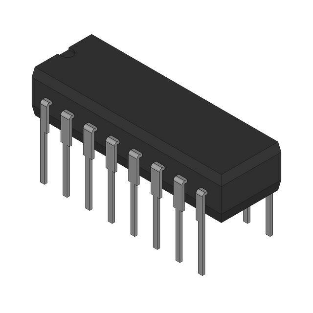
Connection Diagrams
16-Lead Ceramic Dual-In-Line Package
(NS Package Number J16A)
DS96F173
DS96F175
20164101
20164102
Top View
Top View
20-Lead Ceramic Leadless Chip Carrier (NS Package Number E20A)
20164112
20164113
Top View
*NC—No Connection
Top View
www.national.com
2
�20164111
20164110
DS96F175
DS96F173
(Each Receiver) DS96F175
Function Tables
(Each Receiver) DS96F173
Differential Inputs
A–B
VID ≥ 0.2V
VID ≤ −0.2V
Enable
E
E
Output
Y
H
X
H
X
L
H
H
X
L
X
L
L
X
L
X
Z
X
X
H
Z
Differential Inputs
A–B
Enable
E
Output
Y
VID ≥ 0.2V
H
H
VID ≤ −0.2V
H
L
X
L
Z
H = High Level
L = Low Level
Z = High Impedance (off)
X = Don't Care
3
www.national.com
DS96F173MQML/DS96F175MQML
Logic Diagrams
�DS96F173MQML/DS96F175MQML
Absolute Maximum Ratings (Note 1)
−65°C ≤ TA ≤ +175°C
300°C
Storage Temperature Range (TStg)
Lead Temperature (Soldering, 60 sec.)
Max. Package Power Dissipation at 25°C (Note 2)
Ceramic DIP (J)
Ceramic Flatpak (W)
Ceramic LCC (E)
Supply Voltage
Input Voltage, A or B Inputs
Differential Input Voltage
Enable Input Voltage
Low Level Output Current
1,500 mW
1,034 mW
1,500 mW
7.0V
±25V
±25V
7.0V
50 mA
Recommended Operating Conditions
Min
4.50
Max
5.50
Units
V
Common Mode Input Voltage (VCM)
−7
+12
V
Differential Input Voltage (VID)
−7
Supply Voltage (VCC)
+12
V
Output Current HIGH (IOH)
−400
Output Current LOW (IOL)
16
μA
mA
125
°C
Operating Temperature (TA)
−55
Quality Conformance Inspection
Mil-Std-883, Method 5005 - Group A
Subgroup
Description
1
Static tests at
Temp (°C)
+25
2
Static tests at
+125
3
Static tests at
-55
4
Dynamic tests at
+25
5
Dynamic tests at
+125
6
Dynamic tests at
-55
7
Functional tests at
+25
8A
Functional tests at
+125
8B
Functional tests at
-55
9
Switching tests at
+25
10
Switching tests at
+125
11
Switching tests at
-55
12
Settling time at
+25
13
Settling time at
+125
14
Settling time at
-55
www.national.com
4
�The following conditions apply, unless otherwise specified.
Symbol
Parameter
VCC = 5.0V, Outputs Enabled
Conditions
Notes
ICC
Supply Current
VCC = 5.5V, VID = 2V
(Note 3)
VOH
Logical "1" Output Voltage
VCC = 4.5V, IOH = -400µA,
VID = 0.2V
(Note 4)
VOL
Logical "0" Output Voltage
VCC = 4.5V, IOL = 8mA,
VID = -0.2V
(Note 4)
Max
Units
Subgroups
50
mA
1, 2, 3
V
1, 2, 3
0.45
V
1, 2, 3
0.20
V
1, 2, 3
0.20
V
1, 2, 3
0.20
V
1, 2, 3
-0.20
V
1, 2, 3
-0.20
V
1, 2, 3
-0.20
V
1, 2, 3
mA
1, 2, 3
mA
1, 2, 3
10
µA
1, 2, 3
µA
1, 2, 3
-85
-15
mA
1, 2, 3
-85
-15
mA
1, 2, 3
V
1, 2, 3
Min
2.5
VCC = 4.5V & 5.5V, VCM = 0V, VO
= 2.5V, IO = -400µA
VTH
VCC = 4.5V & 5.5V,
Differential-Input High Threshold
VCM = -12V, VO = 2.5V,
Voltage
IO = -400µA
VCC = 4.5V & 5.5V, VCM = 12V,
VO = 2.5V, IO = -400µA
VCC = 4.5V & 5.5V, VCM = 0V, VO
= 0.5V, IO = 16mA
VTL
VCC = 4.5V & 5.5V,
Differential-Input Low Threshold
VCM = -12V, VO = 0.5V,
Voltage
IO = 16mA
VCC = 4.5V & 5.5V, VCM = 12V,
VO = 0.5V, IO = 16mA
II
Input Line Current
VCC = 4.5V, VI = 12V,
Untested Inputs are 0V
VCC = 5.5V, VI = -7V,
Untested Inputs are 0V
IIH
Logical "1" Enable Input Current VCC = 5.5V, VIH = 2.7V
IIL
Logical "0" Enable Input Current VCC = 5.5V, VIL = 0.4V
IOS
Output Short Circuit Current
VIK
Enable Input Clamp Voltage
IOZ
High Impedance Output Current
1.0
VCC = 4.5V, VO = 0V
VCC = 5.5V, VO = 0V
-0.8
-100
(Note 8)
VCC = 4.5V, II = -18mA
-1.5
VCC = 5.5V, VEn = 0.8V,
VO = 0.4V,
Outputs disabled
-20
20
µA
1, 2, 3
VCC = 5.5V, VEn = 0.8V,
VO = 2.4V,
Outputs disabled
-20
20
µA
1, 2, 3
V
1, 2, 3
V
1, 2, 3
kΩ
1, 2, 3
VIH
Logical "1" Enable Input Voltage
(Note 5)
VIL
Logical "0" Enable Input Voltage
(Note 6)
RI
Input Resistance
2.0
0.8
10
5
www.national.com
DS96F173MQML/DS96F175MQML
DC Parameters
�DS96F173MQML/DS96F175MQML
AC Parameters
The following conditions apply, unless otherwise specified.
Symbol
tPHL
Parameter
Propagation Delay
Conditions
Propagation Delay
CL = 15pF
tPZH
Propagation Delay
CL = 15pF
Propagation Delay
CL = 15pF
CL = 5pF
tPHZ
Notes
CL = 15pF
tPLH
tPZL
VCC = 5.0V
(Note 7)
Propagation Delay
CL = 20pF
tPLZ
Propagation Delay
tPW
Propagation Delay
CL = 5pF
Min
Max
Units
Subgroups
22
ns
1
30
ns
2, 3
22
ns
1
30
ns
2, 3
16
ns
1
27
ns
2, 3
18
ns
1
27
ns
2, 3
20
ns
1
27
ns
2, 3
30
ns
1
37
ns
2, 3
18
ns
1
30
ns
2, 3
3.0
ns
1
8.0
ns
2
5.0
ns
3
Note 1: Absolute Maximum Ratings indicate limits beyond which damage to the device may occur. Operating Ratings indicate conditions for which the device is
functional, but do not guarantee specific performance limits. For guaranteed specifications and test conditions, see the Electrical Characteristics. The guaranteed
specifications apply only for the test conditions listed. Some performance characteristics may degrade when the device is not operated under the listed test
conditions.
Note 2: Above TA = 25°C derate J package 10 mW/°C, W package 6.90 mW/°C, E package 11.11 mW/°C.
Note 3: ICC is tested with outputs disabled (worst case), ICC enabled is guaranteed by this test.
Note 4: VOH & VOL are tested over common mode voltage range of +/−12V via the VTH / VTL tests.
Note 5: Guaranteed by VOL & VOH tests.
Note 6: Guaranteed by IOZ test.
Note 7: Testing at 20pF assures conformance to spec at 5pF.
Note 8: Only one output at a time should be shorted.
www.national.com
6
�20164104
20164103
FIGURE 1. tPLH, tPHL (Note 9, Note 10)
20164106
20164105
FIGURE 2. tHZ, tZH (Note 9, Note 10, Note 12, Note 13)
20164108
20164107
FIGURE 3. tZL, tLZ (Note 9, Note 10, Note 12, Note 13)
Note 9: The input pulse is supplied by a generator having the following characteristics: f = 1.0 MHz, 50% duty cycle, tr ≤ 6.0 ns, tf ≤ 6.0 ns, ZO = 50Ω.
Note 10: CL includes probe and stray capacitance.
Note 11: DS96F173 with active high and active low Enables are shown. DS96F175 has active high Enable only.
Note 12: All diodes are 1N916 or equivalent.
Note 13: To test the active low Enable E of DS96F173, ground E and apply an inverted input waveform to E . DS96F175 has active high enable only.
7
www.national.com
DS96F173MQML/DS96F175MQML
Parameter Measurement Information
�DS96F173MQML/DS96F175MQML
Typical Application
20164109
FIGURE 4.
Note: The line length should be terminated at both ends in its characteristic impedance. Stub lengths off the main line should be kept as short as possible
.
www.national.com
8
�Released
Revision
28–Apr-11
A
Section
Changes
New Release, Corporate format
9
2 MDS data sheets converted into one Corp. data
sheet format. MNDS96F173M-X Rev 0A0 &
MNDS96F175M-X Rev 0B0 will be archived.
www.national.com
DS96F173MQML/DS96F175MQML
Revision History
�DS96F173MQML/DS96F175MQML
Physical Dimensions inches (millimeters) unless otherwise noted
20-Lead Ceramic Leadless Chip Carrier (E)
NS Package Number E20A
16-Lead Ceramic Dual-In-Line Package (J)
NS Package Number J16A
www.national.com
10
�DS96F173MQML/DS96F175MQML
16-Lead Ceramic FlatPak (W)
NS Package Number W16A
11
www.national.com
�DS96F173MQML/DS96F175MQML EIA-485/EIA-422 Quad Differential Receivers
Notes
For more National Semiconductor product information and proven design tools, visit the following Web sites at:
www.national.com
Products
Design Support
Amplifiers
www.national.com/amplifiers
WEBENCH® Tools
www.national.com/webench
Audio
www.national.com/audio
App Notes
www.national.com/appnotes
Clock and Timing
www.national.com/timing
Reference Designs
www.national.com/refdesigns
Data Converters
www.national.com/adc
Samples
www.national.com/samples
Interface
www.national.com/interface
Eval Boards
www.national.com/evalboards
LVDS
www.national.com/lvds
Packaging
www.national.com/packaging
Power Management
www.national.com/power
Green Compliance
www.national.com/quality/green
Switching Regulators
www.national.com/switchers
Distributors
www.national.com/contacts
LDOs
www.national.com/ldo
Quality and Reliability
www.national.com/quality
LED Lighting
www.national.com/led
Feedback/Support
www.national.com/feedback
Voltage References
www.national.com/vref
Design Made Easy
www.national.com/easy
www.national.com/powerwise
Applications & Markets
www.national.com/solutions
Mil/Aero
www.national.com/milaero
PowerWise® Solutions
Serial Digital Interface (SDI) www.national.com/sdi
Temperature Sensors
www.national.com/tempsensors SolarMagic™
www.national.com/solarmagic
PLL/VCO
www.national.com/wireless
www.national.com/training
PowerWise® Design
University
THE CONTENTS OF THIS DOCUMENT ARE PROVIDED IN CONNECTION WITH NATIONAL SEMICONDUCTOR CORPORATION
(“NATIONAL”) PRODUCTS. NATIONAL MAKES NO REPRESENTATIONS OR WARRANTIES WITH RESPECT TO THE ACCURACY
OR COMPLETENESS OF THE CONTENTS OF THIS PUBLICATION AND RESERVES THE RIGHT TO MAKE CHANGES TO
SPECIFICATIONS AND PRODUCT DESCRIPTIONS AT ANY TIME WITHOUT NOTICE. NO LICENSE, WHETHER EXPRESS,
IMPLIED, ARISING BY ESTOPPEL OR OTHERWISE, TO ANY INTELLECTUAL PROPERTY RIGHTS IS GRANTED BY THIS
DOCUMENT.
TESTING AND OTHER QUALITY CONTROLS ARE USED TO THE EXTENT NATIONAL DEEMS NECESSARY TO SUPPORT
NATIONAL’S PRODUCT WARRANTY. EXCEPT WHERE MANDATED BY GOVERNMENT REQUIREMENTS, TESTING OF ALL
PARAMETERS OF EACH PRODUCT IS NOT NECESSARILY PERFORMED. NATIONAL ASSUMES NO LIABILITY FOR
APPLICATIONS ASSISTANCE OR BUYER PRODUCT DESIGN. BUYERS ARE RESPONSIBLE FOR THEIR PRODUCTS AND
APPLICATIONS USING NATIONAL COMPONENTS. PRIOR TO USING OR DISTRIBUTING ANY PRODUCTS THAT INCLUDE
NATIONAL COMPONENTS, BUYERS SHOULD PROVIDE ADEQUATE DESIGN, TESTING AND OPERATING SAFEGUARDS.
EXCEPT AS PROVIDED IN NATIONAL’S TERMS AND CONDITIONS OF SALE FOR SUCH PRODUCTS, NATIONAL ASSUMES NO
LIABILITY WHATSOEVER, AND NATIONAL DISCLAIMS ANY EXPRESS OR IMPLIED WARRANTY RELATING TO THE SALE
AND/OR USE OF NATIONAL PRODUCTS INCLUDING LIABILITY OR WARRANTIES RELATING TO FITNESS FOR A PARTICULAR
PURPOSE, MERCHANTABILITY, OR INFRINGEMENT OF ANY PATENT, COPYRIGHT OR OTHER INTELLECTUAL PROPERTY
RIGHT.
LIFE SUPPORT POLICY
NATIONAL’S PRODUCTS ARE NOT AUTHORIZED FOR USE AS CRITICAL COMPONENTS IN LIFE SUPPORT DEVICES OR
SYSTEMS WITHOUT THE EXPRESS PRIOR WRITTEN APPROVAL OF THE CHIEF EXECUTIVE OFFICER AND GENERAL
COUNSEL OF NATIONAL SEMICONDUCTOR CORPORATION. As used herein:
Life support devices or systems are devices which (a) are intended for surgical implant into the body, or (b) support or sustain life and
whose failure to perform when properly used in accordance with instructions for use provided in the labeling can be reasonably expected
to result in a significant injury to the user. A critical component is any component in a life support device or system whose failure to perform
can be reasonably expected to cause the failure of the life support device or system or to affect its safety or effectiveness.
National Semiconductor and the National Semiconductor logo are registered trademarks of National Semiconductor Corporation. All other
brand or product names may be trademarks or registered trademarks of their respective holders.
Copyright© 2011 National Semiconductor Corporation
For the most current product information visit us at www.national.com
National Semiconductor
Americas Technical
Support Center
Email: support@nsc.com
Tel: 1-800-272-9959
www.national.com
National Semiconductor Europe
Technical Support Center
Email: europe.support@nsc.com
National Semiconductor Asia
Pacific Technical Support Center
Email: ap.support@nsc.com
National Semiconductor Japan
Technical Support Center
Email: jpn.feedback@nsc.com
�