�������
SLES040 − JUNE 2002
���
���
� ��
���� ��
������
�� ��
�
�����
�
�����
����
�
�� ���������
FEATURES
D Supports DSD and PCM Formats
D Supports TDMCA
D Accepts 16-, 18-, 20- and 24-Bit Audio Data for
PCM Format
D Analog Performance (VCC = 5 V):
−
Dynamic Range: 108 dB, Typical
−
SNR: 108 dB, Typical
−
THD+N: 0.0012%, Typical
Digital Filter Rolloff: Sharp or Slow Soft
Mute
−
Three Zero Flags
D Dual Supply Operation:
−
5-V Analog, 3.3-V Digital
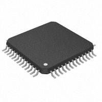
D Package: 52-Pin TQFP
Full-Scale Output: 4 Vpp, Typical
Includes 8× Oversampling Digital Filter for
PCM Format:
APPLICATIONS
D Universal A/V Players
D SACD Players
D Car Audio Systems
D Other Applications Requiring 24-Bit Audio
−
Stopband Attenuation: –60 dB
DESCRIPTION
−
Passband Ripple: ±0.02 dB
−
D
−
D Includes Digital DSD FILTER for DSD Format:
−
Passband: 50 kHz, 70 kHz, 60 kHz at –3 dB
D Sampling Frequency:
−
PCM Mode: 10 kHz to 200 kHz
−
DSD Mode: 64 × 44.1 kHz
D System Clock:
−
128 fS, 192 fS, 256 fS, 384 fS, 512 fS, 768 fS
D Data Formats:
−
Standard, I2S, and Left-Justified for PCM
Direct Stream Digital
D User-Programmable Mode Controls:
−
Digital Attenuation
−
Digital De-Emphasis
The DSD1608 is a CMOS, monolithic, 8-channel
digital-to-analog converter which supports both PCM
audio data format and direct stream digital (DSD) audio
data format. The device includes an 8× digital
interpolation filter and a digital DSD filter with three
selectable frequency-response curves, followed by
Texas Instruments’ enhanced multilevel delta-sigma
modulator, which employs 4th-order noise shaping and
8-level amplitude quantization to achieve excellent
dynamic performance and improved tolerance to clock
jitter. Sampling rates up to 192 kHz for the PCM mode
and 64 × 44.1 kHz for the DSD mode are supported. A
full set of user-programmable functions is accessible
through a 4-wire serial control port, which supports
register write and read functions. The DSD1608
supports the time-division-multiplexed command and
audio data (TDMCA) format. The DSD1608 is available
in a 52-pin TQFP package.
Please be aware that an important notice concerning availability, standard warranty, and use in critical applications of Texas Instruments
semiconductor products and disclaimers thereto appears at the end of this data sheet.
���������� �
�
�������!��� �" #$��%�! �" �� &$'(�#�!��� )�!%* ���)$#!"
#������ !� "&%#���#�!���" &%� !+% !%��" �� �%,�" ��"!�$�%�!" "!��)��) -�����!.*
���)$#!��� &��#%""��/ )�%" ��! �%#%""���(. ��#($)% !%"!��/ �� �(( &����%!%�"*
Copyright 2002, Texas Instruments Incorporated
��������
www.ti.com
SLES040 − JUNE 2002
This integrated circuit can be damaged by ESD. Texas Instruments recommends that all integrated circuits be handled with appropriate
precautions. Failure to observe proper handling and installation procedures can cause damage.
ESD damage can range from subtle performance degradation to complete device failure. Precision integrated circuits may be more susceptible to
damage because very small parametric changes could cause the device not to meet its published specifications.
ORDERING INFORMATION
PRODUCT
PACKAGE
PACKAGE
DESIGNATOR
OPERATION
TEMPERATURE
RANGE
PACKAGE
MARKING
DSD1608PAH
52-lead TQFP
PAH
−25°C to 85°C
DSD1608
ORDERING
NUMBER
TRANSPORT
MEDIA
DSD1608PAH
Tube
DSD1608PAHR
Tape and reel
ABSOLUTE MAXIMUM RATINGS
over operating free-air temperature range unless otherwise noted(1)
DSD1608
VCC1–VCC7
VDD1, VDD2
6.5 V
Supply voltage differences: VCC1–VCC7, VDD1, VDD2
Ground voltage differences: AGND1–6, DGND1, DGND2
±0.1 V
Supply voltage
4V
±0.1 V
Digital input voltage: PLRCK, PBCK, PDATA1–PDATA4, DSD1–DSD8, DBCK, DSCK, PSCK, RST
–0.3 V to 6.5 V
Digital input voltage: MC, MS, MDI, ZERO1, ZERO2, ZERO38, MDO
–0.3 V to (VDD + 0.3 V)
Analog input voltage
–0.3 V to (VCC + 0.3 V)
±10 mA
Input current (any pins except supplies)
Operating temperature
–40°C to 85°C
Storage temperature
–55°C to 150°C
Junction temperature
150°C
Lead temperature (soldering)
260°C, 5 s
Package temperature (IR reflow, peak)
235°C, 10 s
(1) Stresses beyond those listed under “absolute maximum ratings” may cause permanent damage to the device. These are stress ratings only, and
functional operation of the device at these or any other conditions beyond those indicated under “recommended operating conditions” is not
implied. Exposure to absolute-maximum-rated conditions for extended periods may affect device reliability.
ELECTRICAL CHARACTERISTICS
at TA = 25°C, VDD = 3.3 V, VCC = 5 V; in PCM mode, fS = 44.1 kHz, system clock = 256 fS, 24-bit data; in DSD mode, fS = 2.8224 MHz
(= 64 × 44.1 kHz), system clock = 256 × 44.1 kHz, 1-bit data (unless otherwise noted)
PARAMETER
TEST CONDITIONS
MIN
Resolution
TYP
MAX
24
UNIT
Bits
DATA FORMAT (PCM MODE)
Standard, I2S, left justified
Audio data interface format
Audio data bit length
16-, 18-, 20-, 24-bit selectable
Audio data format
fS
Sampling frequency
MSB first, 2s complement
fS = 44.1 kHz
10
200
kHz
128 fS, 192 fS, 256 fS, 384 fS,
512 fS, 768 fS
System clock frequency
DATA FORMAT (DSD MODE)
Audio data interface format
Direct stream digital (DSD)
Audio data bit length
fS
Sampling frequency
1 bit
fS = 44.1 kHz
fS = 44.1 kHz
64 fS
Hz
System clock frequency
256 fS, 384 fS, 512 fS, 768 fS
kHz
(1) Pins 50, 51, 34, 33, 37, 38–45, 46–49: PBCK, PLRCK, DSCK, PSCK, DBCK, DSD1–DSD8, PDATA1–PDATA4.
(2) Pins 2, 3, 4, 36: MDI, MS, MC, RST.
(3) Pins 5–8: MDO, ZERO1, ZERO2, ZERO38.
(4) Analog performance specs are measured in the averaging mode using the System Twot audio measurement system by Audio Precisiont.
(5) These specs are measured under the condition that the OVR1, OVR0 in mode registers are set to (0,1). (The oversampling rate of the modulator
is 64 fS.) If the OVR1, OVR0 are (0,0) (32 fS oversampling: default), the specs are the same as at fS = 96 kHz.
2
��������
www.ti.com
SLES040 − JUNE 2002
ELECTRICAL CHARACTERISTICS(continued)
at TA = 25°C, VDD = 3.3 V, VCC = 5 V; in PCM mode, fS = 44.1 kHz, system clock = 256 fS, 24-bit data; in DSD mode, fS = 2.8224 MHz
(= 64 × 44.1 kHz), system clock = 256 × 44.1 kHz, 1-bit data (unless otherwise noted)
PARAMETER
TEST CONDITIONS
MIN
TYP
MAX
UNIT
DIGITAL INPUT/OUTPUT
Logic family
VIH
VIL
IIH(1)
IIL(1)
IIH(2)
IIL(2)
VOH (3)
VOL (3)
TTL-compatible
2
Input logic level
Input logic current
Output logic level
0.8
VIN = VDD
VIN = 0 V
10
–10
VIN = VDD
VIN = 0 V
IOH = –2 mA
IOL = +2 mA
Vdc
65
100
µA
–10
2.4
1
Vdc
DYNAMIC PERFORMANCE(4) (PCM MODE)
fS = 44.1 kHz
fS = 96 kHz
fS = 192 kHz(5)
0.0012%
THD+N at VOUT = 0 dB
0.0012%
THD+N at VOUT = –3 dB
fS = 44.1 kHz
fS = 96 kHz
fS = 192 kHz(5)
EIAJ, A-weighted, fS = 44.1 kHz
Dynamic range
Channel separation
0.002%
0.002%
104
108
108
EIAJ, A-weighted, fS = 192 kHz(5)
107
104
108
EIAJ, A-weighted, fS = 192 kHz(5)
107
101
dB
108
EIAJ, A-weighted, fS = 96 kHz
fS = 44.1 kHz
fS = 96 kHz
fS = 192 kHz(5)
0.0018%
0.0015%
EIAJ, A-weighted, fS = 96 kHz
EIAJ, A-weighted, fS = 44.1 kHz
Signal-to-noise ratio
0.0015%
dB
104
104
dB
103
±0.5
Level linearity error
VOUT = –90 dB
DYNAMIC PERFORMANCE(4) DSD MODE (at fS = 64 × 44.1 kHz)
THD+N at VOUT = 0 dB
dB
0.0012%
Dynamic range
EIAJ, A-weighted
108
dB
Signal-to-noise ratio
EIAJ, A-weighted
108
dB
104
dB
±0.5
dB
Channel separation
Level linearity error
VOUT = −90 dB
DC ACCURACY
Gain error
±1
±6
% FSR
Gain mismatch, channel-to-channel
±1
±3
% FSR
±30
±60
mV
Bipolar zero error
V OUT = 0.5 VCC at BPZ
ANALOG OUTPUT
Output voltage
Full scale (0 dB)
80% of VCC
Center voltage
Load impedance
50% of VCC
AC load
4
Vpp
Vdc
kΩ
(1) Pins 50, 51, 34, 33, 37, 38–45, 46–49: PBCK, PLRCK, DSCK, PSCK, DBCK, DSD1–DSD8, PDATA1–PDATA4.
(2) Pins 2, 3, 4, 36: MDI, MS, MC, RST.
(3) Pins 5–8: MDO, ZERO1, ZERO2, ZERO38.
(4) Analog performance specs are measured in the averaging mode using the System Twot audio measurement system by Audio Precisiont.
(5) These specs are measured under the condition that the OVR1, OVR0 in mode registers are set to (0,1). (The oversampling rate of the modulator
is 64 fS.) If the OVR1, OVR0 are (0,0) (32 fS oversampling: default), the specs are the same as at fS = 96 kHz.
3
��������
www.ti.com
SLES040 − JUNE 2002
ELECTRICAL CHARACTERISTICS(continued)
at TA = 25°C, VDD = 3.3 V, VCC = 5 V; in PCM mode, fS = 44.1 kHz, system clock = 256 fS, 24-bit data; in DSD mode, fS = 2.8224 MHz
(= 64 × 44.1 kHz), system clock = 256 × 44.1 kHz, 1-bit data (unless otherwise noted)
PARAMETER
TEST CONDITIONS
MIN
TYP
MAX
UNIT
DIGITAL FILTER PERFORMANCE
8× INTERPOLATION FILTER (SHARP ROLL OFF FILTER)
Pass band
±0.02 dB
0.454 fS
Hz
Pass band
–3 dB
0.487 fS
Hz
Stop band
0.546 fS
Hz
±0.02
Pass-band ripple
Stop-band attenuation
Stop band = 0.546 fS
–60
Delay Time
dB
dB
23/fS
s
8× INTERPOLATION FILTER (SLOW ROLL OFF FILTER)
Pass band
–0.5 dB
0.308 fS
Hz
Pass band
–3 dB
0.432 fS
Hz
Stop band
0.832 fS
Pass-band ripple
0.308 fS
Stop-band attenuation
0.832 fS
Hz
±0.5
–58
Delay time
dB
dB
23/fS
s
±0.1
dB
DE-EMPHASIS FILTER (PCM MODE ONLY)
De-emphasis error
At fS = 32 kHz, 44.1 kHz or 48 kHz
DSD FILTER (FILTER-1)
Pass band
At –3 dB
Stop-band attenuation
At 100 kHz
50
kHz
–18
dB
DSD FILTER (FILTER-2)
Pass band
At –3 dB
Stop-band attenuation
At 100 kHz
70
kHz
–9.8
dB
60
kHz
–17
dB
DSD FILTER (FILTER-3)
Pass band
At –3 dB
Stop-band attenuation
At 100 kHz
INTERNAL ANALOG FILTER PERFORMANCE
At 20 kHz
Frequency response
–0.02
At 44 kHz
–0.1
At 50 kHz
–0.12
At 100 kHz
–0.5
dB
POWER SUPPLY REQUIREMENTS
VDD
VCC
3
3.3
3.6
4.5
5.0
5.5
fS = 44.1 kHz
fS = 192 kHz
28
40
DSD mode
45
fS = 44.1 kHz
fS = 192 kHz
36
fS = 44.1 kHz
fS = 192 kHz
270
Voltage range
IDD
Supply current
ICC
Power dissipation
Vdc
74
mA
50
38
430
380
mW
(1) Pins 50, 51, 34, 33, 37, 38–45, 46–49: PBCK, PLRCK, DSCK, PSCK, DBCK, DSD1–DSD8, PDATA1–PDATA4.
(2) Pins 2, 3, 4, 36: MDI, MS, MC, RST.
(3) Pins 5–8: MDO, ZERO1, ZERO2, ZERO38.
(4) Analog performance specs are measured in the averaging mode using the System Twot audio measurement system by Audio Precisiont.
(5) These specs are measured under the condition that the OVR1, OVR0 in mode registers are set to (0,1). (The oversampling rate of the modulator
is 64 fS.) If the OVR1, OVR0 are (0,0) (32 fS oversampling: default), the specs are the same as at fS = 96 kHz.
4
��������
www.ti.com
SLES040 − JUNE 2002
ELECTRICAL CHARACTERISTICS(continued)
at TA = 25°C, VDD = 3.3 V, VCC = 5 V; in PCM mode, fS = 44.1 kHz, system clock = 256 fS, 24-bit data; in DSD mode, fS = 2.8224 MHz
(= 64 × 44.1 kHz), system clock = 256 × 44.1 kHz, 1-bit data (unless otherwise noted)
PARAMETER
TEST CONDITIONS
MIN
TYP
MAX
UNIT
TEMPERATURE RANGE
Operating temperature
–25
85
°C
θJA
Thermal resistance
52 TQFP
70
°C/W
(1) Pins 50, 51, 34, 33, 37, 38–45, 46–49: PBCK, PLRCK, DSCK, PSCK, DBCK, DSD1–DSD8, PDATA1–PDATA4.
(2) Pins 2, 3, 4, 36: MDI, MS, MC, RST.
(3) Pins 5–8: MDO, ZERO1, ZERO2, ZERO38.
(4) Analog performance specs are measured in the averaging mode using the System Twot audio measurement system by Audio Precisiont.
(5) These specs are measured under the condition that the OVR1, OVR0 in mode registers are set to (0,1). (The oversampling rate of the modulator
is 64 fS.) If the OVR1, OVR0 are (0,0) (32 fS oversampling: default), the specs are the same as at fS = 96 kHz.
PIN ASSIGNMENTS
27
29
28
30
32
31
33
35
34
36
40
26
41
42
25
24
43
23
44
45
22
21
DSD1608
46
20
13
VCOM2
VCC7
VCC6
AGND5
VCC5
AGND4
VCC4
AGND3
VCC3
AGND2
VCC2
VCC1
VCOM1
DGND1
MDI
MS
MC
MDO
ZERO1
ZERO2
ZERO38
VOUT4
VOUT3
VOUT2
VOUT1
AGND1
11
12
14
10
52
8
9
16
15
7
17
50
51
5
6
49
4
19
18
2
3
47
48
1
DSD3
DSD4
DSD5
DSD6
DSD7
DSD8
PDATA1
PDATA2
PDATA3
PDATA4
PBCK
PLRCK
VDD1
38
37
39
DSD2
DSD1
DBCK
RST
VDD2
DSCK
PSCK
DGND2
VOUT5
VOUT6
VOUT7
VOUT8
AGND6
PAH PACKAGE
(TOP VIEW)
Audio Precision and System Two are trademarks of Audio Precision, Inc.
Other trademarks are the property of their respective owners.
5
��������
www.ti.com
SLES040 − JUNE 2002
Terminal Functions
TERMINAL
I/O
DESCRIPTION
NAME
NO.
AGND1
13
—
Analog ground
AGND2
17
—
Analog ground
AGND3
19
—
Analog ground
AGND4
21
—
Analog ground
AGND5
23
—
Analog ground
AGND6
27
—
Analog ground
DBCK
37
I
DGND1
1
—
Digital ground
DGND2
32
—
Digital ground
DSCK
34
I
System clock input (DSD). Input frequency is 256, 384, 512 or 768 fS (3)
DSD1
38
I
DSD audio data input for VOUT1 (DSD) (3)
DSD2
39
I
DSD audio data input for VOUT2 (DSD) (3)
DSD3
40
I
DSD audio data input for VOUT3 (DSD) (3)
DSD4
41
I
DSD audio data input for VOUT4 (DSD) (3)
DSD5
42
I
DSD audio data input for VOUT5 (DSD) (3)
DSD6
43
I
DSD audio data input for VOUT6 (DSD) (3)
DSD7
44
I
DSD audio data input for VOUT7 (DSD) (3)
DSD8
45
I
DSD audio data input for VOUT8 (DSD) (3)
MC
4
I
Mode control clock input (1)
MDI
2
I
Mode control data input (1)
MDO
5
O
Mode control read back data output (4)
MS
3
I
Chip select for mode control (1)
PBCK
50
I
Audio data bit clock input (PCM) (3)
PDATA1
46
I
Serial audio data input for VOUT1 and VOUT2 (PCM) (3)
PDATA2
47
I
Serial audio data input for VOUT3 and VOUT4 (PCM) (3)
PDATA3
48
I
Serial audio data input for VOUT5 and VOUT6 (PCM) (3)
PDATA4
49
I
Serial audio data input for VOUT7 and VOUT8 (PCM) (3)
PLRCK
51
I
Audio data L/R clock input (PCM) (3)
PSCK
33
I
System clock input (PCM). Input frequency is 128, 192, 256, 384, 512 or 768 fS (3)
RST
36
I
System reset, active LOW (2)
VCC1
15
—
Analog power supply, 5 V
VCC2
16
—
Analog power supply, 5 V
VCC3
18
—
Analog power supply, 5 V
VCC4
20
—
Analog power supply, 5 V
VCC5
22
—
Analog power supply, 5 V
VCC6
24
—
Analog power supply, 5 V
VCC7
25
—
Analog power supply, 5 V
DSD audio data bit clock input (DSD) (3)
VCOM1
14
O
Common voltage output 1. This pin should be bypassed with a 10-µF capacitor to AGND.
(1) Schmitt-trigger input with internal pulldown.
(2) Schmitt-trigger input with internal pulldown, 5-V tolerant.
(3) Schmitt-trigger input, 5-V tolerant.
(4) 3-state output.
6
��������
www.ti.com
SLES040 − JUNE 2002
Terminal Functions (continued)
TERMINAL
I/O
DESCRIPTION
NAME
NO.
VCOM2
26
O
Common voltage output 2. This pin should be bypassed with a 10-µF capacitor to AGND.
VDD1
52
—
Digital power supply, 3.3 V
VDD2
35
—
Digital power supply, 3.3 V
VOUT1
12
O
Voltage output for audio signal corresponding to L-channel on PDATA1 or DSD1
VOUT2
11
O
Voltage output for audio signal corresponding to R-channel on PDATA1 or DSD2
VOUT3
10
O
Voltage output for audio signal corresponding to L-channel on PDATA2 or DSD3
VOUT4
9
O
Voltage output for audio signal corresponding to R-channel on PDATA2 or DSD4
VOUT5
31
O
Voltage output for audio signal corresponding to L-channel on PDATA3 or DSD5
VOUT6
30
O
Voltage output for audio signal corresponding to R-channel on PDATA3 or DSD6
VOUT7
29
O
Voltage output for audio signal corresponding to L-channel on PDATA4 or DSD7
VOUT8
28
O
Voltage output for audio signal corresponding to R-channel on PDATA4 or DSD8
ZERO1
6
O
Zero data flag for VOUT1
ZERO2
7
O
Zero data flag for VOUT2
ZERO38
8
O
Zero data flag for VOUT3–VOUT8
(1) Schmitt-trigger input with internal pulldown.
(2) Schmitt-trigger input with internal pulldown, 5-V tolerant.
(3) Schmitt-trigger input, 5-V tolerant.
(4) 3-state output.
7
��������
www.ti.com
SLES040 − JUNE 2002
BLOCK DIAGRAM
Enhanced
Multilevel
Delta-Sigma
Modulator
System Clock
8
PCM
Filter
(x8 DF)
Function
Control
VOUT2
DAC
Output Amp and
Low-Pass Filter
DAC
Output Amp and
Low-Pass Filter
VOUT4
DAC
Output Amp and
Low-Pass Filter
VOUT5
DAC
Output Amp and
Low-Pass Filter
VOUT6
DAC
Output Amp and
Low-Pass Filter
DAC
Output Amp and
Low-Pass Filter
Power Supply
ZERO38
ZERO2
Zero Detect
ZERO1
RST
MS
MC
MDI
MDO
PCM
I/F
Output Amp and
Low-Pass Filter
DSD
Filter
PBCK
PLRCK
PDATA1
PDATA2
PDATA3
PDATA4
DAC
AGND1−6
Clock
VOUT1
VCC1−7
System
Output Amp and
Low-Pass Filter
DGND1, 2
PSCK
DSCK
DSD
I/F
DAC
VDD1, 2
DBCK
DSD1
DSD2
DSD3
DSD4
DSD5
DSD6
DSD7
DSD8
VCOM1
VOUT3
VCOM2
VOUT7
VOUT8
��������
www.ti.com
SLES040 − JUNE 2002
TYPICAL PERFORMANCE CURVES
DIGITAL FILTER—PCM MODE
8× Interpolation Filter (De-Emphasis Off)
AMPLITUDE
vs
FREQUENCY
0
0
−20
−20
−40
−40
Amplitude − dB
Amplitude − dB
AMPLITUDE
vs
FREQUENCY
−60
−60
−80
−80
−100
−100
−120
−120
0
1
2
3
4
0
1
Frequency [x fs]
2
3
4
Frequency [x fs]
Figure 1. Frequency Response (Sharp Rolloff)
Figure 2. Frequency Response (Slow Rolloff)
AMPLITUDE
vs
FREQUENCY
AMPLITUDE
vs
FREQUENCY
0.05
2
0.04
1
0.03
0
Amplitude − dB
Amplitude − dB
0.02
0.01
0.00
−0.01
−0.02
−1
−2
−3
−0.03
−4
−0.04
−0.05
0.0
0.1
0.2
0.3
0.4
Frequency [x fs]
Figure 3. Pass-Band Ripple (Sharp Rolloff)
0.5
−5
0.0
0.1
0.2
0.3
0.4
0.5
Frequency [x fs]
Figure 4. Frequency Response (Slow Rolloff)
9
��������
www.ti.com
SLES040 − JUNE 2002
De-Emphasis Curves
DE-EMPHASIS LEVEL
vs
FREQUENCY
DE-EMPHASIS ERROR
vs
FREQUENCY
0
0.5
VCC = 5 V
fs = 32 kHz
TA = 25°C
−1
0.3
De-emphasis Error − dB
De-emphasis Level − dB
−2
VCC = 5 V
fs = 32 kHz
TA = 25°C
0.4
−3
−4
−5
−6
−7
0.2
0.1
−0.0
0.0
−0.1
−0.2
−8
−0.3
−9
−0.4
−10
−0.5
0
2
4
6
8
10
12
14
0
2
4
f − Frequency − kHz
DE-EMPHASIS LEVEL
vs
FREQUENCY
10
12
14
DE-EMPHASIS ERROR
vs
FREQUENCY
0
0.5
VCC = 5 V
fs = 44.1 kHz
TA = 25°C
−1
VCC = 5 V
fs = 44.1 kHz
TA = 25°C
0.4
0.3
De-emphasis Error − dB
−2
De-emphasis Level − dB
8
Figure 6
Figure 5
−3
−4
−5
−6
−7
0.2
0.1
−0.0
0.0
−0.1
−0.2
−8
−0.3
−9
−0.4
−10
−0.5
0
2
4
6
8
10
12
14
f − Frequency − kHz
Figure 7
10
6
f − Frequency − kHz
16
18
20
0
2
4
6
8
10
12
14
f − Frequency − kHz
Figure 8
16
18
20
��������
www.ti.com
SLES040 − JUNE 2002
De-Emphasis Curves (Continued)
DE-EMPHASIS LEVEL
vs
FREQUENCY
DE-EMPHASIS ERROR
vs
FREQUENCY
0
0.5
VCC = 5 V
fs = 48 kHz
TA = 25°C
−1
0.3
De-emphasis Error − dB
De-emphasis Level − dB
−2
VCC = 5 V
fs = 48 kHz
TA = 25°C
0.4
−3
−4
−5
−6
−7
0.2
0.1
−0.0
0.0
−0.1
−0.2
−8
−0.3
−9
−0.4
−10
−0.5
0
2
4
6
8
10
12
14
f − Frequency − kHz
Figure 9
16
18
20
22
0
2
4
6
8
10
12
14
16
18
20
22
f − Frequency − kHz
Figure 10
11
��������
www.ti.com
SLES040 − JUNE 2002
ANALOG DYNAMIC PERFORMANCE
DYNAMIC RANGE
vs
SUPPLY VOLTAGE
TOTAL HARMONIC DISTORTION + NOISE (−3 dB)
vs
SUPPLY VOLTAGE
110
0.0016
VCC = 5 V
fs = 44.1 kHz
TA = 25°C
109
VCC = 5 V
fs = 44.1 kHz
TA = 25°C
0.0014
Dynamic Range − dB
THD+N − Total Harmonic Distortion + Noise (−3 dB) − %
Supply Voltage Characteristics
192 kHz
0.0012
96 kHz
0.0010
44.1 kHz
0.0008
4.0
4.5
96 kHz
108
192 kHz
107
44.1 kHz
106
5.0
5.5
105
4.0
6.0
4.5
Figure 11
106
105
Channel Separation − dB
SNR − dB
VCC = 5 V
fs = 44.1 kHz
TA = 25°C
108
96 kHz
192 kHz
107
44.1 kHz
VCC = 5 V
fs = 44.1 kHz
TA = 25°C
44.1 kHz
104
96 kHz
103
192 kHz
102
106
4.5
5.0
5.5
VCC − Supply Voltage − V
Figure 13
6.0
101
4.0
4.5
5.0
5.5
VCC − Supply Voltage − V
Figure 14
All specifications at TA = +25°C, VCC = 5.0 V, VDD = 3.3 V, fS = 44.1 kHz, system clock = 384 fS and 24-bit data, unless otherwise noted
12
6.0
CHANNEL SEPARATION
vs
SUPPLY VOLTAGE
110
105
4.0
5.5
Figure 12
SNR
vs
SUPPLY VOLTAGE
109
5.0
VCC − Supply Voltage − V
VCC − Supply Voltage − V
6.0
��������
www.ti.com
SLES040 − JUNE 2002
Temperature Characteristics
DYNAMIC RANGE
vs
FREE-AIR TEMPERATURE
110
0.18
0.0018
VCC = 5 V
fs = 44.1 kHz
VCC = 5 V
fs = 44.1 kHz
0.16
0.0016
109
Dynamic Range − dB
THD+N − Total Harmonic Distortion + Noise (−3 dB) − %
TOTAL HARMONIC DISTORTION + NOISE (−3 dB)
vs
FREE-AIR TEMPERATURE
0.14
0.0014
192 kHz
0.12
0.0012
96 kHz
0.10
0.0010
44.1 kHz
44.1 kHz
96 kHz
108
192 kHz
107
0.08
0.0008
0.06
0.0006
−50
−25
0
25
50
75
106
−50
100
TA − Free-Air Temperature − °C
−25
0
25
50
75
100
75
100
TA − Free-Air Temperature − °C
Figure 16
Figure 15
SNR
vs
FREE-AIR TEMPERATURE
CHANNEL SEPARATION
vs
FREE-AIR TEMPERATURE
106
110
VCC = 5 V
fs = 44.1 kHz
VCC = 5 V
fs = 44.1 kHz
105
Channel Separation − dB
109
SNR − dB
44.1 kHz
108
96 kHz
192 kHz
107
44.1 kHz
104
96 kHz
103
192 kHz
102
106
−50
−25
0
25
50
TA − Free-Air Temperature − °C
Figure 17
75
100
101
−50
−25
0
25
50
TA − Free-Air Temperature − °C
Figure 18
All specifications at TA = +25°C, VCC = 5.0 V, VDD = 3.3 V, fS = 44.1 kHz, system clock = 384 fS and 24-bit data, unless otherwise noted
13
��������
www.ti.com
SLES040 − JUNE 2002
DIGITAL FILTER—DSD MODE
AMPLITUDE
vs
FREQUENCY
5
Filter 3
0
Filter 1
Amplitude − dB
−5
Filter 2
−10
−15
−20
−25
−30
−35
1
10
100
1k
f − Frequency − kHz
Figure 19
SYSTEM CLOCK AND RESET FUNCTIONS
System clock input
The DSD1608 requires a system clock for operating the digital interpolation filter, digital DSD filter and multilevel
delta-sigma modulator. The system clock is applied to PSCK (pin 33) in the PCM mode and to DSCK (pin 34) in the
DSD mode. When CKCE (control register 10, B3) is not set to 1, the system clock is applied to PSCK in the DSD
mode. The DSD1608 has a system clock detection circuit. Table 1 shows examples of system clock frequencies for
common audio sampling rates.
Figure 20 shows the timing requirements for the system clock input. For optimal performance, it is important to use
a clock source with low phase jitter and noise. Texas Instruments’ PLL1700 multiclock generator is an excellent
choice for providing the DSD1608 system.
In the PCM mode, the oversampling rate of digital filter is 4× when a 128-fS or 192-fS system clock is applied to the
DSD1608. When a 256-fS, 384-fS, 512-fS, or 768-fS system clock is applied, the oversampling rate is 8×.
Table 1. System Clock Rates for Common Audio Sampling Frequencies
MODE
SYSTEM CLOCK FREQUENCY (fSCLK) (MHz)
SAMPLING
FREQUENCY
128 fS
192 fS
256 fS
16kHz
2.0480
3.0720
4.0960
32kHz
4.0960
6.1440
8.1920
44.1kHz
5.6488
8.4672
11.2896
384 fS
512 fS
768 fS
6.1440
8.1920
12.2880
12.2880
16.3840
24.5760
16.9344
22.5792
33.8688
48kHz
6.1440
9.2160
12.2880
18.4320
24.5760
36.8640
88.2kHz
11.2896
16.9344
22.5792
33.8688
45.1584
67.7376
96kHz
12.2880
18.4320
24.5760
36.8640
49.1520
73.7280
192kHz
24.5760
36.8640
See Note
See Note
See Note
See Note
DSD
64×44.1kHz
—
—
11.2896
NOTE: This system clock is not supported for the given sampling frequency.
16.9344
22.5792
33.8688
PCM
14
��������
www.ti.com
SLES040 − JUNE 2002
t(SCKH)
System Clock
(PSCK, DSCK)
H
2V
L
0.8 V
t(SCY)
t(SCKL)
SYMBOL
t(SCY)
t(SCKH)
t(SCKL)
PARAMETERS
System clock pulse cycle time
MIN
MAX
UNIT
13
ns
System clock pulse duration high
0.4 tSCY
ns
System clock pulse duration low
0.4 tSCY
ns
Figure 20. System Clock Input Timing
Power-On and External Reset Functions
The DSD1608 includes a power-on reset function. Figure 21 shows the operation of this function. With VDD > 2 V,
the power-on reset function is enabled. The initialization sequence requires 1024 system clocks from the time VDD
> 2 V. After the initialization period, the DSD1608 is set to its reset default state, as described in the mode control
register section of this data sheet. The DSD1608 also includes an external reset capability using the RST input (pin
36). This allows an external controller or master reset circuit to force the DSD1608 to initialize to its reset state.
Figure 22 shows the external reset operation and timing. The RST pin is set to logic 0 for a minimum of 20 ns. When
the RST pin is set to a logic 0 state, the DSD1608 is initialized. The RST pin is then set to a logic 1 state, thus starting
the initialization sequence, which requires 1024 system clock periods.
VDD
2.4 V
2V
1.6 V
Reset
Reset Removal
Internal Reset
1024 System Clocks
System Clock
(PSCK)
Figure 21. Power-On Reset Timing
RST (Pin 36)
50% of VDD
t(RST)
Reset
Reset Removal
Internal Reset
1024 System Clocks
System Clock
SYMBOL
t(RST)
PARAMETERS
Reset pulse duration low
MIN
20
MAX
UNIT
ns
Figure 22. External Reset Timing
15
��������
www.ti.com
SLES040 − JUNE 2002
Audio Serial Interface
The DSD1608 has two audio serial interface ports: PCM audio interface port and DSD audio interface port.
In the PCM mode, the audio interface is a 3-wire serial port. It includes PLRCK (pin 51), PBCK (pin 50), and
PDATA1–PDATA4 (pins 46–49). PBCK is the serial audio bit clock, and it is used to clock the serial data present on
PDATA1–4 into the audio interface serial shift register. Serial data is clocked into the DSD1608 on the rising edge
of PBCK. PLRCK is the serial audio left/right word clock. It is used to latch serial data into the serial audio interface
internal registers.
The DSD1608 requires the synchronization of PLRCK to the system clock, but does not require a specific phase
relation between PLRCK and system clock.
If the relationship between PLRCK and system clock changes more than ±6 PBCK, internal operation is initialized
within 1/fS and analog outputs are forced to 0.5 VCC until re-synchronization between PLRCK and the system clock
is completed.
In the DSD mode, the audio interface is a 2-wire serial port. DBCK (pin 37) is the serial audio bit clock, and it is used
to clock the individual direct stream digital (DSD) audio data on DSD1–DSD8 (pins 38–45). DSD data is clocked into
the DSD1608 on the rising edge of DBCK. DBCK must be synchronous with the system clock, but does not require
a specific phase relation to the system clock. DBCK is operated at the sampling frequency fS; the fS of DSD is
64 × 44.1 kHz, nominal.
Audio Data Formats and Timing
In the PCM mode, the DSD1608 supports industry-standard audio data formats, including standard, I2S, and
left-justified. The data formats are shown in Figure 23. Data formats are selected using the format bits, FMT[2:0],
in control register 10. The default data format is 24-bit standard format. All formats require binary 2s complement,
MSB-first audio data. Figure 24 shows a detailed timing diagram for the serial audio interface.
In the DSD mode, the DSD1608 supports a DSD audio data format. The data formats are shown in Figure 25.
Figure 26 shows a detailed timing diagram for the DSD audio data interface.
Serial Control Interface
The serial control interface is a 4-wire serial port which operates completely asynchronously from the serial audio
interface and the system clock. The serial control interface is used to access the on-chip mode registers. The control
interface includes MDI (pin 2), MDO (pin 5), MC (pin 4), and MS (pin 3). MDI is the serial data input, used to program
the mode registers. MDO is the serial data output, used to read back the values of the mode registers. MC is the serial
bit clock, used to shift data into the control port, and MS is the chip select for the control port.
16
��������
www.ti.com
SLES040 − JUNE 2002
(1) STD Format: L-Channel = H, R-Channel = L
1/fS
PLRCK
R-Channel
L-Channel
PBCK
(a) Data Word = 16 Bit
PDATA1−4
14 15 16
1
2
15 16
MSB
1
2
15 16
LSB
(b) Data Word = 18 Bit
PDATA1−4
16 17 18
1
2
17 18
1
2
17 18
1
2
19 20
LSB
MSB
(c) Data Word = 20 Bit
PDATA1−4
18 19 20
1
2
19 20
LSB
MSB
(d) Data Word = 24 Bit
PDATA1−4
22 23 24
1
2
23 24
1
2
23 24
LSB
MSB
(2) IIS Format: L-Channel = L, R-Channel = H
1/fS
PLRCK
R-Channel
L-Channel
PBCK
Data Word = 24 Bit
1
PDATA1−4
2
23 24
MSB
1
2
23 24
1
LSB
(3) Left Justified Format: L-Channel = H, R-Channel = L
1/fS
PLRCK
R-Channel
L-Channel
PBCK
Data Word = 24 Bit
PDATA1−4
1
2
MSB
23 24
1
2
23 24
1
2
LSB
Figure 23. PCM Data Format
17
��������
www.ti.com
SLES040 − JUNE 2002
50% of VDD
PLRCK
t(BCH)
t(BCL)
t(LB)
50% of VDD
PBCK
t(BCY)
t(BL)
50% of VDD
PDATA1−4
tsu(D)
SYMBOL
th(D)
PARAMETERS
MIN
UNIT
PBCK pulse cycle time
70
ns
PBCK high-level time
30
ns
t(BCL)
t(BL)
PBCK low-level time
30
ns
PBCK rising edge to PLRCK edge
10
ns
t(LB)
tsu(D)
th(D)
PLRCK edge to PBCK rising edge
10
ns
PDATA1−4 setup time
10
ns
PDATA1−4 hold time
10
ns
Figure 24. Timing for PCM Audio Interface
t = 1/(64 x 44.1 kHz)
DBCK
DSD1−8
D0
D1
D2
D3
Figure 25. Normal Data Output Form From DSD Decoder
18
MAX
t(BCY)
t(BCH)
D4
��������
www.ti.com
SLES040 − JUNE 2002
t(BCH)
t(BCL)
50% of VDD
DBCK
t(BCY)
50% of VDD
DSD1−8
tsu(D)
th(D)
SYMBOL
PARAMETERS
MIN
350(1)
MAX
UNIT
t(BCY)
t(BCH)
DBCK pulse cycle time
DBCK high-level time
30
ns
t(BCL)
tsu(D)
DBCK low-level time
30
ns
DSD1−8 setup time
10
ns
DSD1−8 hold time
10
ns
th(D)
ns
(1) 2.8224 MHz = 64 × 44.1 kHz; this value is specified as a sampling rate of DSD.
Figure 26. Timing for DSD Audio Interface
Register Read/Write Operation
All read/write operations for the serial control port use 16-bit data words. Figure 27 shows the control data word
format. The most significant bit is the read/write (R/W) bit. For write operations, the R/W bit must be set to 0. For
read operations, the R/W bit must be set to 1. There are seven bits, labeled IDX[6:0], that set the register index (or
address) for the read or write operations. The least significant eight bits, D[7:0], contain the data to be written to the
register specified by IDX[6:0] or to be read from the register specified by IDX[6:0].
Figure 28 shows the functional timing diagram for writing or reading the serial control port. MS is held at a logic 1
state until a register needs to be written or read. To start the register write or read cycle, MS is set to logic 0. Sixteen
clocks are then provided on MC, corresponding to the 16 bits of the control data word on MDI and read back data
on MDO. After the eighth clock cycle has completed, the data from indexed mode control register appears on MDO
in read operation. After the sixteenth clock cycle has completed, the data is latched into the indexed mode control
register in write operations. To write or read subsequent data, MS must be set to 1 once.
LSB
MSB
R/W
IDX6
IDX5
IDX4
IDX3
IDX2
IDX1
IDX0
D7
D6
D5
Register Index (or Address)
D4
D3
D2
D1
D0
Register Data
Figure 27. Control Data Word Format for MDI
MS
MC
MDI
MDO
X
R/W IDX6 IDX5 IDX4 IDX3 IDX2 IDX1 IDX0 D7
High Impedance
D7
D6
D5
D4
D3
D2
D1
D0
D6
D5
D4
D3
D2
D1
D0
X
X
R/W IDX6
High Impedance
When Read Mode is Instructed
Figure 28. Serial Control Format
19
��������
www.ti.com
SLES040 − JUNE 2002
Control Interface Timing Requirements
Figure 29 shows a detailed timing diagram for the serial control interface. These timing parameters are critical for
proper control port operation.
t(MHH)
MS
50% of VDD
t(MSS)
t(MCL)
t(MCH)
th(MS)
MC
50% of VDD
t(MCY)
LSB
MDI
t(MOS)
tsu(MD)
50% of VDD
th(MD)
MDO
50% of VDD
SYMBOL
PARAMETERS
MIN
MAX
UNIT
t(MCY)
t(MCL)
MC pulse cycle time
100
ns
MC low level time
40
ns
t(MCH)
t(MHH)
MC high level time
40
ns
MS high level time
80
ns
t(MSS)
th(MS)
MS falling edge to MC rise edge
MS hold time (1)
15
ns
15
ns
th(MD)
tsu(MD)
MDI hold time
15
ns
MDI setup time
15
t(MOS)
MC falling edge to MDO stable
ns
30
ns
(1) MC rising edge for LSB-to-MS rising edge.
Figure 29. Control Interface Timing
MODE CONTROL REGISTERS
User-Programmable Mode Controls
The DSD1608 includes a number of user programmable functions which are accessed via control registers. The
registers are programmed using the serial control interface which was previously discussed in this data sheet. Table 2
lists the available mode control functions, along with their reset default conditions and associated register index.
Register Map
The mode control register map is shown in Table 3. Each register includes an index (or address) indicated by the
IDX[6:0] bits B[14:8].
20
��������
www.ti.com
SLES040 − JUNE 2002
Table 2. User-Programmable Mode Controls
FUNCTION
RESET DEFAULT
REGISTER
BIT(S)
PCM
DSD
AT1[7:0] to AT8[7:0]
√
√
8
MUT[8:1]
√
√
DAC1 to DAC8 enabled
9
DAC[8:1]
√
√
24-bit standard format
10
FMT[2:0]
√
Clock select control
Disabled
10
CKCE
Attenuation rate select
8/fS
Sharp rolloff
10
ATS
√
Rolloff control for 8× digital filter
10
FLT
√
De-emphasis function control
De-emphasis disabled
11
DM12, -34, -56, -78
√
De-emphasis sample rate control
44.1kHz
11
DMF[1:0]
√
Over sampling rate control (64 fS or 128 fS)
64 fS oversampling
11
OVR[1:0]
√
Output phase select
Normal phase
12
DRV12, -34, -56, -78
√
Zero flag polarity select
High
12
ZREV
√
Zero flag output pin select
CH1/2 flags separately
selectable
12
AZRO
√
DSD mode control
PCM mode
12
DSD
System reset
Not operated
12
SRST
DSD filter select
Filter 1
Zero flag status (read-only)
—
16
ZERO[8:1]
√
Device ID (at TDMCA)
—
17
ID[4:0]
√
Digital attenuation control, 0 dB to –∞ in 0.5 dB steps
0dB, no attenuation
Soft mute control
Mute disabled
DAC operation control
Audio data format control
0–7
13, 14
√
√
√
√
√
√
√
FS1[1:0] to FS8[1:0]
√
Table 3. Mode Control Register Map
B15
B14
B13
B12
B11
B10
B9
B8
B7
B6
B5
B4
B3
B2
B1
B0
Register 0
R/W
0
0
0
0
0
0
0
AT17
AT16
AT15
AT14
AT13
AT12
AT11
AT10
Register 1
R/W
0
0
0
0
0
0
1
AT27
AT26
AT25
AT24
AT23
AT22
AT21
AT20
Register 2
R/W
0
0
0
0
0
1
0
AT37
AT36
AT35
AT34
AT33
AT32
AT31
AT30
Register 3
R/W
0
0
0
0
0
1
1
AT47
AT46
AT45
AT44
AT43
AT42
AT41
AT40
Register 4
R/W
0
0
0
0
1
0
0
AT57
AT56
AT55
AT54
AT53
AT52
AT51
AT50
Register 5
R/W
0
0
0
0
1
0
1
AT67
AT66
AT65
AT64
AT63
AT62
AT61
AT60
Register 6
R/W
0
0
0
0
1
1
0
AT77
AT76
AT75
AT74
AT73
AT72
AT71
AT70
Register 7
R/W
0
0
0
0
1
1
1
AT87
AT86
AT85
AT84
AT83
AT82
AT81
AT80
Register 8
R/W
0
0
0
1
0
0
0
MUT8
MUT7
MUT6
MUT5
MUT4
MUT3
MUT2
MUT1
Register 9
R/W
0
0
0
1
0
0
1
DAC8
DAC7
DAC6
DAC5
DAC4
DAC3
DAC2
DAC1
Register 10
R/W
0
0
0
1
0
1
0
RSV
FLT
ATS
RSV
CKCE
FMT2
FMT1
FMT0
Register 11
R/W
0
0
0
1
0
1
1
OVR1
OVR0
DMF1
DMF0
DM78
DM56
DM34
DM12
Register 12
R/W
0
0
0
1
1
0
0
SRST
DSD
AZRO
ZREV
DRV78
DRV56
DRV34
DRV12
Register 13
R/W
0
0
0
1
1
0
1
FS41
FS40
FS31
FS30
FS21
FS20
FS11
FS10
Register 14
R/W
0
0
0
1
1
1
0
FS81
FS80
FS71
FS70
FS61
FS60
FS51
FS50
Register 16
R
0
0
1
0
0
0
0
ZERO8
ZERO7
ZERO6
ZERO5
ZERO4
ZERO3
ZERO2
ZERO1
Register 17
R
0
0
1
0
0
0
1
RSV
RSV
RSV
ID4
ID3
ID2
ID1
ID0
21
��������
www.ti.com
SLES040 − JUNE 2002
Register Definitions
Register 0
B15
B14
B13
B12
B11
B10
B9
B8
B7
B6
B5
B4
B3
B2
B1
B0
R/W
0
0
0
0
0
0
0
AT17
AT16
AT15
AT14
AT13
AT12
AT11
AT10
R/W
0
0
0
0
1
1
1
AT87
AT86
AT85
AT84
AT83
AT82
AT81
AT80
:
Register 7
R/W
Read/Write Mode Select
When R/W = 0, a write operation is performed. When R/W = 1, a read operation is performed.
ATxy
Digital Attenuation Level Setting
:PCM/DSD Mode
Where x = register number + 1 and y = 1 to 8, corresponding to the DAC output VOUT1 to VOUT8. In PCM mode, the
default value, 1111 1111b, represents 0 dB. Each DAC channel (VOUT1 to VOUT8) includes a digital attenuation
function. The attenuation level can be set from 0 dB to –119.5 dB in 0.5 dB steps or to –∞ in PCM mode, and from
6 dB to –113.5 dB or to –∞ in DSD mode. Alternatively, the attenuation level can be set to infinite attenuation (or mute).
The following table shows attenuation levels for various settings.
ATxy
DECIMAL VALUE
ATTENUATION LEVEL SETTING
PCM Mode
DSD Mode
1111 1111b
255
0 dB, no attenuation (default)
6 dB
1111 1110b
254
–0.5 dB
5.5 dB
1111 1101b
253
–1 dB
5 dB
:
:
:
:
1111 0011b
243
–6 dB
0 dB
1111 0010b
242
–6.5 dB
–0.5 dB
:
:
:
:
1000 0011b
131
–62 dB
–56 dB
1000 0010b
130
–62.5 dB
–56.5 dB
1000 0001b
129
–63 dB
–57 dB
1000 0000b
128
–63.5 dB
–57.5 dB
:
:
:
:
0111 0101b
117
–69 dB
–63 dB
:
:
:
:
0001 0000b
16
–119.5 dB
–113.5 dB
0000 1111b
15
–∞
–∞
:
:
:
:
0000 0000b
0
–∞
–∞
Register 8
R/W
B15
B14
B13
B12
B11
B10
B9
B8
B7
B6
B5
B4
B3
B2
B1
B0
R/W
0
0
0
1
0
0
0
MUT8
MUT7
MUT6
MUT5
MUT4
MUT3
MUT2
MUT1
Read/Write Mode Select
When R/W = 0, a write operation is performed. When R/W = 1, a read operation is performed.
MUTx
Soft Mute Control
:PCM/DSD Mode
Where x = 1 to 8, corresponding to the DAC output VOUT1 to VOUT8. Default value: 0
MUTx = 0
Mute disabled (default)
MUTx = 1
Mute enabled
The mute bits, MUT1 to MUT8, are used to enable or disable the soft mute function for the corresponding DAC
outputs, VOUT1 to VOUT8. The soft mute function is incorporated into the digital attenuators. When mute is disabled
(MUTx = 0), the attenuator and DAC operate normally. When mute is enabled by setting MUTx = 1, the digital
attenuator for the corresponding output is decreased from the current setting to infinite attenuation, one attenuator
step (0.5 dB) at a time. This provides pop-free muting of the DAC output. By setting MUTx = 0, the attenuator is
incremented one step at a time to the previously programmed attenuation level.
22
��������
www.ti.com
SLES040 − JUNE 2002
Register 9
B15
B14
B13
B12
B11
B10
B9
B8
B7
B6
B5
B4
B3
B2
B1
B0
R/W
0
0
0
1
0
0
1
DAC8
DAC7
DAC6
DAC5
DAC4
DAC3
DAC2
DAC1
R/W
Read/Write Mode Select
When R/W = 0, a write operation is performed. When R/W = 1, a read operation is performed.
DACx
DAC Operation Control
:PCM/DSD Mode
Where x = 1 to 8, corresponding to the DAC output VOUT1 to VOUT8. Default value: 0
DACx = 0
DAC operation enabled (default)
DACx = 1
DAC operation disabled
The DAC operation controls are used to enable and disable the DAC outputs, VOUT1 to VOUT8. When DACx = 0,
the corresponding output generates the audio waveform dictated by the data present on the DATA pin. When DACx
= 1, the corresponding output is set to the bipolar zero level, or VCC / 2. In the TDMCA mode, the DACx bits are
affected after the next PLRCK when the write operation occurs.
Register 10
B15
B14
B13
B12
B11
B10
B9
B8
B7
B6
B5
B4
B3
B2
B1
B0
R/W
0
0
0
1
0
1
0
RSV
FLT
ATS
RSV
CKCE
FMT2
FMT1
FMT0
R/W
Read/Write Mode Select
When R/W = 0, a write operation is performed. When R/W = 1, a read operation is performed.
RSV
Reserved Bit
The RSV bit must be set to 0.
FLT
Digital Filter Roll-Off Control
:PCM Mode
Default value: 0
FLT = 0
Sharp rolloff (default)
FLT = 1
Slow rolloff
The FLT bit allows the user to select the digital filter rolloff that is best suited to a particular application. Two filter rolloff
selections are available: sharp and slow. The filter responses for these selections are shown in the Typical
Performance Curves section of this data sheet.
ATS
Attenuation Rate Select
:PCM/DSD Mode
Default value: 0
ATS = 0
8/fS (default)
ATS = 1
16/fS
The ATS bit is used to select the rate at which the attenuator is decremented / incremented during level transitions.
CKCE
Clock Select Control
:DSD Mode
Default value: 0
CKCE = 0
System clock is applied to PSCK in the DSD mode (default).
CKCE = 1
System clock is applied to DSCK in the DSD mode.
The CKCE bit selects the system clock source in the DSD mode (PSCK or DSCK). The CKCE bit must be set before
the DSD bit in register 12 can be set to 1.
FMT[2:0]
Audio Interface Data Format
:PCM Mode
Default value: 000. The FMT[2:0] bits are used to select the data format for the serial audio interface. The table below
shows the available format options.
23
��������
www.ti.com
SLES040 − JUNE 2002
FMT[2:0]
Audio Data Format Select
000
24-bit standard format, right-justified data (default)
001
20-bit standard format, right-justified data
010
18-bit standard format, right-justified data
011
16-bit standard format, right-justified data
100
I2S format, 24 bits
101
Left-justified format, 24 bits
110
Reserved
111
Reserved
Register 11
B15
B14
B13
B12
B11
B10
B9
B8
B7
B6
B5
B4
B3
B2
B1
B0
R/W
0
0
0
1
0
1
1
OVR1
OVR0
DMF1
DMF0
DM78
DM56
DM34
DM12
R/W
Read/Write Mode Select
When R/W = 0, a write operation is performed. When R/W = 1, a read operation is performed.
OVR[1:0]
Delta-Sigma Oversampling Rate Select
Default value: 0
OVR[1:0]
Oversampling Rate Select
00
64× fS (default)
01
128× fS
1x
32× fS
The OVR[1:0] bits are used to change the oversampling rate of delta-sigma modulation. This function makes it easy
to design a post-low-pass filter for any sampling rate.
DMF[1:0]
De-Emphasis Sampling Frequency Select
Default value: 0
DMF[1:0]
De-Emphasis Sampling Frequency Select
00
44.1 kHz (default)
01
48 kHz
10
32 kHz
11
Reserved
The DMF[1:0] bits are used to select the sampling frequency for the digital de-emphasis function when de-emphasis
is enabled.
DMxx
De-Emphasis Function Control
Default value: 0
DMxx = 0
De-emphasis function disabled (default)
DMxx = 1
De-emphasis function enabled
The DMxx bits are used to enable or disable the digital de-emphasis function of selected channel pairs. Suffix 12,
34, 56, 78 means Channel 1 and 2, 3 and 4, 5 and 6, and 7 and 8 respectively. See the plots shown in the Typical
Performance Curves section of this data sheet.
Register 12
24
B15
B14
B13
B12
B11
B10
B9
B8
B7
B6
B5
B4
B3
B2
B1
B0
R/W
0
0
0
1
1
0
0
SRST
DSD
AZRO
ZREV
DRV78
DRV56
DRV34
DRV12
��������
www.ti.com
SLES040 − JUNE 2002
R/W
Read/Write Mode Select
When R/W = 0, a write operation is performed. When R/W = 1, a read operation is performed.
SRST
System Reset
:PCM/DSD Mode
Default value: 0. This bit is available only in the write mode.
DAC system is reset once.
SRST = 1
The SRST bit allows the user to reset DAC system. This function is same as the power-on reset. When the SRST
is set to 1, one reset pulse is generated internally. It is not necessary to set SRST to 0.
DSD
DSD Mode Control
:PCM/DSD Mode
Default value: 0
DSD = 0
PCM mode (default)
DSD = 1
DSD mode
The DSD bit allows the user to select the operation mode, PCM mode or DSD mode.
AZRO
Zero Flag Output Pin Select
:PCM Mode
Default value: 0
AZRO = 0
When ZREV = 0 and either the channel 1 or channel 2 data is continuously zero, the
ZERO1 and ZERO2 pins go HIGH. When ZREV = 1 and either the channel 1 or
channel 2 data is continuously zero, the ZERO1 and ZERO2 pins go LOW (default).
AZRO = 1
When ZREV = 0 and both the channel 1 and channel 2 data is continuously zero, the
ZERO1 and ZERO2 pins go HIGH. ZERO2 pin stay in LOW. When ZREV = 1 and both
the channel 1 and channel 2 data is continuously zero, the ZERO1 and ZERO2 pins go
LOW.
The AZRO bit allows the user to select the output form of ZERO1 and ZERO2.
ZREV
Zero Flag Polarity Select
:PCM Mode
Default value: 0
ZREV = 0
Zero flag pins HIGH at a zero detect (default)
ZREV = 1
Zero flag pins LOW at a zero detect
The ZREV bit allows the user to select the polarity of zero flag pins.
DRVxx
Output Phase Select
:PCM/DSD Mode
Default value: 0
DRVxx = 0
Normal output (default)
DRVxx = 1
Inverted output
The DRVxx bits control output analog signal phase for channel pairs. The xx suffix in the register name designates
the channel pair: -12 indicates channels 1 and 2; -34 indicates channels 3 and 4; -56 indicates channels 5 and 6; and
-78 indicates channels 7 and 8.
B15
B14
B13
B12
B11
B10
B9
B8
B7
B6
B5
B4
B3
B2
B1
B0
Register 13
R/W
0
0
0
1
1
0
1
FS41
FS40
FS31
FS30
FS21
FS20
FS11
FS10
Register 14
R/W
0
0
0
1
1
1
0
FS81
FS80
FS71
FS70
FS61
FS60
FS51
FS50
25
��������
www.ti.com
SLES040 − JUNE 2002
R/W
Read/Write Mode Select
When R/W = 0, a write operation is performed. When R/W = 1, a read operation is performed.
FSxy
DSD Filter Select
:DSD Mode
Default value: 00
FSxy
DSD Filter Select
00
Filter 1 (default)
01
Filter 2
10
Filter 3
11
Reserved
The FSxy bits allow selection of the DSD filter from three kind of filters for each channel. The x suffix in the register
name designates the channel, from 1 to 8, for which the filter is being selected. The y suffix in the register name
designates the high or low bit of the filter selection value.
B15
B14
B13
B12
B11
B10
B9
B8
B7
B6
B5
B4
B3
B2
B1
B0
R
0
0
1
0
0
0
0
ZERO8
ZERO7
ZERO6
ZERO5
ZERO4
ZERO3
ZERO2
ZERO1
Register 16
R
Read Only
ZEROx
Zero Flag
ZEROx = 0
Not zero detected on indexed channel
ZEROx = 1
Zero detected on indexed channel
The ZEROx bits indicate indexed the result of ZERO detection circuit of each channels.
Register 17
B15
B14
B13
B12
B11
B10
B9
B8
B7
B6
B5
B4
B3
B2
B1
B0
R
0
0
1
0
0
0
1
RSV
RSV
RSV
ID4
ID3
ID2
ID1
ID0
R
Read Only
RSV
Reserve Bit
The RSV bit is read as 0.
ID[4:0]
Device ID
The ID[4:0] bits show a device ID in TDMCA mode.
ANALOG OUTPUTS
The DSD1608 includes eight independent output channels: VOUT1 to VOUT8. These are unbalanced outputs, each
capable of driving 4 Vp-p typical into a 10-kΩ ac-coupled load. The internal output amplifiers for VOUT1 to VOUT8 are
biased to the dc common-mode (or bipolar zero) voltage, equal to VCC/2.
The output amplifiers include an RC continuous-time filter, which helps to reduce the out-of-band noise energy
present at the DAC outputs due to the noise shaping characteristics of the DSD1608 delta-sigma D/A converters.
The frequency response of this filter is shown in Figure 30. By itself, this filter is not enough to attenuate the
out-of-band noise to an acceptable level for many applications. An external low-pass filter is required to provide
sufficient out-of-band noise rejection. Further discussion of DAC post-filter circuits is provided in the Applications
Information section of this data sheet.
26
��������
www.ti.com
SLES040 − JUNE 2002
RESPONSE
vs
FREQUENCY
10
0
Response − dB
−10
−20
−30
−40
−50
−60
100
1k
10k
100k
1M
10M
f − Frequency − Hz
Figure 30. Analog Output Filter Performance (100 Hz−10 MHz)
ZERO FLAGS
The DSD1608 includes circuitry for detecting an all-zero data condition for the audio data input pin and output pins
for indicating the result.
Zero Detect Condition
Zero detection for each channel or combination of channels is independent from any other.
In PCM mode, if the data for a given channel or channel combination remains at a 0 level for 1024 sample periods
(or PLRCK clock periods), a zero-detect condition exists for that channel or combination of channels.
In DSD mode, zero detection is not available.
Zero Output Flags
Given that a zero-detect condition exists for each channel or combination of channels, the zero flag pins for those
conditions will be set to a logic 1 state. There are three zero flag pins for channel 1, ZERO1 (pin 6), for channel 2,
ZERO2 (pin 7) and for a logical AND of channels 3 through 8, ZERO38 (pin 8). These pins can be used to operate
external mute circuits, or used as status indicators for a microcontroller, audio signal processor, or other digitally
controlled circuit.
The active polarity of the zero flag outputs can be inverted by setting the ZREV bit of control register 12 to 1. The
reset default is active-high output, or ZREV = 0.
27
��������
www.ti.com
SLES040 − JUNE 2002
APPLICATION INFORMATION
CONNECTION DIAGRAMS
A basic connection diagram is shown in Figure 31, with the necessary power supply bypass and decoupling
components.
The use of series resistors (22 Ω to 100 Ω) is recommended for the xSCK, PLRCK, xBCK, PDATAX, and DSDx inputs.
The series resistor combines with the stray PCB and device input capacitance to form a low-pass filter which reduces
high-frequency noise emissions and helps to dampen glitches and ringing present on clock and data lines.
POWER SUPPLIES AND GROUNDING
The DSD1608 requires a 5-V analog supply and a 3.3-V digital supply. The 5-V supply is used to power the DAC
analog and output filter circuitry, while the 3.3-V supply is used to power the digital filter and serial interface circuitry.
For best performance, the 3.3-V digital supply should be derived from the 5-V supply by using a linear regulator. Texas
Instruments’ REG1117-3.3 is an ideal choice for this application.
Proper power supply bypassing is shown in Figure 31. The 10-µF capacitors should be tantalum or aluminum
electrolytic, while the 0.1-µF capacitors are ceramic (the X7R type is recommended for surface-mount applications).
28
��������
www.ti.com
SLES040 − JUNE 2002
PLL1700
27 MHz Master Clock
5V
Analog
REG117
GND
3.3 V
+
+
+
+
+
+
AGND6 27
VOUT8 28
VOUT7 29
VOUT6 30
VOUT5 31
PSCK 33
40 DSD3
DGND2 32
DSCK 34
RST 36
VDD2 35
DSD1 38
DBCK 37
DSD2 39
+
42 DSD5
VCC6 24
43 DSD6
AGND5 23
44 DSD7
VCC5 22
45 DSD8
AGND4 21
DSD1608
AGND3 19
48 PDATA3
VCC3 18
49 PDATA4
AGND2 17
VCC2 16
50 PBCK
VCC1 15
VCOM1 14
13 AGND1
12 VOUT1
11 VOUT2
10 VOUT3
9 VOUT4
8 ZERO38
7 ZERO2
6 ZERO1
5 MDO
4 MC
3 MS
2 MDI
1 DGND1
51 PLRCK
+
Output
Low-Pass
Filter
VCC4 20
47 PDATA2
52 VDD1
+
VCC7 25
46 PDATA1
Audio DSP
or
Decoder
(PCM)
+
VCOM2 26
41 DSD4
Audio DSP
or
Decoder
(DSD)
+
+
µC/µP
+
+
+
+
Figure 31. Basic Connection Diagram
29
��������
www.ti.com
SLES040 − JUNE 2002
D/A OUTPUT FILTER CIRCUITS: POST-LOW-PASS FILTER
The DSD1608 requires a third- or second-order analog low-pass filter to achieve the frequency response
recommended by the SACD standard and reduce the out-of-band noise produced by the delta-sigma modulator.
Figure 32 shows the recommended external low-pass filter circuit. This circuit is a third-order Butterworth filter using
the Sallen-Key circuit arrangement. The filter response and corner frequency are determined by the frequency
response recommended by the SACD standard. Figure 32 lists the standard values for resistors and capacitors
corresponding with the DSD digital filter on DSD1608. This filter can be used in either the PCM or the DSD modes.
C2
680 pF
R1
2.7 kΩ
R2
6.8 kΩ
R3
15 kΩ
+
C1
1500 pF
C3
100 pF
−
R4
10 kΩ
R5
10 kΩ
Figure 32. Post-Low-Pass Filter Circuit
TDMCA FORMAT
The DSD1608 supports the time division multiplexed command and audio data (TDMCA) format to reduce any host
control serial interface. The TDMCA format is designed for not only McBSP of TI DSPs but also any programmable
devices. The TDMCA format can transfer not only audio data but also command data so that it can be used with any
kind of device that supports the TDMCA format. The TDMCA frame consists of a command field, extended command
field, and some audio data fields. The audio data are transported to IN devices (such as DAC) and/or from OUT
devices (such as ADC). The DSD1608 is an IN device. PLRCK and PBCK are shared both IN and OUT devices so
that the sample frequency must be united in one system. The TDMCA mode supports a maximum of 30 device IDs.
The maximum number of audio channel depends on the PBCK frequency.
TDMCA Mode Determination
The DSD1608 recognizes the TDMCA mode by receiving PLRCK which pulse width is two PBCK clocks. The
DSD1608 goes into the TDMCA after two continuous TDMCA frames. Figure 33 shows the PLRCK and PBCK timing
required for the TDMCA mode. Any TDMCA commands can be issued the next TDMCA frame after entering the
TDMCA mode. If operation in the TDMCA mode operation is not required, PLRCK must be a 50%-duty-cycle square
wave.
Pre TDMCA Frame
TDMCA Frame
PLRCK
2PBCK
PBCK
Figure 33. PLRCK and PBCK Timing for the TDMCA Mode
30
Command
Accept
��������
www.ti.com
SLES040 − JUNE 2002
TDMCA Terminals
TDMCA requires six signals, of which four are for command and audio data interface and two are for the daisy chain.
Signals that can be shared are as indicated in the following table. The host interface signals, MS, MC and MDO
change to DCI, DCO, and PDO respectively. The MDO signal is 3-state output so that it can be connected directly
to other PDO terminals.
TERMINAL (SIGNAL) NAME
PROPERTY
DESCRIPTION
PLRCK
Input
TDMCA frame-start signal. The frequency of PLRCK must be the same as the sampling
frequency.
PBCK
Input
TDMCA clock. The frequency of PBCK must be high enough to communicate the TDMCA
frame within a PLRCK clock cycle.
PDATA1/PDI
Input
TDMCA command and audio data input signal
MDO/PDO
Output
TDMCA command data three-state output signal
MS/DCI
Input
TDMCA daisy chain input signal
MC/DCO
Output
TDMCA daisy chain output signal
Device ID Determination
The TDMCA mode also supports a multi-chip implementation in one system. This means that the host controller
(DSP) can support several PCM devices and/or other devices simultaneously. The PCM devices are categorized as
IN device, OUT device, IN/OUT device, and NO device. The IN device has an input port to receive audio data. The
OUT device has a output port to provide audio data. The IN/OUT device has both input and output ports for audio
data. The NO device has no port for audio data but needs command data from the host. A DAC is an IN device, an
ADC is an OUT device, a CODEC is an IN/OUT device, and a PLL is a NO device. The DSD1608 is an IN device.
To distinguish devices from the host controller, each device is given its own device ID by the daisy chain. A device
gets its own device ID automatically by connecting its DCO to the DCI of the next device in the daisy chain. There
are actually two completely independent and equivalent daisy chains, which are categorized as the IN chain and the
OUT chain. Figure 34 shows the daisy chain connection. If a system needs to chain a DSD1608 and a NO device
in the same IN chain, the NO device should be chained at the back of the IN chain because it doesn’t require any
audio data. Figure 35 shows an example of a TDMCA system that includes an IN chain and an OUT chain with a
TI DSP. For chained devices to get their own device IDs, the DID signal should be set to 1 (the details are described
later) and PLRCK and PBCK should be driven to initiate the TDMCA mode for all devices which are chained. The
device at the top of the chain determines its device ID is 1 when DCI is fixed HIGH. Every other device determines
its position in the chain by counting PBCK pulses and observing its own DCI signal. Figure 36 shows the initialization
of each device ID. If all devices do not need separate device IDs, each DCI should be held high, causing the
corresponding device IDs to be 1.
DCO
DCI
DCO
DCI
NO Device
NO Device
DCO
OUT
DCI
OUT
NO Device
DCO
INOUT
NO Device
DCI
DCOi
INOUT
DCIo
IN
DCOo
IN
DCOo
DCIi
DCOi
DCIi
DCO
DCI
OUT Device
DCIo
DCO
DCI
OUT Device
IN Device
DCO
IN Device
DCI
DCO
DCI
IN Chain
OUT Chain
Figure 34. Daisy Chain Connection
31
��������
www.ti.com
SLES040 − JUNE 2002
PLRCK
PBCK
IN Device
(DSD1608)
PDI
DCI
DCO
PDO
Device ID = 1
PLRCK
NO Device
DCI
PBCK
PDI
DCO
PDO
FSX
FSR
CLKX
CLKR
DX
Device ID = 2
PLRCK
OUT Device
DCI
PBCK
PDI
DCO
DR
PDO
TI DSP
Device ID = 1
PLRCK
OUT Device
DCI
PBCK
PDI
PDO
DCO
Device ID = 2
Figure 35. IN and OUT Daisy Chain Connection for Multichip System
PLRCK
PBCK
Command Field
PDI
Device ID = 1
DCO1
Device ID = 2
DCO1
DCI2
Device ID = 3
DCO2
DCI3
DID
58 BCKs
Device ID = 30 DCO29
DCI30
Figure 36. Device ID Determination Sequence
32
��������
www.ti.com
SLES040 − JUNE 2002
TDMCA Frame
In general, the TDMCA frame consists of a command field, an extended command (EMD) field, and an audio data
field. All fields are 32 bits in length, but the LS byte has no meaning. The MSB is transferred first for each field. The
command field is always transferred as the first packet of the frame. The EMD field is transferred if the EMD flag of
the command field is high. If any EMD packets are transferred, no audio data follow after those EMD packets. This
frame is for quick initialization. All devices of the daisy chain should respond to the command field and extended
command field. The DSD1608 has eight audio channels that can be selected in register 41. If the corresponding flags
are preset low, those audio channels are transferred. Figure 37 shows a general TDMCA frame. If some DACs are
enabled although the corresponding audio data packets are not transferred, the analog outputs of those DACs are
unpredictable.
1/fS
PLRCK
PBCK
[For Initialization]
PDI
CMD
EMD
EMD
EMD
EMD
EMD
CMD
CMD
CMD
CMD
CMD
Don’t
Care
CMD
Don’t
Care
CMD
32 Bits
PDO
CMD
[For Operation]
PDI
CMD
PDO
CMD
Ch1
Ch1
Ch2
Ch3
Ch4
Ch(n)
Ch2
Ch3
Ch4
Ch(m)
Figure 37. General TDMCA Frame
1/fS (256 PBCK Clocks)
7 Packets x 32 Bits
PLRCK
PBCK
PDI
CMD
Ch3
Ch4
Ch5
Ch6
Ch7
Ch8
Don’t
Care
CMD
IN and OUT Channel Orders are Completely Independent
PDO
CMD
Ch1
Ch2
Figure 38. TDMCA Frame Example of 6-Ch DAC and 2-Ch ADC With Command Read
33
��������
www.ti.com
SLES040 − JUNE 2002
Command Field
The command field is defined as follows. The DID field (MSB) has another meaning, that this frame is for device ID
determination.
command
31
30
29
DID
EMD
DCS
28
24
Device ID
23
22
21
R/W
20
16
15
Register ID
8
7
0
Data
Not used
Bit 31: Device ID Enable Flag
The DSD1608 operates to get its own device ID if this bit is HIGH. This is for TDMCA initialization.
Bit 30: Extended Command Enable Flag
An EMD packet is transferred if this bit is HIGH, otherwise skipped. When the bit is HIGH, this frame does not contain
any audio data. This is for system initialization.
Bit 29: Daisy Chain Selection Flag
HIGH means OUT chain devices, LOW means IN chain devices. The DSD1608 is an IN device, so the DCS bit must
be set to LOW.
Bit [28:24]: Device ID
The device ID is 5 bits in length, and it can be defined. IDs of devices follow the order of an IN or OUT daisy chain.
The top device of the daisy chain has device ID 1 and the next device in the chain has device ID 2, etc. The ID for
any device that has its DCI set HIGH is also 1. The maximum device ID each in the IN or OUT chain is 30. If a device
ID is 0x1F, all devices are selected as broadcast when in the write mode. If any device ID is 0x00, no device is
selected.
Bit 23: Command Read/Write Flag
If it is HIGH, the command is a read operation.
Bit [22:16]: Register ID
The register ID is 7 bits in length. See Table 3.
Bit [15:18]: Command Data
The command data is 8 bits in length. Any valid data can be chosen for each register. See Table 3.
Bit [7:0]: Not used
These bits are never transported when a read operation is performed.
Extended Command Field
The extended command field is almost the same as the command field. The only difference is that it does not have
a DID flag.
Extended command
31
30
29
RSVD
EMD
DCS
28
24
Device ID
23
22
21
R/W
20
16
Register ID
15
8
7
Data
0
Not Used
Audio Field
The audio field is 32 bits in length and the audio data is transferred MSB first. When transferring audio data of less
than 32 bits, the unused portion of the field must be padded with 0s, as the following figure shows.
31
Audio data
16
MSB
24 bits
MSB
20 bits
MSB
16 bits
12
8
7
0
LSB
LSB
LSB
All 0s
All 0s
All 0s
TDMCA Register Requirements
The TDMCA mode requires device ID and audio channel information, previously described. Register 9 indicates the
audio channels and register 17 indicates the device ID. Register 17 is used only in the TDMCA mode. See the Mode
Control Register Map, Table 3.
34
��������
www.ti.com
SLES040 − JUNE 2002
Register Write/Read Operation
The command supports register write and read operations. If the command requests to read one register, the read
data is transferred on PDO during the data phase portion of the timing cycle. The PDI signal can be retrieved on the
positive edge of PBCK and the PDO signal is driven on the negative edge of PBCK. The PDO is activated one cycle
early due to compensate for the output delay caused by high impedance. Figure 39 shows the TDMCA write and read
timing.
Register ID Phase
Data Phase
PBCK
Read Mode and Proper Register ID
PDI
PDO
Write Data Retrieved, if Write Mode
Read Data Driven, if Read Mode
1 PBCK Early
PDOEN
(Internal)
Figure 39. TDMCA Write and Read Operation Timing
TDMCA Mode Operation
DCO specifies the owner of the next audio channel in TDMCA operation. When one device retrieves its own audio
channel data, the DCO becomes HIGH during last audio channel period. Figure 40 shows the DCO output timing
during a TDMCA-mode operation. The host controller is not affected by the behavior of DCI and DCO. DCO indicates
the last audio channel of each device. Therefore, DCI means that the next audio channel is allocated.
35
��������
www.ti.com
SLES040 − JUNE 2002
1/fS (384 PBCK Clocks)
9 Packets x 32 Bits
PLRCK
PBCK
IN Daisy Chain
PDI
CMD
Ch1
Ch2
Ch3
Ch4
Ch5
Ch6
Ch7
Ch8
Don’t Care
CMD
DCI1
DID = 1
DID = 2
DID = 3
DID = 4
DCO1
DCI2
DCO2
DCI3
DCO3
DCI4
DCO4
IN Daisy Chain
PDI
CMD
Ch1
Ch2
Ch3
Ch4
Ch5
Ch6
Ch7
Ch8
CMD
DCI1
DID = 1
DID = 2
DID = 3
DID = 4
DCO1
DCI2
DCO2
DCI3
DCO3
DCI4
DCO4
Figure 40. DCO Output Timing in TDMCA-Mode Operation
1/fS (768 PBCK Clocks)
17 Packets x 32 Bits
PLRCK
PBCK
IN Daisy Chain
PDI
CMD Ch1
Ch7
Ch8
Ch9
Ch15 Ch16
Don’t Care
DCI1
DID = 1
DCO1
DCI2
DID = 2
DCO2
DCI3
DID = 3
Figure 41. DCO Output Timing Example for 16-Ch Audio Data of Two DSD1608s
36
CMD
��������
www.ti.com
SLES040 − JUNE 2002
If some devices are skipped due to lack of an active audio channel, each skipped device must notify the next device
that the DCO will be passed through the next DCI. Figure 42 and Figure 43 show DCO timing with skip operation.
Figure 44 shows the ac timing of daisy chain signals.
1/fS (256 PBCK Clocks)
5 Packets x 32 Bits
PRLCK
PBCK
PDI
CMD
Ch1
Ch2
Ch15
Ch16
Don’t Care
CMD
DCI
DID = 1
DCO
DCI
2 PBCK Delay
DID = 2
DCO
14 PBCK Delay
DCI
DID = 8
DCO
Figure 42. DCO Output Timing With Skip Operation
Command Packet
PLRCK
PBCK
PDI
DID EMD
DCO1
DCO2
Figure 43. DCO Output Timing With Skip Operation (for Command Packet 1)
37
��������
www.ti.com
SLES040 − JUNE 2002
PLRCK
t(LB)
t(BL)
PBCK
t(BCY)
t(DS)
t(DH)
PDI
t(DOE)
PDO
t(DS)
t(DH)
DCI
t(COE)
DCO
SYMBOL
PARAMETERS
t(BCY)
t(LB)
PBCK pulse cycle time
MIN
MAX
UNIT
20
ns
PLRCK setup time
0
ns
t(BL)
tCDS)
PLRCK hold time
3
ns
PDI setup time
0
ns
t(DH)
t(DS)
PDI hold time
3
ns
DCI setup time
0
ns
t(DH)
t(DOE)
DCI hold time
3
ns
t(COE)
PDO output delay(1)
DCO output delay(1)
(1) Load capacitance is 10 pF.
Figure 44. AC Timing of Daisy Chain Signals
38
8
ns
6
ns
��������
www.ti.com
SLES040 − JUNE 2002
HOST CONTROL FLOW
The host controller can control the TDMCA mode as follows:
1. Decides daisy chain to initialize PLRCK and PBCK signals generator
2. Generates TDMCA mode determination sequence
3. Sets DID flag in command to fix device ID automatically
4. Checks all device IDs if necessary
5. Initializes all devices
6. Communicates audio data and commands
Use TDMCA Mode?
No
Normal-Mode Operation
Yes
(1) Initialize Serial Port (McBSP)
Set FSX, CLKX Periods, Word,
Frame Length, ...
(2) Generates TDMCA Mode
Determination Timing With DID
Flag, Then Device ID Is
Determined Automatically
(3) Confirms Each Device ID
and Initialize All Devices Using
EMD Packet
(4)(5) Sends Command
and Audio Data
Figure 45. TDMCA Control Flow From Host
39
��������
www.ti.com
SLES040 − JUNE 2002
MECHANICAL DATA
PAH (S-PQFP-G52)
PLASTIC QUAD FLATPACK
0,38
0,22
0,65
39
0,13 M
27
40
26
52
14
0,13 NOM
1
13
7,80 TYP
10,20
SQ
9,80
12,20
SQ
11,80
Gage Plane
0,25
0,05 MIN
1,05
0,95
0°−ā 7°
0,75
0,45
Seating Plane
1,20 MAX
0,10
4040281/ C 11/96
NOTES:A. All linear dimensions are in millimeters.
B. This drawing is subject to change without notice.
C. Falls within JEDEC MS-026
40
�PACKAGE OPTION ADDENDUM
www.ti.com
10-Dec-2020
PACKAGING INFORMATION
Orderable Device
Status
(1)
Package Type Package Pins Package
Drawing
Qty
Eco Plan
(2)
Lead finish/
Ball material
MSL Peak Temp
Op Temp (°C)
Device Marking
(3)
(4/5)
(6)
DSD1608PAH
ACTIVE
TQFP
PAH
52
160
RoHS & Green
NIPDAU
Level-3-260C-168 HR
-40 to 85
DSD1608
(1)
The marketing status values are defined as follows:
ACTIVE: Product device recommended for new designs.
LIFEBUY: TI has announced that the device will be discontinued, and a lifetime-buy period is in effect.
NRND: Not recommended for new designs. Device is in production to support existing customers, but TI does not recommend using this part in a new design.
PREVIEW: Device has been announced but is not in production. Samples may or may not be available.
OBSOLETE: TI has discontinued the production of the device.
(2)
RoHS: TI defines "RoHS" to mean semiconductor products that are compliant with the current EU RoHS requirements for all 10 RoHS substances, including the requirement that RoHS substance
do not exceed 0.1% by weight in homogeneous materials. Where designed to be soldered at high temperatures, "RoHS" products are suitable for use in specified lead-free processes. TI may
reference these types of products as "Pb-Free".
RoHS Exempt: TI defines "RoHS Exempt" to mean products that contain lead but are compliant with EU RoHS pursuant to a specific EU RoHS exemption.
Green: TI defines "Green" to mean the content of Chlorine (Cl) and Bromine (Br) based flame retardants meet JS709B low halogen requirements of