Evaluation Modules for the the 66AK2Gxx DSP
+ ARM processors (EVMK2G, EVMK2GX, and
EVMK2GXS)
User's Guide
Literature Number: SPRUI65A
April 2016 – Revised January 2018
�Contents
Preface ........................................................................................................................................ 7
1
Introduction ......................................................................................................................... 9
2
3
1.1
Features ................................................................................................................... 9
1.2
Description ............................................................................................................... 10
1.3
System View............................................................................................................. 10
1.4
What's in the Box?...................................................................................................... 10
1.5
What's Not in the Box?................................................................................................. 10
1.6
Acronyms ................................................................................................................ 13
Testing and Results ............................................................................................................ 13
2.1
Overview ................................................................................................................. 13
2.2
Setup ..................................................................................................................... 13
2.3
Test Points ............................................................................................................... 14
System Description ............................................................................................................ 15
3.1
Functional Block Diagram ............................................................................................. 15
3.2
Basic Operation ......................................................................................................... 15
3.3
Over Voltage Protection Circuit ....................................................................................... 17
3.4
JTAG Emulation Overview ............................................................................................ 18
3.5
Board Management Controller (BMC) ............................................................................... 20
3.6
Clock Distribution ....................................................................................................... 22
3.7
DDR3L Interface ........................................................................................................ 24
3.8
NAND Flash ............................................................................................................. 25
3.9
SPI Flash
3.10
3.11
3.12
3.13
3.14
3.15
3.16
3.17
3.18
3.19
3.20
3.21
3.22
3.23
3.24
3.25
3.26
3.27
3.28
2
................................................................................................................
Quad SPI (QSPI) Flash ................................................................................................
EEPROM ................................................................................................................
SD Card ..................................................................................................................
eMMC ....................................................................................................................
Gigabit Ethernet .........................................................................................................
PCIe ......................................................................................................................
Display Interface ........................................................................................................
Touch Connector .......................................................................................................
Audio Codec .............................................................................................................
COM8 Connector .......................................................................................................
DCAN.....................................................................................................................
MLB .......................................................................................................................
USB Host ................................................................................................................
USB Dual Role ..........................................................................................................
UART .....................................................................................................................
Audio Expansion Connector ...........................................................................................
Serial Expansion Connector ...........................................................................................
I2C Address Mapping ..................................................................................................
McASP Configuration ..................................................................................................
Table of Contents
26
27
27
28
28
30
31
31
33
33
34
34
35
36
36
37
39
40
41
42
SPRUI65A – April 2016 – Revised January 2018
Submit Documentation Feedback
Copyright © 2016–2018, Texas Instruments Incorporated
�www.ti.com
4
Power Supply..................................................................................................................... 43
4.1
Power Distribution Diagram ........................................................................................... 44
.............................................................................................
4.3
Power-Up Sequence ...................................................................................................
5
Booting .............................................................................................................................
5.1
Boot Mode Selection ...................................................................................................
5.2
Matrix Demonstrations .................................................................................................
6
Connector Descriptions ......................................................................................................
6.1
DC Jack (J3) ............................................................................................................
6.2
Mini USB for On-board XDS (J1) and CP2105 (J23) ..............................................................
6.3
COM8 (J2) ...............................................................................................................
6.4
PCI Express (J5) ........................................................................................................
6.5
JTAG MIPI-60 (J19) ....................................................................................................
6.6
LCD (J22) and Touch Screen (J21) ..................................................................................
6.7
RJ45 Ethernet (J31) ....................................................................................................
6.8
Stereo Analog Audio Input (J32) and Output (J33) ................................................................
6.9
MLB (J34) ................................................................................................................
6.10 USB0 Host Type A (J35) ..............................................................................................
6.11 HDMI (J36) ..............................................................................................................
6.12 MMC/SD (J37) ..........................................................................................................
6.13 USB1-Micro (J38) .......................................................................................................
6.14 DB9 Connector (P1, P2, and P3) .....................................................................................
7
Switch Descriptions ............................................................................................................
7.1
Slide Switch .............................................................................................................
7.2
Tactile Switch ...........................................................................................................
7.3
DIP Switch ...............................................................................................................
7.4
DIP SPST Switch .......................................................................................................
8
EVM Board Physical Specifications ......................................................................................
8.1
Mounting of LCD and Spacers ........................................................................................
8.2
Board Layout ............................................................................................................
8.3
System LEDs ............................................................................................................
8.4
Design Files .............................................................................................................
9
EVM with Audio Daughter Card ............................................................................................
9.1
K2G Audio Daughter Card Block Diagram ..........................................................................
9.2
EVM with Audio Daughter Card Connections .......................................................................
10
EVMK2GXS Secure EVM .....................................................................................................
10.1 Removing and Installing a K2G in the Socket ......................................................................
10.2 Initial Use of a Socketed Board .......................................................................................
11
EVM Important Notice .........................................................................................................
Revision History ..........................................................................................................................
4.2
Power Supply Calculation
SPRUI65A – April 2016 – Revised January 2018
Submit Documentation Feedback
Copyright © 2016–2018, Texas Instruments Incorporated
Contents
45
46
47
47
47
53
53
53
55
56
57
58
60
60
61
61
62
63
63
64
65
65
66
67
67
68
68
70
72
72
74
75
76
79
79
80
80
81
3
�www.ti.com
List of Figures
1
EVMK2G Board Assembly Pictorial - Top View ........................................................................ 11
2
EVMK2G Board Assembly Pictorial - Bottom View .................................................................... 12
3
EVMK2G Functional Block Diagram ..................................................................................... 16
4
Over Voltage Protection Circuit........................................................................................... 17
5
Fault Indication Circuit ..................................................................................................... 17
6
Display and Trace Resistor Multiplexing ................................................................................ 18
7
JTAG Interface Block Diagram ........................................................................................... 19
8
Board Management Controller (BMC) Block Diagram................................................................. 21
9
66AK2Gxx SoC Clocks Block Diagram.................................................................................. 22
10
Other Clocks Block Diagram .............................................................................................. 23
11
DDR3L Interface Block Diagram ......................................................................................... 24
12
NAND Flash Block Diagram .............................................................................................. 25
13
SPI Flash Block Diagram .................................................................................................. 26
14
Quad SPI (QSPI) Flash Block Diagram ................................................................................. 27
15
EEPROM Interface Block Diagram
16
17
18
19
20
21
22
23
24
25
26
27
28
29
30
31
32
33
34
35
36
37
38
39
40
41
42
43
44
45
46
47
4
......................................................................................
SD/MMC Interface Block Diagram .......................................................................................
eMMC Interface Block Diagram ..........................................................................................
eMMC and COM8 Resistor Multiplexing ................................................................................
Gigabit Ethernet Interface Block Diagram ..............................................................................
PCIe Interface Block Diagram ............................................................................................
Display Interface Block Diagram .........................................................................................
Touch Interface Block Diagram...........................................................................................
Audio Codec Interface Block Diagram...................................................................................
COM8 Connector Interface Block Diagram .............................................................................
DCAN Interface Block Diagram ..........................................................................................
MLB Interface Block Diagram.............................................................................................
USB Host Interface Block Diagram ......................................................................................
USB Dual Role Interface Block Diagram ................................................................................
UART0 Interface Block Diagram .........................................................................................
UART1 Interface Block Diagram .........................................................................................
UART2 Interface Block Diagram .........................................................................................
Audio Expansion Connector Interface Block Diagram ................................................................
Serial Expansion Connector Interface Block Diagram ................................................................
McASP Interface Block Diagram .........................................................................................
Power Distribution Diagram ...............................................................................................
Power-Up Sequence Diagram ............................................................................................
EVMK2G Board Connectors ..............................................................................................
LCD (J22) and Touch Screen (J21) Connectors .......................................................................
EVMK2G Switches .........................................................................................................
DIP (SW3) Switch ..........................................................................................................
EVMK2G Mechanical Drawing ...........................................................................................
EVMK2G Board Assembly Layout - Top View .........................................................................
EVMK2G Board Assembly Layout - Bottom View .....................................................................
EVMK2G Board LEDs .....................................................................................................
K2G Audio Daughter Card ................................................................................................
K2G Audio Daughter Card Block Diagram ..............................................................................
Connecting the K2G Audio Daughter Card .............................................................................
List of Figures
27
28
28
29
30
31
32
33
33
34
34
35
36
36
37
38
38
39
40
42
44
46
54
58
65
67
69
70
71
73
74
75
76
SPRUI65A – April 2016 – Revised January 2018
Submit Documentation Feedback
Copyright © 2016–2018, Texas Instruments Incorporated
�www.ti.com
48
Ironwood Socket ............................................................................................................ 79
SPRUI65A – April 2016 – Revised January 2018
Submit Documentation Feedback
Copyright © 2016–2018, Texas Instruments Incorporated
List of Figures
5
�www.ti.com
List of Tables
1
Acronyms .................................................................................................................... 13
2
EVMK2G Test Points ...................................................................................................... 14
3
Display and Trace Resistor Multiplexing ................................................................................ 19
4
Muxing Between BMC UART1 and SOC_UART2 ..................................................................... 20
5
Muxing Between BMC UART0 to USB and 4-pin Header ............................................................ 20
6
eMMC and COM8 Resistor Multiplexing ................................................................................ 29
7
DSS Lines Between LCD and HDMI Multiplexing
8
9
10
11
12
13
14
15
16
17
18
19
20
21
22
23
24
25
26
27
28
29
30
31
32
33
6
.....................................................................
HDMI Audio Line Selection Between McASP0 and McASP2 ........................................................
Audio Codec Multiplexing .................................................................................................
UART0 Multiplexing ........................................................................................................
UART1 Multiplexing ........................................................................................................
SoC Address Table ........................................................................................................
BMC I2C Address Table...................................................................................................
McASP Configuration ......................................................................................................
EVMK2G Regulators .......................................................................................................
Power Supply Calculation .................................................................................................
Total Current and Power Consumption .................................................................................
EVMK2G Board Connectors ..............................................................................................
COM8 (J2) Pin List .........................................................................................................
PCI Express (J5) Pin List..................................................................................................
JTAG MIPI-60 (J19) Pin List ..............................................................................................
LCD (J22) and Touch Screen (J21) Pin List ............................................................................
RJ45 Ethernet (J31) Pin List ..............................................................................................
Stereo Analog Audio Input (J32) and Output (J33) Pin List ..........................................................
MLB (J34) Pin List..........................................................................................................
USB0 Host Type A (J35) Pin List ........................................................................................
HDMI (J36) Pin List ........................................................................................................
MMC/SD (J37) Pin List ....................................................................................................
USB1-Micro (J38) Pin List.................................................................................................
DB9 Connector (P1, P2, and P3) Pin List ...............................................................................
EVMK2G Tactile Switches ................................................................................................
Boot Mode Configurations for SW3 ......................................................................................
EVMK2G Board LEDs .....................................................................................................
List of Tables
32
33
33
37
37
41
41
42
43
45
46
53
55
56
57
58
60
60
61
61
62
63
63
64
66
67
72
SPRUI65A – April 2016 – Revised January 2018
Submit Documentation Feedback
Copyright © 2016–2018, Texas Instruments Incorporated
�Preface
SPRUI65A – April 2016 – Revised January 2018
Read This First
About This Manual
This user's guide (UG) describes the hardware architecture of the 66AK2Gxx General Purpose (GP)
Evaluation Module (EVMK2G) designed and developed by Mistral Solutions Pvt. Ltd. The 66AK2Gxx is a
KeyStone™ II-based DSP + ARM System-on-Chip (SoC).
There are three variants of the EVM for the K2G. These include the EVMK2G, the EVMK2GX, and the
EVMK2GXS.
The EVMK2G has a 66AK2G02 operating at 600 MHz installed. This board includes the TPS659118
power supply for generating all voltages needed by the 66AK2G02.
The EVMK2GX has a 66AK2G12 operating at 1 GHz installed. This board includes the TPS65911A power
supply for generating all voltages needed by the 66AK2G12.
The EVMK2GXS has a socket for installation of a 66AK2G12HS operating at 1 GHz. This board includes
the TPS65911A power supply for generating all voltages needed by the 66AK2G12.
The information in this document pertains to all three versions of the board. In all cases, the EVM is
referred to generically as the EVMK2G.
Glossary
TI Glossary — This glossary lists and explains terms, acronyms, and definitions.
Related Documentation From Texas Instruments
For product information, visit the Texas Instruments website at http://www.ti.com.
SPRUHY8— 66AK2Gx Multicore DSP+ARM KeyStone II System-on-Chip (SoC) Technical Reference
Manual. Details the integration, the environment, the functional description, and the programming
models for each peripheral and subsystem in the device.
Community Resources
The following links connect to TI community resources. Linked contents are provided "AS IS" by the
respective contributors. They do not constitute TI specifications and do not necessarily reflect TI's views;
see TI's Terms of Use.
TI E2E™ Online Community— TI's Engineer-to-Engineer (E2E) Community. Created to foster
collaboration among engineers. At e2e.ti.com, you can ask questions, share knowledge, explore
ideas and help solve problems with fellow engineers.
TI Embedded Processors Wiki— Texas Instruments Embedded Processors Wiki. Established to help
developers get started with Embedded Processors from Texas Instruments and to foster innovation
and growth of general knowledge about the hardware and software surrounding these devices.
Board History
PCB Revision
History
Rev A
Pre-Proto EVM for power, Board management Controller and On-board emulator validation.
Rev B
Socketed Proto EVM for Silicon bring up.
Rev C
Modified as per change list MS_TI_EVMK2G_MC_REVC_CHNG_LIST.xls
Rev D
Over Voltage protection circuit added.
SPRUI65A – April 2016 – Revised January 2018
Submit Documentation Feedback
Copyright © 2016–2018, Texas Instruments Incorporated
Preface
7
�Board History
www.ti.com
Trademarks
KeyStone, E2E, Code Composer Studio, Tiva, WiLink are trademarks of Texas Instruments.
ARM, Cortex are registered trademarks of ARM Limited.
8
Read This First
SPRUI65A – April 2016 – Revised January 2018
Submit Documentation Feedback
Copyright © 2016–2018, Texas Instruments Incorporated
�User's Guide
SPRUI65A – April 2016 – Revised January 2018
K2G General Purpose Evaluation Module (EVMK2G)
1
Introduction
This user's guide describes the hardware architecture of the 66AK2Gxx General Purpose (GP) Evaluation
Module (EVMK2G) designed and developed by Mistral Solutions Pvt. Ltd. The 66AK2Gxx is a KeyStone™
II-based DSP + ARM System-on-Chip (SoC). There are three variants of the K2G EVM.
1.1
Features
The key features of the EVMK2G are:
• Based on the KeyStone II architecture with ARM® Cortex®-A15 @ 600 MHz or 1 GHz, and
TMS320C66x DSP @ 600 MHz or 1 GHz
• Board Management Controller (BMC) for board management functions like system status and Boot
mode control
• 2 GByte of DDR3L with ECC
• 2 Gbit of NAND Flash
• 128 Mbit of SPI Flash
• 512 Mbit of QSPI Flash
• 128 kByte of I2C EEPROM for Boot support from I2C
• Micro SD-Card slot
• 16 GByte of eMMC
• Gigabit Ethernet port supporting 10/100/1000 Mbps data rate on RJ45 connector
• PCIe ×1 card slot
• 4.3” LCD display with Capacitive touch (not provided)
• HDMI transmitter
• Audio Line In and Line Out
• COM8 interface
• DCAN and MLB interfaces
• One USB2.0 host and one USB2.0 Dual-role ports
• One RS-232 serial interface on DB9 connector or UART over mini-USB connector, One UART
interface on 6-pin header
• Audio Daughter Card (not provided) plugable to Audio Expansion, Serial Expansion headers
• MIPI 60-pin JTAG header to support all types of external emulator
• On-board XDS200 Emulator
• RoHS compliant design
• Powered by DC power-wall adapter (12V/5A) (not provided)
• ATX form factor (12” × 9.6” )
SPRUI65A – April 2016 – Revised January 2018
Submit Documentation Feedback
K2G General Purpose Evaluation Module (EVMK2G)
Copyright © 2016–2018, Texas Instruments Incorporated
9
�Introduction
1.2
www.ti.com
Description
The EVMK2G is a high-performance, cost-efficient, standalone, general-purpose development platform
that enables you to evaluate and develop applications for the Texas Instrument’s Keystone II System-onChip (SoC) 66AK2Gxx.
The K2G SoC (66AK2Gxx) is the new device from TI’s Keystone II architecture with:
• ARM® Cortex®-A15 Microprocessor Unit (ARM A15) Subsystem at up to 600 MHz or 1 GHz
• TMS320C66x Fixed- and Floating-Point VLIW DSP Subsystem at up to 600 MHz or 1 GHz
• Two Programmable Real-Time Unit and Industrial Communication Subsystems (PRU-ICSS)
• Multicore Shared Memory Controller (MSMC) with 1024KB of Shared L2 RAM
• Up to 36-Bit DDR3 External Memory Interface (EMIF) with ECC (32-Bit Data + 4-Bit ECC)
• Peripheral Component Interconnect Express (PCIe) 2.0 Port with Integrated PHY
• Three Multichannel Audio Serial Port (McASP) Peripherals
• Multichannel Buffered Serial Port (McBSP)
• Six Enhanced High-Resolution Pulse Width Modulation (eHRPWM) Modules
• Three Inter-Integrated Circuit (I2C) Interfaces
• Three Universal Asynchronous Receiver/Transmitter (UART) Interfaces
• Four Serial Peripheral Interfaces (SPI)
• Seven 64-Bit Timers
• Secure Device - Supports Standard secure boot and One-time-Programmable (OTP) memory for key
storage
• 21 × 2 mm2 0.8mm pitch WBBGA
1.3
System View
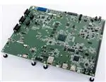
The top and the bottom pictorial views of the EVMK2G are provided in Figure 1 and Figure 2, respectively.
1.4
What's in the Box?
The EVMK2G Kit contains the following parts:
• An on-board, high-speed XDS200 Emulator
• Parts for assembling the LCD and the spacers
• Mini-B to standard A-type USB cable
• Micro-B to standard A-type USB cable
• USB adapters: USB micro-A/B to A socket type adapter
• Ethernet cable
• Female to female RS-232 serial cable (cross cable)
• Micro-SD card 32GB
• SD card reader
• uSD to SD adapter
1.5
What's Not in the Box?
The EVMK2G Kit does not contain the following parts:
• Audio Daughter Card (TI part number AUDK2G)
• Power supply (CUI, Inc., part number SDI65-12-U-P5)
• LCD Touchscreen display (Newhaven Display, Intl., part number NHD-4.3-480272EF-ATXL#-CTP)
10
K2G General Purpose Evaluation Module (EVMK2G)
SPRUI65A – April 2016 – Revised January 2018
Submit Documentation Feedback
Copyright © 2016–2018, Texas Instruments Incorporated
�Introduction
www.ti.com
Figure 1. EVMK2G Board Assembly Pictorial - Top View
BMC
Controller
BMC
LCD
66AK2Gxx
PCIe
SoC
Connector
BMC
JTAG
COM8
Connector
+12 V DC
BMC
UART0
Serial
Expansion
Connector
DCAN0
DCAN1
UART0
Over DB9
Audio
Expansion
Connector
UART2
MiPi 60
Connector
SoC UART0
&
BMC UART0
Over USB
Touch
Connector
LCD
Connector
HDMI
Connector
SPRUI65A – April 2016 – Revised January 2018
Submit Documentation Feedback
MLB
Connector
USB1
Dual Role
RJ45
Ethernet
Connection
Micro SD card
Connector
USB0
Host
Audio
Line In
Mini USB
For XDS200
Audio
Line Out
K2G General Purpose Evaluation Module (EVMK2G)
Copyright © 2016–2018, Texas Instruments Incorporated
11
�Introduction
www.ti.com
Figure 2. EVMK2G Board Assembly Pictorial - Bottom View
NAND
Flash
12
K2G General Purpose Evaluation Module (EVMK2G)
SPRUI65A – April 2016 – Revised January 2018
Submit Documentation Feedback
Copyright © 2016–2018, Texas Instruments Incorporated
�Introduction
www.ti.com
1.6
Acronyms
Table 1 is a description of some terms used in this document.
Table 1. Acronyms
Acronym
Description
ATX
Advanced Technology eXtended
BMC
Board Management Controller
CCS
Code Composer Studio
DDR3
Double Data Rate 3 Interface
DSP
Digital Signal Processor
eHRPWM
Enhanced High-Resolution Pulse Width Modulation
EEPROM
Electrically-Erasable Programmable Read-Only Memory
EMAC
Ethernet Media Access Controller
EMIF
External Memory Interface
EVM
Evaluation Module
EVMK2G
66AK2Gxx General Purpose (GP) Evaluation Module
I2C
Inter-Integrated Circuit
JTAG
Joint Test Action Group
LED
Light-Emitting Diode
McASP
Multichannel Audio Serial Port
MMC
Module Management Controller
PCIe
Peripheral Component Interconnect Express
SoC
System-on-Chip
SPI
Serial Peripheral Interfaces
UART
Universal Asynchronous Receiver/Transmitter
USB
Universal Serial Bus
XDS200
Texas Instruments’ Emulator
2
Testing and Results
2.1
Overview
2.2
Setup
SPRUI65A – April 2016 – Revised January 2018
Submit Documentation Feedback
K2G General Purpose Evaluation Module (EVMK2G)
Copyright © 2016–2018, Texas Instruments Incorporated
13
�Testing and Results
2.3
www.ti.com
Test Points
The EVMK2G board has 187 test points. Each test point and its function is given in Table 2.
Table 2. EVMK2G Test Points
Test
Point Signal
14
Test
Point Signal
Test
Point Signal
Test
Point Signal
9
Reserved for U51
61
DGND
110
LDO5_3V3
160
Reserved for U62.45
13
Reserved for U20B
62
DGND
111
U32-2.G6-GPIO5
161
Reserved for U62.45
14
Reserved for J2
63
VCC12V0_DC_IN
112
NRESPWRON1
162
Reserved for U62.45
15
Reserved for J2
64
VCC12V0_DC_IN
113
PMIC_VDD2
163
Reserved for U62.45
16
Reserved for J2
65
Reserved for U17-4
114
U32-2.EN2
164
MFP2
17
Reserved for J2
66
Reserved for U20A
115
Reserved for U39.A7
165
MFP3
18
Reserved for J2
67
Reserved for U20A
116
U32-2.EN1
166
HDMI_CEC_D
19
Reserved for U20B
68
Reserved for U20A
117
U32-2.GPIO8
167
U96-GPIO2
20
Reserved for U20G.V5
69
Reserved for U20A
118
LDO2_1V8
168
U96-GPIO1
21
Reserved for U20A
70
Reserved for U20A
119
LDO8_3V3
169
LINE2L+
22
Reserved for U20A
71
Reserved for U20A
120
LDO6_3V3
170
LINE2L-
23
Reserved for J2
72
Reserved for U20A
121
LDO7_3V3
171
LED_MODE
25
Reserved for J2
74
Reserved for U20A
122
LDO1_1V8
172
HPLCOM
26
Reserved for J2
75
Reserved for U20A
123
Reserved for U46.A7
173
HPRCOM
29
TPS65000_PG#
76
Reserved for U20A
124
MMC1POW
174
Reserved for J34
30
COM_GPIO9
77
Reserved for U20A
125
Reserved for U1-16.J3
175
U32-2 . GPIO0
31
COM_BTUARTDEBUG
78
Reserved for U20A
126
Reserved for U49.A7
176
BMC_JTAG_TRSTn
33
COM_GPIO10
79
Reserved for U20A
127
SYSCLKOUT
177
Reserved for U17-6
34
COM_GPIO12
80
Reserved for U20A
128
Reserved for U52.A7
178
Reserved for U17-9
35
COM_GPIO11
81
Reserved for U20A
129
DGND
179
Reserved for J34
36
T_TDIS
82
Reserved for U17-4
131
OBSCLK_N
180
Reserved for U20F
37
SPARE0
84
VRTC
132
RMIIREFCLK/
PR0ECAP0ECAP
SYNCOUT
181
Reserved for U20F
38
SPARE1
85
PMIC_PGOOD
133
SoC Reserved pin
182
Reserved for U20B
39
uEXP3
86
Reserved for U20B
135
OBSCLK_P
184
Reserved for U51
40
MEM_A12
88
U32-2 - GPIO3
136
SoC Reserved pin
185
Reserved for U51
41
uEXP2
89
U32-2 - TEST
138
SoC Reserved pin
186
Reserved for U51
42
VCC5V0_DCDC
90
DGND
139
SoC Reserved pin
187
Reserved for U51
43
Reserved for U17-1
91
U32-2.C6-TRAN
140
SoC Reserved pin
189
Reserved for U51
44
uEXP1
92
DGND
141
SoC Reserved pin
191
Reserved for U51
45
Reserved for U17-1
93
Reserved for U20-L
142
SoC Reserved pin
192
Reserved for U51
46
uEXP0
94
Reserved for U20-L
143
SoC Reserved pin
193
BUF_McASP2ACLKX
47
Reserved for U17-1
95
Reserved for U20-L
144
SoC Reserved pin
194
VCC3V3_DC_CONN
48
Reserved for U17-6
96
Reserved for U20-L
145
SoC Reserved pin
195
VCC3V3
49
Reserved for U17-1
97
XOSC1
146
SoC Reserved pin
196
VCC1V2_XDS
50
Reserved for U17-6
98
BMC_HIBn
147
SoC Reserved pin
197
VCC1V8_XDS
51
U18 SS/TR
100
LDO4_1V8
149
SoC Reserved pin
198
VCC3V3_XDS
52
5V_PWRGD
101
CLK32KOUT
150
SoC Reserved pin
199
VCC3V3_DCIN
53
U18.8-COMP
102
U32-2.D5-EN
151
SoC Reserved pin
200
3V3_DCIN_PG
54
Reserved for U20B
103
LDO3_1V8
152
VLED+
201
DGND
55
3V3_CONN_PG
104
DGND
153
DDR_ODT1
202
DGND
56
Reserved for U20J.A4
106
Reserved for U27.A7
154
DDR_CKE1
203
DGND
57
Reserved for
U17-5.T19
107
U32-2.F6-GPIO1
155
DDR_CE1Z
204
DGND
K2G General Purpose Evaluation Module (EVMK2G)
SPRUI65A – April 2016 – Revised January 2018
Submit Documentation Feedback
Copyright © 2016–2018, Texas Instruments Incorporated
�System Description
www.ti.com
Table 2. EVMK2G Test Points (continued)
Test
Point Signal
Test
Point Signal
Test
Point Signal
Test
Point Signal
58
Reserved for U20A
108
U32-2.H7-GPIO4
157
SOC_DSS_FID
205
BUF_McASP2FSX
59
Reserved for U20A
109
U32-2.G8-VREF
158
Reserved for U62.45
206
BUF_MCASP2AXR2
159
SOC_SPI3_MISO
207
BUF_MCASP2AXR3
208
HDMI_AUDD0
209
HDMI_AUDD1
210
HDMI_AUDD2
211
HDMI_AUDD3
212
HDMI_AUDMCLK
213
HDMI_AUDBCLK
214
HDMI_AUDFSX
3
System Description
3.1
Functional Block Diagram
The functional block diagram of the EVMK2G is shown in Figure 3.
3.2
Basic Operation
The EVMK2G is a full-featured general-purpose development tool for the 66AKGxx Keystone II-based
SoC. It supports a comprehensive software including the Texas Instruments Code Composer Studio™
(CCS) integrated development environment (IDE) and Processor Software Development Kit (SDK). The
Processor SDK is a unified software platform for TI embedded processors providing easy setup and fast
out-of-the-box access to benchmarks and demos.
The Processor SDK for the EVMK2G can be downloaded from Processor SDK for 66AK2Gx Processors Linux and TI-RTOS Support.
The latest version of CCS can be downloaded from Code Composer Studio (CCS) Integrated
Development Environment (IDE). It is recommended to use CCS revision 6.1.2 or later with the EVMK2G.
The Processor SDK Linux images are preprogrammed to the SD Card that is shipped with the EVMK2G.
Refer to the Processor SDK user guide for more details on running Linux with the EVM.
Refer to documentation available at Processor SDK for 66AK2Gx Processors - Linux and TI-RTOS
Support for instructions on setting up CCS and exploring software packages delivered with the EVMK2G.
NOTE:
For TI RTOS users, refer to the Processor SDK RTOS Getting Started Guide.
SPRUI65A – April 2016 – Revised January 2018
Submit Documentation Feedback
K2G General Purpose Evaluation Module (EVMK2G)
Copyright © 2016–2018, Texas Instruments Incorporated
15
�System Description
www.ti.com
Figure 3. EVMK2G Functional Block Diagram
To DSS-UL connectors,
due to pin muxing.
Need isolation in
between.
Serial expansion header
MIPI Connector
Micrel
KSZ9031RNX
MDIO
NSS (RGMII)
MiniUSB
XDS200
JTAG
EMU[19:0]
NSS (MDIO)
GPIO / EMU[19:2]
JTAG / EMU Muxes /
Buffers
CPTS
SPI3 to 1588 circuit
DSS-UL
CP2105
To BMC
I2C0
I2C1
I2C2
To PMIC
Temperature
Sensor
To AIC3106
uSDCard
MMC0 (3.3V)
Console header
MAX3221
UART0
To K2G SOC
I2C1
14-pin header
JTAG
PH[3:0]
BMC
I2C0
SYSCLK
USB0_CLK
USB1_CLK
Resets /
Boot
Isolator
DIP Switch Bank (4)
PB Switch Bank (4)
24 MHz Xtal
BMC, WARM,
FULL RESETS
SYSOSC
22.5792 MHz Xtal
LED x4
UART1 Rx
GPIO
McASP2
UART1
Level
shifter
SN74AVC4T245PWR
PCI CE Reference Clock
MT41K512M8RH (qty 5)
DSS
PJ0, PJ1, RSTn
SoC UART2 Tx
COM8
connector
DDR3 EMIF
(x36)
DDR3 devices
NOTE: all port
numbers within the
BMC block are BMC
port numbers, not
SoC port numbers.
Kingston
eMMC
1x PCIe Card-Edge
Connector
PCIe
CP2105
MT29F2G16ABA
USB2.0
Micro-AB
USB1 t 2.0pair
McASP0
Resistor MUX
USB2.0
Type A socket
USB0 t 2.0pair
McASP2
McASP1
MINI USB
NAND (x16) Flash
Quad SPI
512 Mbit
S25FL512S
QSPI
MMC1 (1.8V)
To COM8
To DB-9
CAN xcvr
SN65HVDA54
To 2-pin
header
GPMC
SmartReflex
To DSS-UL
touch screen
connector
SN65HVDA54
DCAN1
GPIOs
To DB-9
CAN xcvr
To 2-pin
header
Mini
USB
I2C EEPROM
I2C to GPIO
expander
TCA9555RTWR
HDMI
Type A
SiI902
2A
Samtec
QSH-020-01-L-D-DP-A
McBSP
Audio
expansion
header
I2C1,
GPIO
DCAN0
UART0
UART1
UART2
Console header
3.5mm
stereo jacks
McASP0 from
Expansion
Connector
Switch
MLB
66AK2Gxx
SoC
SPI
NOR FLASH
To COM8
To BMC
LCD, touch
connectors
SPI0
SPI1
SPI2
SPI3
I2C1
AIC310
6
McASP2
eCAP0, 1
eHRPWM3, 4, 5
eHRPWM0, 1, 2
eQEP
To DSS-UL connectors, due to
pin muxing.
RS232
I2C1
JTAG / EMU[1:0]
Timer 0
Timer 1
DB9
Conn
CS2000
RJ45
25 MHz PHY can also be clocked
Xtal
from RMII_CLK output
pin.
AUDIOOSC
16x2 LCD character display
Y4
Y5
CDCM620
8
Y2
Y3
24 MHz (LVCMOS)
100 MHz (LVDS)
DDRCLK
PCIECLK 100 MHz (CML)
CPTSREFCLK 250 MHz (LVDS)
Y6
Y7
20 MHz
TCVCXO
Rakon
E6718LF
1588
DAC
DAC8550
SPI3
24MHz XO
100 MHz (HCSL)
To INA226 x5
I2C2
PMIC t TPS659118 or TPS65911N
SPI1
24 MHz (LVDS)
DUT Adj. Supply
#1
AVS Core /
_ s _
(+0.9V)
DUT Adj. Supply
#2
DSP Core Fixed
Core / ^ s 1"
(+0.9V)
DUT Adj. Supply
#3
^ s 18_
DSP IO / PLL
(+1.8V)
INA226
INA226
INA226
DUT Adj. Supply
#4
^ s 33_
DSP IO
DUT Adj. Supply
#5
^ s _ Z_
(+1.35V)
(+3.3V)
INA226
INA226
LP2996A
DUT Fixed Supply
³''595()667/´
DDR VTT
(+0.675V)
TLV70708
SERDES L.V. Supply
^> K_PCIE/USB_ W_
(+0.85V)
To 5 pin
header/BMC
Copyright © 2018, Texas Instruments Incorporated
16
K2G General Purpose Evaluation Module (EVMK2G)
SPRUI65A – April 2016 – Revised January 2018
Submit Documentation Feedback
Copyright © 2016–2018, Texas Instruments Incorporated
�System Description
www.ti.com
3.3
Over Voltage Protection Circuit
The Voltage Protection Circuit on the EVMK2G protects the board from over voltage, under voltage,
transient voltage, and reverse voltage input cases. The safe operation input voltage range is 11v to 13v.
Any voltage not in this range is considered a fault and the voltage protection circuit (Figure 4) isolates the
board from this input. LED LD14 (Figure 5) indicates if the DC input applied to board is in a safe input
range.
Figure 4. Over Voltage Protection Circuit
J3
VINPUT
SW1
Q20
VCC12V0_DC_IN
SUM60N10-17-E3
D3
1
3
2
3
5A
2
1
2
2
1
4
3
1
F2
C827
2
4
7
1
R920
47K _1%
R921
47K _1%
PGD
D19
S1G-13-F
C826
0.1uF
8
OUT
GATE
9
10
GATE
UVLO
TIMER
NPGD
LD9
598-8170-107F
VINPUT
R922
EN
5
100K
2
LM5060MM
22uF
2
2
VIN
OVP
1
2
22uF_100V
SENSE
GND
1
+
3
RED
R30
1K
C2
+
6
1
1
D17
C825
SMCJ64CA
LD15
598-8110-107F
DGND
U149
R892
0E
0.01uF
DNI
DGND
R919
237K_1%
GATE
100uF_35V
R917
5.62k_1%
R918
261K_1%
C23
500ASSP3M2QE
C824
0.1uF
1
CON_PWRJACK3_RAPC722
B540C-13-F
R926
10K
DGND
DGND
DGND
DGND
DGND
DGND
DGND
DGND
DGND
DGND
DGND
Note:VINPUT
Vinput nominal = 12V
I input max = 5A
Condition
Reverse Voltage
VCC12V0_DC_IN
LED Status(LD15)
J50
1
2
ON
HDR_2X1
Copyright © 2016, Texas Instruments Incorporated
Figure 5. Fault Indication Circuit
VINPUT
VINPUT
R923
RED
LD14
2
Condition
R925
100 K
1
3
10 K
Q19
R924
598-8110-107F
1
1
10 K
D18
BZT52C13S
2
DGND
OFF
PGD
2
BSS138
VINPUT between 11 to 13V
&
Current below 5A
LED Status(LD14)
VINPUT above 13V or below 11V
&
Current above 5A
ON
DGND
Copyright © 2016, Texas Instruments Incorporated
SPRUI65A – April 2016 – Revised January 2018
Submit Documentation Feedback
K2G General Purpose Evaluation Module (EVMK2G)
Copyright © 2016–2018, Texas Instruments Incorporated
17
�System Description
3.4
www.ti.com
JTAG Emulation Overview
The EVM supports two types of Emulation: On-Board-XDS200 emulator and 60-pin MIPI Header.
When external emulator is not connected to MIPI 60-pin connector, On-board XDS200 embedded JTAG
emulator is the default type of emulation (SoC JTAG signals are routed to XDS200 on-board emulator).
When external emulator is connected to MIPI 60-pin header, it is automatically detected and SoC JTAG
signals are routed to external emulator.
3.4.1
On-Board XDS200 Emulator
The EVMK2G has on-board XDS200 embedded JTAG emulation circuitry. Hence user does not require
any external emulator to connect EVM with Code Composer Studio (CCS). You can connect the target
SoC in the EVM to CCS through the USB cable supplied in the EVM kit.
3.4.2
MIPI 60-pin Header for Connecting External Emulator
In case you want to connect an external emulator to the EVM, the MIPI 60-pin JTAG header is provided
on-board for high-speed real-time emulation. All JTAG and EMUx signals are terminated on the MIPI 60pin header.
The MIPI 60-pin JTAG header supports all standard (XDS510 or XDS560) TI DSP emulators. Refer to the
documentation supplied with your emulator for connection assistance.
EMU pins are pin muxed with DSS (Display Subsystem) and Boot mode pins. The EMU signals are
resistor muxed with DSS signals. A Boot mode buffer is enabled during boot-up to latch the Boot mode
signals.
Resistor muxing between display and trace functionality is shown in Figure 6 and Table 3.
Figure 6. Display and Trace Resistor Multiplexing
RA8
20
20
20
20
20
20
20
20
0E
8
7
6
5
4
3
2
1
SOC_DSSDATA20
SOC_DSSDATA18
SOC_DSSDATA21
SOC_DSSDATA23
SOC_DSSDATA16
SOC_DSSDATA22
SOC_DSSDATA17
SOC_DSSDATA19
RA18
9
10
11
12
13
14
15
16
DNI
8
7
6
5
4
3
2
1
20
20
20
20
20
20
20
20
BUFF_DSSDATA20
BUFF_DSSDATA18
BUFF_DSSDATA21
BUFF_DSSDATA23
BUFF_DSSDATA16
BUFF_DSSDATA22
BUFF_DSSDATA17
BUFF_DSSDATA19
10E
9
10
11
12
13
14
15
16
MIPI_EMU06
MIPI_EMU08
MIPI_EMU03
MIPI_EMU09
MIPI_EMU02
MIPI_EMU04
MIPI_EMU07
MIPI_EMU05
RA9
8
7
6
5
4
3
2
1
SOC_DSSDATA12
SOC_DSSDATA13
SOC_DSSDATA15
SOC_DSSDATA10
SOC_DSSDATA14
SOC_DSSDATA11
SOC_DSSDATA9
SOC_DSSDATA8
RA19
RA7
4
3
2
1
0E
5
6
7
8
0E
9
10
11
12
13
14
15
16
DNI
8
7
6
5
4
3
2
1
20 SOC_DSSDATA7
20 SOC_DSSDATA6
20 SOC_DSSDATA5
20 SOC_DSSDATA4
19
19
19
19
19
19
19
19
BUFF_DSSDATA12 19
BUFF_DSSDATA13 19
BUFF_DSSDATA15 19
BUFF_DSSDATA10 19
BUFF_DSSDATA14 19
BUFF_DSSDATA11 19
BUFF_DSSDATA9 19
BUFF_DSSDATA8 19
10E
9
10
11
12
13
14
15
16
MIPI_EMU17
MIPI_EMU16
MIPI_EMU14
MIPI_EMU11
MIPI_EMU15
MIPI_EMU10
MIPI_EMU12
MIPI_EMU13
BUFF_DSSDATA7
BUFF_DSSDATA6
BUFF_DSSDATA5
BUFF_DSSDATA4
19
19
19
19
DNI
RA171
2
3
4
8 10E
7
6
5
MIPI_EMU18
MIPI_EMU19
Copyright © 2016, Texas Instruments Incorporated
18
K2G General Purpose Evaluation Module (EVMK2G)
SPRUI65A – April 2016 – Revised January 2018
Submit Documentation Feedback
Copyright © 2016–2018, Texas Instruments Incorporated
�System Description
www.ti.com
Table 3. Display and Trace Resistor Multiplexing
DNI
Mount
RA17, RA18, RA19
RA7, RA8, RA9
Description
RA7, RA8, RA9
RA17, RA18, RA19
For HDMI/LCD display (default)
For Trace
The JTAG interface, on-board XDS200 emulator, MIPI 60-pin header for external emulator connection
details are shown in Figure 7.
Figure 7. JTAG Interface Block Diagram
EMU [00:01]
FET SWICH
2
EMU [02:19]
RESISTOR
MUX
18
BUFFER
K2G SoC
6
MIPI - 60
6
FET
SWITCH
JTAG
SIGNALS
JTAG
SIGNALS
6
6
CPLD
BUFFER
CPLD
I/Os
JTAG
SIGNALS
SPI1 6
AM1802
PROCESSOR
CONTROL
SIGNALS
8
SPI FLASH
A0-11
12
DQ0-15
BA0-1
18
SD RAM
Copyright © 2016, Texas Instruments Incorporated
SPRUI65A – April 2016 – Revised January 2018
Submit Documentation Feedback
K2G General Purpose Evaluation Module (EVMK2G)
Copyright © 2016–2018, Texas Instruments Incorporated
19
�System Description
3.5
www.ti.com
Board Management Controller (BMC)
The Tiva™ C Series ARM® Cortex®-M4 microcontroller TM4C129XNCZAD is used as a board
management controller for the EVMK2G. The BMC controls the SoC boot sequence and displays the
status on the character LCD interfaced to the BMC. The BMC facilitates the selection of Boot mode, reset
settings, and configuring clock generators.
The JTAG interface is provided to access and program the BMC controller. Note that the BMC is used
mainly for EVM test automation and, in general, is not required for customer products.
The push buttons, DIP switches, and LEDs are connected to the BMC by way of GPIOs. The 4-bit DIP
switch is used to set the processor boot mode, the three push buttons are for reset, and the remaining are
user configurable.
Isolators are used between the BMC and SoC peripherals. The BMC is interfaced to the SoC through
I2C1 and UART1. The BMC I2C0 is interfaced to the INA devices for processor current monitoring. The
BMC UART0 is muxed between the 4-pin header through RS-232 level translator and the CP2105 for
console purpose.
Table 4. Muxing Between BMC UART1 and SOC_UART2
Signal
BMC_UART_SEL
Logic
SoC UART 2 Connected To
High
UART2 header (J49)
Low
BMC
Table 5. Muxing Between BMC UART0 to USB and 4-pin Header
Signal
BMC_UART0_DETECT
20
Logic
BMC_UART0 Pins Connected To
High
USB-to-UART module CP2105
Low
BMC console 4-pin header (J6)
K2G General Purpose Evaluation Module (EVMK2G)
SPRUI65A – April 2016 – Revised January 2018
Submit Documentation Feedback
Copyright © 2016–2018, Texas Instruments Incorporated
�System Description
www.ti.com
The BMC is powered from 12V through the LM22675 DC-DC regulator. The connection details are shown
in Figure 8.
Figure 8. Board Management Controller (BMC) Block Diagram
12V
12 V
DC_DC
TPS54429ERSAREN
12V
DC-DC
LM22675
3.3V
EN
LCD
128 X 32
Pixels
DIP
Switch
DC_DC
TPS54429ERSAR
3.3V
CVDD
CVDD1
DVDD_DDR
PMIC
SPI1
I2C2
I2C1
I2C0
Buffer
4
K2G SoC
I2C0
Buffer
GPIOs
INA226 x5
5 Pin HDR
2
LED
UART0
MAX3221
4 Pin HDR
CP2105
Mini- USB
GPIOs
BMC
16
SPI0
BOOT MODE SIGNALS
Isolator
CDCM6208
DSS[8:23]
ISOLATOR x4
SOC,
DEVICES
RESET &
CTRL
Signals
UART1
23 GPIOs
UART2
MUX/Buffer
BMC_INT
INT1
SoC_INT
Isolator
INT
JTAG Lines
GPIOs
JTAG
14 Pin
Connector
BMC_RESETn
5
Push
Button
x6
Copyright © 2016, Texas Instruments Incorporated
SPRUI65A – April 2016 – Revised January 2018
Submit Documentation Feedback
K2G General Purpose Evaluation Module (EVMK2G)
Copyright © 2016–2018, Texas Instruments Incorporated
21
�System Description
3.6
www.ti.com
Clock Distribution
The EVMK2G has the following clock sources, crystals, and oscillators.
• 66AK2Gxx SoC clocks (see Figure 9):
– Y5: 22.579 MHz Audio clock for SoC
– Y6: 24 MHz System clock to the SoC
– Y7: 12.28 MHz to CS2000
– Y8: 24 MHz Secondary Reference for clock generator
– U62: CDCM clock generator
• Other clocks (see Figure 10):
– Y1: 32.768 kHz to AM1802 XDS
– Y2: 24 MHz System clock to AM1802 XDS
– Y3: 25 MHz Clock to BMC Controller
– Y4: 32.768 kHz Real-Time Clock (RTC) to Power Management IC (TPS659118)
– Y9: 25 MHz Clock for Ethernet PHY
– U21: 32.768 kHz Real-Time Clock (RTC) to BMC
– U75: 12.28 MHz Oscillator for audio clocks
Figure 9. 66AK2Gxx SoC Clocks Block Diagram
AUDOSC_IN
SYSCLOCK
Y5
CPTS_REFCLK
AUDOSC_OUT
24 MHz
250 MHz
CDCM6208
24 MHz
Y8
100 MHz
SYSOSC_IN
DDR_CLK
Y6
PCIe_CLK
100 MHz
SYSOSC_OUT
PCIe_CLK_100MHz
K2G SoC
PCIe x1 Connector
CPTS_TS_COMP
McASP2AHCLK
CLKOUT
CLKIN
CS2000
Y7
Copyright © 2016, Texas Instruments Incorporated
22
K2G General Purpose Evaluation Module (EVMK2G)
SPRUI65A – April 2016 – Revised January 2018
Submit Documentation Feedback
Copyright © 2016–2018, Texas Instruments Incorporated
�System Description
www.ti.com
Figure 10. Other Clocks Block Diagram
Y4
PMIC
Y9
KSZ9031RNX
Y3
BMC
32.768 kHz
Audio Codec
12.288MHz
HDMI TX
Y2
AM1802
Y1
Copyright © 2016, Texas Instruments Incorporated
SPRUI65A – April 2016 – Revised January 2018
Submit Documentation Feedback
K2G General Purpose Evaluation Module (EVMK2G)
Copyright © 2016–2018, Texas Instruments Incorporated
23
�System Description
3.7
www.ti.com
DDR3L Interface
The 66AK2Gxx SoC supports ×36 bit (32-bit data + 4-bit ECC) DDR3L. Four 4-Gbit (512M × 8) DDR3L
chips (MT41K512M8RH-125) from Micron are used to obtain a memory size of 2GByte and one DDR3L
chip is interfaced to the ECC data bus CB00-CB03, CBDQS, and CBDQM. The DDR3L chips are routed
as per Fly-by topology as shown in Figure 11.
Figure 11. DDR3L Interface Block Diagram
1.35V
CBDQM
DVDD_DDR
CBDQS
CB00-CB03
DQM3
DQS3
DQ24-DQ31
DQM2
DQS2
K2G SoC
DQ16-DQ23
DQM1
DQS1
DQ8-DQ15
DQM0
DQS0
DQ0-DQ7
BA0-BA2
A0-A15
CAS#
RAS#
CE0#
CKE0#
ODT0
RESET#
WE#
DDR3CLK0
DDR3L
MT41K512M8RH
-125:E
DDR3L
MT41K512M8RH
-125:E
DDR3L
MT41K512M8RH
-125:E
DDR3L
MT41K512M8RH
-125:E
DDR3L
MT41K512M8RH
-125:E
Copyright © 2016, Texas Instruments Incorporated
24
K2G General Purpose Evaluation Module (EVMK2G)
SPRUI65A – April 2016 – Revised January 2018
Submit Documentation Feedback
Copyright © 2016–2018, Texas Instruments Incorporated
�System Description
www.ti.com
3.8
NAND Flash
2-Gbit NAND Flash (MT29F2G16ABA) from Micron with a 16-bit data width is interfaced to the processor
GPMC (General-Purpose Memory Controller) interface. The NAND Flash is interfaced to GPMC chip
select 0.
The connection details are as shown in Figure 12. The operating voltage of the GPMC interface and
NAND flash is 3.3v.
Figure 12. NAND Flash Block Diagram
3.3 V
GPMC_AD [0:15]
I/O
GPMC_ADVn_ALE
ALE
GPMC_BEn0_CLE
CLE
GPMC_OEn_REN
#RE
K2G SoC
GPMC_WEn
#WE
NAND FLASH
MT29F2G16ABA
GPMC_WPn
#WP
GPMC_CSn0
#CE
GPMC_WAIT0
R/B#
Copyright © 2016, Texas Instruments Incorporated
SPRUI65A – April 2016 – Revised January 2018
Submit Documentation Feedback
K2G General Purpose Evaluation Module (EVMK2G)
Copyright © 2016–2018, Texas Instruments Incorporated
25
�System Description
3.9
www.ti.com
SPI Flash
The SPI Flash (N25Q128A13ESFESF40F) from Micron is a 128-Mbit Serial Flash interfaced as shown in
Figure 13. The Serial Flash is interfaced to the SPI1 port of the processor and is connected to chip
select 0.
The write protection for the Flash is controlled by the BMC. The Hold signal (to pause the serial
communication without deselecting the device) is connected to SoC GPIO with a default pull-up.
Figure 13. SPI Flash Block Diagram
3.3 V
SPI1_CLK
C
SPI1_MISO
Q
SPI1_MOSI
D
K2G SoC
SPI1_CSn0
#S
SPI FLASH
N25Q128A13ESF40F
GPIO
#HOLD
#W
RESET#
FLASH_WP#
BMC
FLASH_RESET#
AND GATE
SOC_RESETSTATz
Copyright © 2016, Texas Instruments Incorporated
26
K2G General Purpose Evaluation Module (EVMK2G)
SPRUI65A – April 2016 – Revised January 2018
Submit Documentation Feedback
Copyright © 2016–2018, Texas Instruments Incorporated
�System Description
www.ti.com
3.10 Quad SPI (QSPI) Flash
The Quad SPI (QSPI) Flash is a 512-Mbit device (S25FL512S) from Spansion interfaced as shown in
Figure 14. The reset signal for the QSPI Flash is connected to the BMC. The Quad SPI Flash is interfaced
to chip select 0 of the QSPI interface on the processor.
Figure 14. Quad SPI (QSPI) Flash Block Diagram
3.3 V
QSPI_RCLK
QSPI_CLK
SCK
QSPI_CSn0
K2G SoC
CS#
QSPI_D0
QSPI_D1
I/O0
I/O1
QSPI_D2
I/O2
QSPI_D3
QSPI FLASH
S25FL512S
I/O3
RESET#
QSPI_RSTn
BMC
AND GATE
SOC_RESETSTAT
Copyright © 2016, Texas Instruments Incorporated
3.11 EEPROM
The Atmel AT24CM01 provides 1Mb of Serial Electrically-Erasable and Programmable Read-Only
Memory (SEEPROM). This is interfaced to I2C0 port of the processor as shown in Figure 15. The device
address is set by the two address pins A1 and A2 that are connected to ground to give a 7-bit address
0x50. The Write protect pin of the EEPROM is connected to a GPIO of the BMC.
Figure 15. EEPROM Interface Block Diagram
3.3 V
I2C2_SCL
SCL
K2G SoC
I2C2_SDA
SDA
EEPROM
AT24CM01
EEPROM_WP
BMC
WP
Copyright © 2016, Texas Instruments Incorporated
SPRUI65A – April 2016 – Revised January 2018
Submit Documentation Feedback
K2G General Purpose Evaluation Module (EVMK2G)
Copyright © 2016–2018, Texas Instruments Incorporated
27
�System Description
www.ti.com
3.12 SD Card
Micro SD Card connector is connected to MMC0 interface of the processor as shown in Figure 16. ESD
protection circuits are included for all the connector pins that are prone to ESD. Refer to Section 6.12 for
SD Card connector pin outs.
Figure 16. SD/MMC Interface Block Diagram
3.3 V
K2G SoC
MMC0_CLK
MMC0_CMD
MMC0_D [0-3]
MMC0_SDCD
CLK
CMD MICRO
D[0-3] SD CARD
CONN
CD
ESD
DIODES
Copyright © 2016, Texas Instruments Incorporated
3.13 eMMC
The eMMC flash chip from Kingston (16GB) is interfaced with MMC1 of the processor as shown in
Figure 17. MMC1 is muxed between the eMMC Flash and the COM8 connector. By default, MMC1 is
connected to eMMC.
Resistor muxing between eMMC and COM8 is shown in Figure 18 and Table 6.
Figure 17. eMMC Interface Block Diagram
MMC1_CLK
MMC1_CMD
MMC1_D [0-8]
CLK
eMMC
CMD
D [0-8] (eMMC16G-S100)
K2G SoC
MMC1_D [0-4]
MMC1_CMD
MMC1_CLK
COM8
Connector
Copyright © 2016, Texas Instruments Incorporated
28
K2G General Purpose Evaluation Module (EVMK2G)
SPRUI65A – April 2016 – Revised January 2018
Submit Documentation Feedback
Copyright © 2016–2018, Texas Instruments Incorporated
�System Description
www.ti.com
Figure 18. eMMC and COM8 Resistor Multiplexing
U1-8
GPIO0_108/MCASP2AXR0
GPIO0_109/MCASP2AXR1
GPIO0_110/MCASP2AXR2
GPIO0_111/MCASP2AXR3
GPIO0_112/MCASP2AXR4
GPIO0_113/MCASP2AXR5
McASP2
GPIO0_119/MCASP2AHCLKX
GPIO0_120/MCASP2ACLKX
GPIO0_118/MCASP2FSX
GPIO0_116/MCASP2AHCLKR
GPIO0_114/MCASP2ACLKR
GPIO0_115/MCASP2FSR
XREFCLK/GPIO0_117/MCASP2AMUTE
D3
A2
E4
B1
A3
E5
SOC_MCASP2AXR0 R428
0E_1%
R423
0E_1% SOC_MCASP2AXR1
R433
0E_1% SOC_MCASP2AXR2
R415
0E_1% SOC_MCASP2AXR3
R396
0E_1% SOC_MCASP2AXR4
R420
0E_1% SOC_MCASP2AXR5
D5
B3
C3
R417
R413
R411
0E_1% SOC_McASP2AHCLKX
0E_1% SOC_McASP2ACLKX
0E_1% SOC_McASP2FSX
E6
B2
D4
R407
R401
R409
0E_1% SOC_McASP2AHCLKR
0E_1% SOC_McASP2ACLKR
0E_1% SOC_McASP2FSR
C2
SOC_MCASP2AMUTE R393
DNI
SoC_LED0 34
SOC_MCASP2AXR1 23
SOC_MCASP2AXR2 23
SOC_MCASP2AXR3 23
SOC_MCASP2AXR4 23
SOC_McASP2ACLKX 23
SOC_McASP2FSX 23
SOC_McASP2AHCLKR
0E_1% WLAN_TRANS_EN
36
23,29
66AK2G02
MMC1
MMC1DAT0/GPIO0_66
MMC1DAT1/GPIO0_65
MMC1DAT2/GPIO0_64
MMC1DAT3/GPIO0_63
MMC1DAT4
MMC1DAT5/GPIO0_61
MMC1DAT6
MMC1DAT7/GPIO0_59
MMC1CLK /GPIO0_67
MMC1CMD
MMC1POW
MMC1SDCD/GPIO0_69
MMC1SDWP/GPIO0_70
R388
R387
0E_1%
0E_1%
K2
SMD
TP124
J3
SMD
TP125
10K_1%
10K_1%
10K_1%
R286
R271
10K_1%
R299
R304
SOC_MMC1_DAT0_R
SOC_MMC1_DAT1_R
SOC_MMC1_DAT2_R
SOC_MMC1_DAT3_R
10K_1%
SOC_MMC1_CLK
SOC_MMC1_CMD
0E
8
7
6
5
10K_1%
J4
J2
RA6
1
2
3
4
R269
SOC_MMC1_DAT0
SOC_MMC1_DAT1
SOC_MMC1_DAT2
SOC_MMC1_DAT3
SOC_MMC1_DAT4
SOC_MMC1_DAT5
SOC_MMC1_DAT6
SOC_MMC1_DAT7
10K_1%
H3
F5
J5
H4
E3
G4
F4
G5
R281
U1-16
0E_1% SOC_MCASP2AXR0_R
0E_1% SOC_MCASP2AMUTE_R
R292
SOC_MCASP2AXR0
R821 DNI
SOC_MCASP2AMUTE R822 DNI
SOC_MMC1_CLK_R
SOC_MMC1_CMD_R
DNI
K3
SOC_MMC1_SDWP
66AK2G02
R676
1K
R347
0E_1%
17
TRANS_EMMC_RSTn
R267
DGND
NOTE: MMC1 IS BY DEFAULT CONNECTED TO EMMC. IF COM8 TO BE USED RESISTOR RA6, R387 AND R822
SHOULD BE DNI AND RQZZ+15, R713, R714 & R393 SHOULD BE MOUNTED
SOC_MMC1_CLK
SOC_MMC1_CMD
R713
R714
DNI
DNI
0E_1%
0E_1%
BUF_MMC1_CLK 23
BUF_MMC1_CMD 23
DNI
RA15 1
2
3
4
SOC_MMC1_DAT0
SOC_MMC1_DAT1
SOC_MMC1_DAT2
SOC_MMC1_DAT3
8 0E
7
6
5
BUF_MMC1_DAT0
BUF_MMC1_DAT1
BUF_MMC1_DAT2
BUF_MMC1_DAT3
23
23
23
23
Table 6. eMMC and COM8 Resistor Multiplexing
DNI
Mount
RA6, R387, R388, and R822
RA15, R713, R714, and R393
Connect MMC1 to COM8
RA15, R713, R714, and R393
RA6, R387, R388, and R822
Connect MMC1 to eMMC (default)
SPRUI65A – April 2016 – Revised January 2018
Submit Documentation Feedback
Description
K2G General Purpose Evaluation Module (EVMK2G)
Copyright © 2016–2018, Texas Instruments Incorporated
29
�System Description
www.ti.com
3.14 Gigabit Ethernet
The Gigabit Ethernet PHY (KSZ9031RNX) from MICREL is interfaced to the RGMII port of the processor
as shown in Figure 19.
The RJ45 connector with magnetics is interfaced to the MDI (media dependent interface) port of PHY. The
PHY address, PHYAD [2:0], is sampled and latched at power-up/reset and is configurable to any value
from 0 to 7. Each PHY address bit is configured as:
• Pull-up = 1
• Pull-down = 0
The MODE [3:0] pins are sampled and latched at power-up/reset. Each Mode bit is configured as:
• Pull-up = 1
• Pull-down = 0
The MODE pins are set for RGMII mode (10/100/1000 speed half/full-duplex).
Reference clock for PHY is provided by the 25-MHz crystal, Y9. (See Section 3.6)
Figure 19. Gigabit Ethernet Interface Block Diagram
RGMII_TXCLK
TXC
TXRXPA
RGMII_TXCTL
TX_CTL
TXRXMA
RGMII_TXD [0-3]
TD [0-3]
RGMII_RXCLK
RXC
K2G SoC
Gigabit Ethernet PHY
KSZ9031RNX
RGMII_RXCTL
RX_CTL/PHYAD2
RGMII_RXD [0-3]
TXRXPB
TXRXMB
TXRXPC
TXRXMC
RD [0-3] / MODE [0:3]
TXRXPD
MDC
TXRXMD
MDIO_CLK
RJ45
Connector with
Magnetics
LPJG16314A4NL
MDIO_DATA
MDIO
Copyright © 2016, Texas Instruments Incorporated
30
K2G General Purpose Evaluation Module (EVMK2G)
SPRUI65A – April 2016 – Revised January 2018
Submit Documentation Feedback
Copyright © 2016–2018, Texas Instruments Incorporated
�System Description
www.ti.com
3.15 PCIe
The PCIe RX and TX pairs are connected to x1 PCIe edge card connector as shown in Figure 20. Clock
generator (CDCM6208) provides the 100-MHz reference clocks for the PCIe port of the processor and to
the daughter card that connects to the edge card connector.
Figure 20. PCIe Interface Block Diagram
K2G SoC
TXN0
TXP0
RXN0
RXP0
RXN0
RXN0
TXN0
TXP0
PCIE_CLK_P/N
x1 Edge
Card Connector
100MHz
(CML)
CDCM6208
100MHz
(HCSL)
Copyright © 2016, Texas Instruments Incorporated
3.16 Display Interface
The Display interface (DSS) is muxed between the LCD and the HDMI transmitter SiI9022A as shown in
Figure 21. The DSS is muxed using two 32-bit buffers to connect to the LCD or the HDMI transmitter.
Either the LCD or the HDMI transmitter is enabled by switches SW13 and SW14:
• for HDMI: SW13 and SW14 = ON
• for LCD: SW13 and SW14 = OFF
3.16.1
LCD
The TFT LCD module (NHD-4.3-480272EF-ATXL-CTP) from Newhaven display can be plugged into the
40-pin FPC connector on the EVMK2G. The LCD backlight is driven by DC-DC boost-converter
TPS61081DRCT.
The LCD is not part of the EVMK2G kit, it should be purchased separately. More details of LCD
installation procedure is provided in Section 8.
3.16.2
HDMI Transmitter
The EVMK2G supports HDMI interface with the HDMI transmitter SiI9022A. The HDMI signals are
terminated to a connector by way of an ESD protection device TPD12S016PWR. The HDMI interface is
controlled by I2C1 of the SoC. The HDMI signals consist of three differential pairs of data lines and one
differential pair of clock line.
The McASP2 is interfaced to the HDMI transmitter to support audio over HDMI and I2C1 for control.
McASP2TX is shared between the HDMI transmitter and the Audio Codec. The Audio MCLK for the HDMI
transmitter is derived from a 12.288-MHz Oscillator, U75, that is shared between the Audio Codec and the
HDMI transmitter (See Section 3.6).
SPRUI65A – April 2016 – Revised January 2018
Submit Documentation Feedback
K2G General Purpose Evaluation Module (EVMK2G)
Copyright © 2016–2018, Texas Instruments Incorporated
31
�System Description
www.ti.com
Figure 21. Display Interface Block Diagram
LCDDATA [0:23]
DSS_DATA [0:23]
LCD_HSYNC
DSS_HSYNC
DSS_VSYNC
EVMK2G SOC
DSS_PCLK
DSS_DE
SW14
LCD_VSYNC
32 bit
Buffer
S74LVC32244ZKER
LCD Conn
40 pin FPC
Connector
LCD_PCLK
LCD_AC_BIAS_EN
OE#
3.3 V
1.2 V
HDMI DATA
HDMI HSYNC
32 bit
Buffer
S74LVC32244ZKER
HDMI_VSYNC
HDMI
Transmitter
SiI9022A
HDMI_PCLK
HDMI_AC_BIAS_EN
K2G SoC
SW13
OE#
HDMI_CE
HDMI_HPLG
HDMI_I2C
I2C1_SCL
TMDS_TX
TMDS_CL
I2C1_SDA
ESD
TPD12S016
MCASP2_ACLKX
MCASP2_AXR
HDMI_CE
HDMI_HP
TMDS_TX
HDMI
Audio
Selection
MCASP0_ACLKX
HDMI_ I2C
TMDS_CL
MCASP2_AFSX
MCASP0_AFSX
MCASP0_AXR
HDMI Connector
Std Type A
12.288MHz OSC
Copyright © 2016, Texas Instruments Incorporated
Table 7. DSS Lines Between LCD and HDMI Multiplexing
SW13 and SW14 Position
32
Signal
Result
ON
SEL_HDMIn signal is low
HDMI is enabled
OFF
SEL_LCDn signal becomes low
LCD is enabled
K2G General Purpose Evaluation Module (EVMK2G)
SPRUI65A – April 2016 – Revised January 2018
Submit Documentation Feedback
Copyright © 2016–2018, Texas Instruments Incorporated
�System Description
www.ti.com
Table 8. HDMI Audio Line Selection Between McASP0 and McASP2
Signal
Logic
DC_BRD_DET
Result
Low
McASP2 is connected to HDMI Transmitter SiI9022A.
High
McASP0 is connected to HDMI Transmitter SiI9022A.
3.17 Touch Connector
NOTE: The EVMK2G does not come with an LCD Touchscreen display, it should be purchased
separately.
The Touch Connector interface is shown in Figure 22.
Figure 22. Touch Interface Block Diagram
I2C1_SDA
I2C1_SCL
K2G
SoC
TOUCH_INTR
TOUCH
Connector
RST
Copyright © 2016, Texas Instruments Incorporated
3.18 Audio Codec
The Audio Codec TLV320AIC3106IRGZT is interfaced to the McASP2 port of the processor as shown in
Figure 23. The ACLKX and FSX lines of McASP2 are shared between the Audio Codec, COM8, and the
HDMI transmitter. Hence, a buffer with OE# is connected as shown in Figure 23 for muxing. Switch SW15
is turned ON for connecting the McASP2 to the Audio Codec. Audio Line In and Line Out are provided
through 3.5mm audio jacks (J32 and J33).
Figure 23. Audio Codec Interface Block Diagram
HPROUT
MCASP2_ACLKX
HPLOUT
MCASP2_AFSX
K2G SoC
MCASP2_AXR [2:3]
Buffer
AUDIO
CODEC
LINE1R
LINE1L
TLV320AIC
SW15
OE#
Copyright © 2016, Texas Instruments Incorporated
Table 9. Audio Codec Multiplexing
Signal
Switch
AUD_BUFF_EN
SW15 is ON
SOC_McASP2 signals are going to Audio Codec and HDMI transmitter.
COM8_BUFF_EN
SW11 is ON
COM8 signals are connected to SOC_McASP2.
SPRUI65A – April 2016 – Revised January 2018
Submit Documentation Feedback
Output
K2G General Purpose Evaluation Module (EVMK2G)
Copyright © 2016–2018, Texas Instruments Incorporated
33
�System Description
www.ti.com
3.19 COM8 Connector
The COM8 connector interface is generally used to communicate with wireless modules. It can be
connected to a WiLink™ 8 module. A Level Translator SN74AVC4T245PW is used to convert the signals
UART and McASP from 3.3V to 1.8V as shown in Figure 24.
Figure 24. COM8 Connector Interface Block Diagram
MMC1_D [0-3]
MMC1_CMD
MMC1_CLK
SDIO Buffer
TXB0108PWR
WLAN_EN
OE#
UART1_TX
UART1_RX
K2G SoC
COM8
Connector
UART1_CTS
UART1_RTS
Level
Translator
SN74AVC4T245PW
MCASP2_ACLKR
MCASP2_AFSR
MCASP2_AXR [0:1]
Copyright © 2016, Texas Instruments Incorporated
3.20 DCAN
The CAN transceiver ISO1050DUB is connected to DCAN0 and DCAN1 interface of the processor as
shown in Figure 25.
Figure 25. DCAN Interface Block Diagram
DCAN_TX
K2G SoC
DCAN_RX
CAN
Transceiver
ISO1050DUB
DB9
Connector
Copyright © 2016, Texas Instruments Incorporated
34
K2G General Purpose Evaluation Module (EVMK2G)
SPRUI65A – April 2016 – Revised January 2018
Submit Documentation Feedback
Copyright © 2016–2018, Texas Instruments Incorporated
�System Description
www.ti.com
3.21 MLB
The Media Local Bus (MLB) interface signals are terminated in Samtec’s QSH-020-01-L-D-DP-A
connector as shown in Figure 26.
Figure 26. MLB Interface Block Diagram
MLB_PSIGP
MLB_PSIGN
MLB_PDATP
MLB_PDATN
MLB_PCLKP
K2G SoC
MLB
MLB_PCLKN
MLB_CLK
MLB_DAT
MLB_SIG
Copyright © 2016, Texas Instruments Incorporated
SPRUI65A – April 2016 – Revised January 2018
Submit Documentation Feedback
K2G General Purpose Evaluation Module (EVMK2G)
Copyright © 2016–2018, Texas Instruments Incorporated
35
�System Description
www.ti.com
3.22 USB Host
USB0 shall be used for the USB Host interface in the EVMK2G. The USB0ID pin is grounded through a 0ohm resistor in order to configure it as USB Host as shown in Figure 26. Common mode choke coil and
ESD diodes (TPD2EUSB30DRTR) are used on USB data signals. A power distribution switch
(TPS2051BD) is used to deliver USB power to the devices.
Figure 27. USB Host Interface Block Diagram
5V
USB0_VBUS
USB0_VBUS
POWER
SWITCH
USB0_DRVVBUS
K2G SoC
USB0_DP
USB0_DM
EN
Common
Mode
Choke
USB
Type A
USB0_ID
ESD Diodes
(TPD2EUSB30DRTR)
Copyright © 2016, Texas Instruments Incorporated
3.23 USB Dual Role
USB1 shall be configured as the USB Dual Role in the EVMK2G. The USB Dual Role interface is shown
in Figure 28. Common mode choke coil and ESD diodes are used on USB data signals. A power
distribution switch (TPS2051BD) is used to deliver USB power when it acts as a host.
Figure 28. USB Dual Role Interface Block Diagram
USB1_VBUS
5V
USB1_VBUS
POWER
SWITCH
USB1_DRVVBUS
K2G SoC
USB1_DP
USB1_DM
EN
Common
Mode
Choke
USB-OTG
Micro-AB
Connector
USB1_ID
ESD Diodes
(TPD2EUSB30DRTR)
Copyright © 2016, Texas Instruments Incorporated
36
K2G General Purpose Evaluation Module (EVMK2G)
SPRUI65A – April 2016 – Revised January 2018
Submit Documentation Feedback
Copyright © 2016–2018, Texas Instruments Incorporated
�System Description
www.ti.com
3.24 UART
There are three UART ports available in the EVMK2G.
UART0 debug port is multiplexed between the DB9 port, USB-to-UART converter (CP2105), and the
Serial Expansion header as shown in Figure 29.
Table 10. UART0 Multiplexing
Signal
UART0_TXVR_EN
SW12
Logic
ON
Low
SoC UART0 Pins Connected To
DB9 connector via RS-232 chip.
OFF
High
USB-to-UART converter CP2105.
UART1 is connected to the COM8 connector as shown in Figure 30. Connection to COM8 and eMMC is
muxed and is explained in Section 3.13.
Table 11. UART1 Multiplexing
Signal
Logic
WLAN_TRANS_EN
Output
Low
SoC UART1 pins are connected to COM8
High
MMC1 connected
UART2 is muxed between the BMC UART1 and the 6-pin header, as shown in Figure 31 and explained in
Section 3.5.
Figure 29. UART0 Interface Block Diagram
UART0_RTS
UART0_CTS
Serial
Expansion
Connector
K2G SoC
UART0_RX
Buffer
UART
Transceiver
DB9
Connector
UART0_TX
OE#
UART0_TXVR_EN
CP2105_DP
Buffer
USB to UART
CP2105
CP2105_DM
USB
Mini-B
Connector
OE#
SOC_UART0_CP2105_EN
Copyright © 2016, Texas Instruments Incorporated
SPRUI65A – April 2016 – Revised January 2018
Submit Documentation Feedback
K2G General Purpose Evaluation Module (EVMK2G)
Copyright © 2016–2018, Texas Instruments Incorporated
37
�System Description
www.ti.com
Figure 30. UART1 Interface Block Diagram
K2G SoC
UART1_TX
COM_BTUARTRX
UART1_RX
COM_BTUARTTX
UART1_CTSn
Level
Translator
UART1_RTSn
COM_BTUARTRTS
COM8
Connector
COM_BTUARTCTS
WLAN_TRANS_EN
OE#
Copyright © 2016, Texas Instruments Incorporated
Figure 31. UART2 Interface Block Diagram
TX
Buffer
BMC
UART1
RX
OE#
BMC_UART_SEL
K2G SoC
UART2_TX
OE#
TX
RX
Buffer
UART2_RX
6 Pin
Header
Copyright © 2016, Texas Instruments Incorporated
38
K2G General Purpose Evaluation Module (EVMK2G)
SPRUI65A – April 2016 – Revised January 2018
Submit Documentation Feedback
Copyright © 2016–2018, Texas Instruments Incorporated
�System Description
www.ti.com
3.25 Audio Expansion Connector
The EVMK2G consists of an audio expansion connector for an audio daughter card. Audio expansion
connector contains McASP0, McASP1, and McASP2 signals along with the I2C1, SPI2, and GPIO signals
as shown in Figure 32.
Figure 32. Audio Expansion Connector Interface Block Diagram
SCL1
SDA1
McASP0_AXR [0:7], [12-15]
MCASP0_AFSX
MCASP0_ACLKX
MCASP0_AHCLKX
MCASP0_AMUTE
MCASP0_AFSR
MCASP0_ACLKR
MCASP0_AHCLKR
MCASP1_AXR [0:9]
MCASP1_AFSX
MCASP1_ACLKX
K2G SoC
MCASP1_AHCLKX
AUDIO
Expansion
Connector
MCASP1_AFSR
MCASP1_ACLKR
MCASP1_AHCLKR
MCASP2_AXR 5
MCASP2_AFSR
MCASP2_AHCLKR
MCASP2_ACLKR
SPI2_SCS0/SPI2_SCS1
SPI2_CLK
SPI2_SIMO
SPI2_SOMI
GPIO
Copyright © 2016, Texas Instruments Incorporated
SPRUI65A – April 2016 – Revised January 2018
Submit Documentation Feedback
K2G General Purpose Evaluation Module (EVMK2G)
Copyright © 2016–2018, Texas Instruments Incorporated
39
�System Description
www.ti.com
3.26 Serial Expansion Connector
The EVMK2G consists of a Serial Expansion connector that contains I2C0, SPI0, UART0, Timer 0,
Timer1, eHRPWM3, eHRPWM4, eHRPWM5, and eCAP signals as shown in Figure 33.
Figure 33. Serial Expansion Connector Interface Block Diagram
I2C0_SCL
I2C0_SDA
I2C2_SCL
I2C2_SDA
SPI0_SCS0
SPI0_CLK
SPI0_SIMO
SPI0_SOMI
UART0
UART0
TIMI0
TIMO0
TIMI1
K2G SoC
TIMO1
Serial
Expansion
Connector
eHRPWM3_A
eHRPWM3_B
eHRPWM3_SYNCI
eHRPWM3_SYNCO
eHRPWM4_A
eHRPWM4_B
eHRPWM5_A
eHRPWM5_B
eHRPWM_TZn3
eHRPWM_TZn4
eHRPWM_TZn5
ECAP1_IN_PWM1_OUT
Copyright © 2016, Texas Instruments Incorporated
40
K2G General Purpose Evaluation Module (EVMK2G)
SPRUI65A – April 2016 – Revised January 2018
Submit Documentation Feedback
Copyright © 2016–2018, Texas Instruments Incorporated
�System Description
www.ti.com
3.27 I2C Address Mapping
The address mapping for the I2C interface on the EVMK2G is shown in Table 12 and Table 13.
Table 12. SoC Address Table
I2C Used
I2C0
I2C1
I2C2
Device
Address
EEPROM
0x50, 0x51
BMC
0x0 (Programmable)
Serial Expansion Connector
TBD
PCIe Connector
TBD
HDMI Transmitter
0x3B, 0x3F, 0x62
Audio Codec
0x1B
Touch Screen
0x70, 0x71
I/O Expander
0x20
Temperature Sensor
0x48
MLB Connector
TBD
Audio Expansion Connector
0x4A, 0x4B, 0x4C, 0x4D
Clock Generator
0x4F
0x2D (General Purpose)
PMIC
0x12 (Voltage Scaling)
Table 13. BMC I2C Address Table
BMC I2C Used
Device
7-Bit Address
0x40 : 3.3V
0x41 : CVDD
I2C0
PMBUS
0x42 : CVDD1
0x43 : 1.8V
0x44 : DVDD_DDR
I2C1
Processor
SPRUI65A – April 2016 – Revised January 2018
Submit Documentation Feedback
Always Master
K2G General Purpose Evaluation Module (EVMK2G)
Copyright © 2016–2018, Texas Instruments Incorporated
41
�System Description
www.ti.com
3.28 McASP Configuration
Table 14. McASP Configuration
McASP Port
Device
McASP0 RX
I2S Header
I2S Header
McASP0 TX
DAC
McASP0 TX
McASP1 RX
ADC- PCM1865 x2
McASP1 RX
McASP2 TX
McASP2 RX
Clock Master
HDMI Transmitter
McASP2 TX
Audio Codec AIC3106
McASP2 TX
DIR9001
DIR9001
Audio Codec AIC3106
McASP2 Rx (SYNC mode)
COM8
COM8
Figure 34. McASP Interface Block Diagram
AUDIO CODEC
MCASP2_ACLKX
MCASP2_AFSX
MCASP2_AXR2
BCLK
WCLK
BUFFER
MCLK
DIN
DOUT
M
c
S
MCASP2_AXR1
MCASP2_AXR4
P
MCASP2_AXR3
BUFFER
AUD_CLK
AUD_FSYNC
AUD_DIN
AUD_DOUT
COM8
A
MCLK
SCK
WS
SD[0:3]
HDM TXR
MUX 2
12.288MHz
OSC
4
2
MCASP2_AXR5
MCASP2_AHCLKR
BCKO
BUFFER
MCASP2_AFSR
LRCKO
DOUT
SCKO
DIR9001
MCASP2_ACLKR
A
CS2000
U
DOUT1
DOUT2
4
S
P
MCASP1_AXR9
1
MCASP1_AHCLKX
4
BUFFER
G
T
BUFFER
E
MUX
DIN[1:4]
BCK
LRCK
SCKI
MUTE
MUTE
SCKI
BCK
LRCK
DIN[1:4]
4
4
4
R
C
A
R
D
DNI
MCASP0_AHCLKR
MCASP0_ACLKR
MCASP0_AFSR
MCASP0_AXR[12:15]
4
4
0
4
JUMPER
BUFFER
OE#
JUMPER
BUFFER
OE#
MCLKOUT
BCLKOUT
LRCKOUT
DOUT[0:3]
MCLKIN
BCLKIN
LRCKIN
DIN[0:7]
I2S HEADER
P
U
DAC1
S
A
4
M
A
D
H
MCASP0_AMUTE
MCASP0_AXR[4:7]
c
O
DAC0
MCASP0_AXR[0:3]
MCASP0_ACLKX
MCASP0_AFSX
MCASP0_AHCLKX
I
Digital Audio OUT
Coaxial RCA Conn
BUFFER
A
MCASP1_AXR2
MCASP1_AXR3
SCKI
LRCK
BCK
DOUT1
DOUT2
BUFFER
c
SCKI
LRCK
BCK
D
ADC1
M
AUDIO EXPANSION CONNECTOR
MCASP1_AHCLKR
MCASP1_AFSR
MCASP1_ACLKR
ADC0
MCASP1_AXR0
MCASP1_AXR1
Copyright © 2016, Texas Instruments Incorporated
42
K2G General Purpose Evaluation Module (EVMK2G)
SPRUI65A – April 2016 – Revised January 2018
Submit Documentation Feedback
Copyright © 2016–2018, Texas Instruments Incorporated
�Power Supply
www.ti.com
4
Power Supply
NOTE: Always use the power supply (CUI, Inc., part number SDI65-12-U-P5) or an equivalent
12V/5A model with the applicable regional product regulatory/safety certification standards
such as (by example) UL, CSA, VDE, CCC, PSE, and so on.
The EVMK2G can be powered from a single +12V/5.0A DC (60W) external power supply connected to the
DC power jack (J3). Internally, +12V input is converted into required voltage levels using local DC-DC
converters. The regulators used in the EVM are listed in Table 15.
Table 15. EVMK2G Regulators
Regulator
Purpose
TPS54429
3V3 Generation
TPS54620RGY
5V Generation
LM22675MR
3V3 Generation for BMC
TPS650006RTET
For on-board emulator circuitry
TPS79601DCQR
COM8
TPS71712
HDMI
TPS61081
LCD Backlight
LP3985IM5-3.0
BMC Display
TPS659118
All voltages for processor
LP2996A
DDR
TLV707085DQNT
PCIe, USB
The power requirements of the processor are met by the TPS659118 (U32) Power Management IC
(PMIC). The generation and sequencing requirements of various powers to the 66AK2Gxx processor are
also handled by the TPS659118. The TPS659118 is controlled by the I2C0 interface of the 66AK2Gxx.
• Core Voltage
– PMIC_VDD1
– PMIC_VDD2
– CVDD
• LDO Voltages
– LDO1_1V8
– LDO2_1V8
– LDO3_1V8
– LDO4_1V8
– LDO5_3V3
– LDO6_3V3
– LDO7_3V3
– LDO8_3V3
• I/O Voltages
– PMIC_VIO
• RTC Voltages
– VRTC
SPRUI65A – April 2016 – Revised January 2018
Submit Documentation Feedback
K2G General Purpose Evaluation Module (EVMK2G)
Copyright © 2016–2018, Texas Instruments Incorporated
43
�Power Supply
4.1
www.ti.com
Power Distribution Diagram
Figure 35. Power Distribution Diagram
OVP CKT
VCC12V0_MLB
+12V
DC IN
+12V
7.6A
VCC12V0
+12V
1243mA
LED
TPS54429
PMIC_GPIO2
EN
5V_EN
VCC3V3_DCIN
VCC12V0_DC_IN
+12V
1679mA
VCC12V0_DC_IN
+12V
1160mA
VCC12V0_PCIE
+12V
2000mA
EN
EN
TPS54620RGY
VCC12V0_DC_IN
+12V
310mA
VCC12V0_AUD_EXP
+12V
750mA
AUDIO EXPANSION CONNECTOR
LM22675MR
PCIE CONNECTOR
370mA
MLB CONNECTOR
EN
VCC_VBUS
_XDS
400mA
EN
TPS650006RTET
VCC3V3_BMC
+3.3V
924mA
VCC5V0_DCDC
+5V
4741mA
DCAN R1Z-3.305
x2
LED
TPS79601DRBR
VCC3V3
LED
BOARD MANAGEMENT
CONTROLLER( BMC)
TM4C129XNCZADI3
EN
TPS61081
TPS71712
LP3985IM5-3.0
VCC3V3
VCOM_BAT
1000mA
LED x 3
VCC1V2
_XDS
+1.2V
38mA
3300mA
VCC1V8
_XDS
+1.8V
18.3mA
VCC3V3
_XDS
+3.3V
365mA
VCC12V0_DC_IN
+12V
380mA
VCC12V0_DC_IN
+12V
780mA
SPI FLASH
IS25CD010-JNLE
COM8 CONN
TPS54429
PROCESSOR
AM1802
VCC3V3_DC_IN
SDRAM
MT48LC4M16A2B4
-75G
EN
+3.3V
2554mA
PMIC TPS659118
VCC1V2
+1.2V
60mA
PMIC_VIO
VCC3V0_BMC_LCD
+3V
35mA
VLED+
+19.2V
40mA
LCD BACKLIGHT
NHD-4.3-480272EF-ATXL-CTP
HDMI TX
SiI9022ACNU
BMC DISPLAY
NHD-C12832A1Z-NSW-BBW-3V3
VCC5V0_DC_DC
VCC5V0_USBx 1000mA
USB1 LOAD SWITCH
TPS2051BD
USB0 LOAD SWITCH
TPS2051BD
TLV707085DQNT
CPLD
XC2C64A-5VQ44C
SOC GPIO
SD#
LP2996A
PROCESSOR
AM1802
VDDR_VTT
+0.675V
272mA
CPLD
XC2C64A-5VQ44C
DDR3 x5
MT41K512M8RH-125:E
PROCESSOR
AM1802
SPI EPROM
N25Q128A13ESF40F
VCC_DDR_VREF
+0.675V
0.05mA
AUDIO CODEC
TLV320AIC3106IRGZT
VDD_DDR
+1.35V
1175mA
GPIO EXPANDER
TCA9555RTWR
VCC1V8
LDO2
+1.8V
276mA
EMMC16G-S100
AUDIO CODEC
TLV320AIC3106IRGZT
MICRO SD CARD
12.288MHz
QSPI
S25FL512SAGMFI011
I2C EEPROM
AT24CM01
NAND FLASH
MT29F2G16ABAFAWP:F
Level Translator x3
SN74AVC4T245PW
LEDs x7
DCAN0 & 1
ISO1050
UART TO USB
CP2105
CS2000CP-CZZ
DAC 8550IBDGKT
TCA9517DGKR
AVDDA_XPLLDVDD_DDRCVDD CVDD1 DDR_VREFDVDD33, LDO_PCIE
DVDD18
VCC3V3 /USB_CAP,
+1.35V
+0.9V
+0.9V +0.675V
+0.85V
+1.8V
284mA
4654mA 464mA 0.010mA +3.3V
300mA
133mA 109mA
Level Translator x3
SN74AVC4T245PW
COM8 VBAT
LDO
CLOCK
CDCM6208V2RGZT
K2G PROCESSOR
(66AK2Gxx)
TOUCH SCREEN & LCD
EMMC16G-S100
NOTE:
AUD EXP
INA226 x5
ETHERNET PHY
KSZ9031RNXCA
HDMI
SiI9022ACNU
TEMP SENSOR
TMP102AIDRLT
RJ45 LEDs x2
DSS BUFFER x2
REGULATORS
DEVICES
CLOCK
CDCM6208V2RGZT
LDO3_1V8,+1.8V,90mA
Multiple powered
device
Copyright © 2016, Texas Instruments Incorporated
44
K2G General Purpose Evaluation Module (EVMK2G)
SPRUI65A – April 2016 – Revised January 2018
Submit Documentation Feedback
Copyright © 2016–2018, Texas Instruments Incorporated
�Power Supply
www.ti.com
4.2
Power Supply Calculation
Enter the device active percentage of utilization (1 to 100) to obtain the total power consumption.
Table 16. Power Supply Calculation
% Utilization
Device
Current Consumption in Current Consumption in
mA (Maximum)
mA (Typical)
Part Number
Active
12V Rail
12V Rail
Processor
66AK2Gxx
80
480.5495648
480.5495648
XDS200_Processor
AM1802BZWTD3
50
29.87481972
29.87481972
BMC_Processor
TM4C129XNCZADI3
80
232.9411765
232.9411765
CPLD
XC2C64A-5VQ44C
50
4.360465116
4.360465116
DDR3 *5
MT41K512M8RH-125:E
80
205.5612403
195.3786625
SDRAM
MT48LC4M16A2B4-75G
50
50.87209302
33.91472868
Ehternet PHY
KSZ9031RNXCA
50
28.74972222
28.74972222
Buffer *2
SN74LVC32244ZKER
80
96.89922481
87.20930233
HDMI Transmitter
SiI9022A CNU
80
31.1627907
24.93023256
12.288-MHz Oscillator
12.288MHZ CFPS-73I B
50
3.63372093
2.906976744
32.768-kHz Oscillator
AS EK-32.768KHZ-LRT
50
0.566176471
0.275
Backlight Power
TPS61081DRCT
50
43.60465116
35.12596899
LCD Module
NHD-4.3-480272EF-ATXLCTP
50
7.509689922
6.298449612
QSPI Flash
S25FL512SAGMFI011
50
24.2248062
24.2248062
DCAN *2
IS O1050
50
1.356589147
1.356589147
Audio Codec
TLV320AIC3106IRGZT
50
2.00500646
2.00500646
Level Translator
TWL1200ZQCR
50
11.85077519
11.85077519
I2C EEPROM
AT24CM01
50
0.726744186
0.726744186
Clock Generator
CDCM6208V2RGZT
80
116.0573333
83.11111111
Clock Synthesizer
CS2000CP-CZZ
50
5.559593023
2.906976744
DAC
DAC8550IBDGKT
50
0.060562016
0.060562016
VCXO
E6718LF
50
1.453488372
1.453488372
USB-to-UART Module
CP2105
50
4.481589147
4.481589147
UART Transceiver *2
MAX3232ECD
50
0.484496124
0.145348837
UART Transceiver
MAX3221CPWR
50
0.161764706
0.048529412
SPI EEPROM
M95512-RMN6TP
50
4.84496124
4.84496124
NAND Flash
MT29F2G16ABAEAWP-IT:E
80
13.56589147
11.62790698
eMMC
EMMC16G-S100
80
68.65064599
68.65064599
SPI Flash
IS 25CD010-JNLE
50
7.26744186
3.63372093
BMC I2Cx Bus Repeater *2
TCA9517DGKR
50
4.040127679
2.42248062
I2C Buffer Repeater
TCA9517DGKR
50
1.21124031
1.21124031
LCD Module
NHD-C12832A1Z-NSWBBW-3V3
50
5.661764706
4.852941176
COM8 Module
TPS79501DCQR
50
212.2416021
212.2416021
USB
—
50
244.6705426
243.4593023
PCIe Connector
—
50
1504.166667
1181.9444448
MLB Connector
—
50
56.52777778
56.52777778
DCAN Connector *2
—
50
61.11111111
61.11111111
Audio Daughter Card
—
80
600.003876
480.003876
MicroSD Card
—
80
31.00775194
31.00775194
GPIO Expander
TCA9555
50
38.75968992
38.75968992
Temperature Sensor
TMP102
20
0.001453488
0.001453488
LEDs ×7
—
50
16.95736434
16.95736434
SPRUI65A – April 2016 – Revised January 2018
Submit Documentation Feedback
K2G General Purpose Evaluation Module (EVMK2G)
Copyright © 2016–2018, Texas Instruments Incorporated
45
�Power Supply
www.ti.com
Table 17. Total Current and Power Consumption
4.3
Maximum
Minimum
Total Current Consumption in mA
4255.397993
3714.144867
Total Power Consumption in mW
51064.77591
44569.73841
Power-Up Sequence
The power-up sequence for the EVM, shown in Figure 36, is provided by the PMIC. This sequence is
consistent with the power sequence requirements for the 66AK2Gx found in the data manual. The Power
input to the PMIC is enabled by the BMC. The BMC is powered on as soon as the board is powered on.
The firmware flashed in the BMC enables power to the PMIC.
Figure 36. Power-Up Sequence Diagram
46
K2G General Purpose Evaluation Module (EVMK2G)
SPRUI65A – April 2016 – Revised January 2018
Submit Documentation Feedback
Copyright © 2016–2018, Texas Instruments Incorporated
�Booting
www.ti.com
5
Booting
5.1
Boot Mode Selection
The DIP Switch/Boot mode switch (SW3) is used for selecting the boot mode. The Boot mode
configurations are given in Section 7.3.
5.2
Matrix Demonstrations
To boot Linux images and run matrix demonstrations on the board, follow these instructions:
1. Set DIP switch (SW3) to 0111 (MSB first), as shown, to select MMC/SD boot mode.
SPRUI65A – April 2016 – Revised January 2018
Submit Documentation Feedback
K2G General Purpose Evaluation Module (EVMK2G)
Copyright © 2016–2018, Texas Instruments Incorporated
47
�Booting
www.ti.com
2. Insert the SD card.
48
K2G General Purpose Evaluation Module (EVMK2G)
SPRUI65A – April 2016 – Revised January 2018
Submit Documentation Feedback
Copyright © 2016–2018, Texas Instruments Incorporated
�Booting
www.ti.com
3. Using the Ethernet cable, connect the EVM to a network containing a PC running a DHCP server.
SPRUI65A – April 2016 – Revised January 2018
Submit Documentation Feedback
K2G General Purpose Evaluation Module (EVMK2G)
Copyright © 2016–2018, Texas Instruments Incorporated
49
�Booting
www.ti.com
4. Connect 12V power cable to the DC power jack (J3). Slide the power switch SW1 to the ON position
marked on the silkscreen. LED LD9 lights.
50
K2G General Purpose Evaluation Module (EVMK2G)
SPRUI65A – April 2016 – Revised January 2018
Submit Documentation Feedback
Copyright © 2016–2018, Texas Instruments Incorporated
�Booting
www.ti.com
5. Note the IP address displayed on the LCD screen. Enter this address into a web browser connected to
the same network as the EVM.
SPRUI65A – April 2016 – Revised January 2018
Submit Documentation Feedback
K2G General Purpose Evaluation Module (EVMK2G)
Copyright © 2016–2018, Texas Instruments Incorporated
51
�Booting
www.ti.com
6. The host PC connects to the EVM, and the demonstration may now be run.
52
K2G General Purpose Evaluation Module (EVMK2G)
SPRUI65A – April 2016 – Revised January 2018
Submit Documentation Feedback
Copyright © 2016–2018, Texas Instruments Incorporated
�Connector Descriptions
www.ti.com
6
Connector Descriptions
The EVMK2G board has several connectors that provide access to various interfaces on the board, as
listed in Table 18 and shown in Figure 37.
Table 18. EVMK2G Board Connectors
6.1
Connector
Part Number
Pins
J1
548190519
7
J2
MEC6-150-02-S-D-RA1-TR
100
Function
Mini USB B-Type for XDS200
COM8 connector
J3
RAPC722X
3
DC Power input jack connector
J5
10061913-100CLF
38
PCI Express connector
J19
QSH-030-01-L-D-A
60
MIPI 60 -pin SoC JTAG connector
J21
68610614122A
8
Touch Screen connector
J22
62684-401100ALF
40
LCD connector
J23
54819-0572
9
Mini USB B-Type for CP2105
J31
LPJG16314A4NL
16
RJ45 Ethernet connector
J32, J33
SJ-3524-SMT-1
4
Audio Line In and Line Out connectors
J34
QSH-020-01-L-D-DP-A
44
MLB connector
J35
87583-2010BLF
6
USB Type A - Host
J36
10029449-001RLF
23
HDMI connector
J37
DM3AT-SF-PEJM5
14
SD/MMC
J38
ZX62-AB-5PA(11)
8
USB Micro for Dual Role
P1
182-009-113R531
11
UART0 Over DB9
P2, P3
182-009-113R531
11
DB9 connectors for DCAN0 and DCAN1
DC Jack (J3)
The EVMK2G is powered by inserting the 12V-DC adapter into this power jack.
6.2
Mini USB for On-board XDS (J1) and CP2105 (J23)
The EVMK2G has 2 mini USB connectors. J1 is for on-board XDS200 circuit. J23 is for SoC UART0 and
BMC console over USB.
SPRUI65A – April 2016 – Revised January 2018
Submit Documentation Feedback
K2G General Purpose Evaluation Module (EVMK2G)
Copyright © 2016–2018, Texas Instruments Incorporated
53
�Connector Descriptions
www.ti.com
Figure 37. EVMK2G Board Connectors
J2
J5
J3
P2
P3
P1
J19
J23
J21
54
J22
J36
J34
K2G General Purpose Evaluation Module (EVMK2G)
J31
J38
J35
J37
J1
J32
J33
SPRUI65A – April 2016 – Revised January 2018
Submit Documentation Feedback
Copyright © 2016–2018, Texas Instruments Incorporated
�Connector Descriptions
www.ti.com
6.3
COM8 (J2)
The EVMK2G has a COM8 connector for interfacing to TI WiLink 8 modules. The pin out is given in
Table 19.
Table 19. COM8 (J2) Pin List
Pin
Description
Pin
Description
Pin
Description
Pin
Description
1
COM_SLOW_CLK
26
COM_SDIO_D0
51
NC
76
COM_BTUARTDEBUG
2
DGND
27
NC
52
COM_AUD_CLK
77
DGND
3
DGND
28
COM_SDIO_D1
53
NC
78
COM_GPIO9
4
COM_WL_RST
29
NC
54
COM_AUD_FSYNC
79
NC
5
VCOM_BAT
30
COM_SDIO_D2
55
NC
80
NC
6
DGND
31
NC
56
COM_AUD_IN
81
NC
7
VCOM_BAT
32
COM_SDIO_D3
57
NC
82
NC
8
V1_8D
33
NC
58
COM_AUD_OUT
83
DGND
9
DGND
34
COM_WL_IRQ
59
NC
84
NC
10
NC
35
TP17
60
DGND
85
NC
11
COM_WL_RS232_TX
36
NC
61
NC
86
NC
12
NC
37
DGND
62
TP14
87
DGND
13
COM_WL_RS232_RX
38
NC
63
NC
88
NC
14
NC
39
TP18
64
DGND
89
COM_BTRST
15
COM_WL_UART_DBG
40
NC
65
NC
90
NC
16
NC
41
NC
66
COM_BTUARTTX
91
NC
17
NC
42
DGND
67
NC
92
DGND
18
DGND
43
NC
68
COM_BTUARTRX
93
NC
19
DGND
44
NC
69
NC
94
NC
20
COM_SDIO_CLK
45
NC
70
COM_BTUARTCTS
95
DGND
21
NC
46
NC
71
NC
96
COM_GPIO11
22
DGND
47
DGND
72
COM_BTUARTRTS
97
DGND
23
NC
48
TP15
73
NC
98
COM_GPIO12
24
COM_SDIO_CMD
49
NC
74
NC
99
NC
25
NC
50
TP16
75
NC
100
COM_GPIO10
SPRUI65A – April 2016 – Revised January 2018
Submit Documentation Feedback
K2G General Purpose Evaluation Module (EVMK2G)
Copyright © 2016–2018, Texas Instruments Incorporated
55
�Connector Descriptions
6.4
www.ti.com
PCI Express (J5)
The EVMK2G has x1 PCI express interface to connect PCIe add-on cards. The pin out is given in
Table 20.
Table 20. PCI Express (J5) Pin List
56
Pin
Description
Pin
Description
A1
PRSNT#
B1
VCC12V0
A2
VCC12V0
B2
VCC12V0
A3
VCC12V0
B3
VCC12V0
A4
GND
B4
GND
A5
GND
B5
SCL
A6
TDI
B6
SDA
A7
NC
B7
GND
A8
TMS
B8
VCC3V3
A9
VCC3V3
B9
GND
A10
VCC3V3
B10
VCC3V3
A11
CON_PORz
B11
WAKEn
A12
GND
B12
NC
A13
CLKP_HCSL_100MHz
B13
GND
A14
CLKN_HCSL_100MHz
B14
PCIe_TXN0
A15
GND
B15
PCIe_TXP0
A16
RXN0
B16
GND
A17
RXP0
B17
PRSNT1#
A18
GND
B18
GND
SH1
PCIe_GND
SH2
PCIe_GND
K2G General Purpose Evaluation Module (EVMK2G)
SPRUI65A – April 2016 – Revised January 2018
Submit Documentation Feedback
Copyright © 2016–2018, Texas Instruments Incorporated
�Connector Descriptions
www.ti.com
6.5
JTAG MIPI-60 (J19)
The EVMK2G has an MIPI connector for JTAG communication to the SoC through an external emulator.
The pin out is given in Table 21.
Table 21. JTAG MIPI-60 (J19) Pin List
Pin
Description
Pin
Description
Pin
Description
1
VCC
21
EMU01
41
EMU13
2
TMS
22
NC
42
NC
3
TCK
23
EMU04
43
EMU14
4
TDO
24
NC
44
NC
5
TDI
25
EMU05
45
EMU15
6
MIPI_JTAG_RESET
26
NC
46
NC
7
RTCK
27
EMU06
47
EMU16
8
TRST
28
NC
48
NC
9
NC
29
EMU07
49
EMU17
10
NC
30
NC
50
NC
11
NC
31
EMU08
51
EMU18
12
VCC
32
NC
52
NC
13
EMU02
33
EMU09
53
EMU19
14
NC
34
NC
54
NC
15
GND
35
EMU10
55
NC
16
GND
36
NC
56
NC
17
EMU03
37
EMU11
57
GND
18
NC
38
NC
58
VCC
19
EMU00
39
EMU12
59
NC
20
NC
40
NC
60
NC
SPRUI65A – April 2016 – Revised January 2018
Submit Documentation Feedback
K2G General Purpose Evaluation Module (EVMK2G)
Copyright © 2016–2018, Texas Instruments Incorporated
57
�Connector Descriptions
6.6
www.ti.com
LCD (J22) and Touch Screen (J21)
The EVMK2G has a 40-pin FPC LCD and a 6-pin touch screen connector. A 4.3-inch LCD can be
connected to the EVM through the connectors shown in Figure 38. The pin out is given in Table 22.
Figure 38. LCD (J22) and Touch Screen (J21) Connectors
Table 22. LCD (J22) and Touch Screen (J21) Pin List
LCD Connector (J22)
Pin
58
Description
Touch Screen Connector (J21)
Pin
Description
1
LED-
1
VDD
2
LED+
2
GND
3
GND
3
CLK
4
VDD
4
DATA
5-12
R0-R7
5
TOUCH INTERRUPT
13-20
G0-G7
6
RESET
21-28
B0-B7
29
GND
30
CLK
31
DISP
32
HSYNC
33
VSYNC
34
DE
35
NC
36
GND
37
NC
38
NC
39
NC
40
NC
K2G General Purpose Evaluation Module (EVMK2G)
SPRUI65A – April 2016 – Revised January 2018
Submit Documentation Feedback
Copyright © 2016–2018, Texas Instruments Incorporated
�Connector Descriptions
www.ti.com
The LCD connection procedure is:
1. Lift the tab of the connectors J22 and J21.
2. Safely insert the LCD and Touch Flex cables. Make sure the cables are correctly fitting in the
connector.
3. Close the tab.
4. Install the brackets.
SPRUI65A – April 2016 – Revised January 2018
Submit Documentation Feedback
K2G General Purpose Evaluation Module (EVMK2G)
Copyright © 2016–2018, Texas Instruments Incorporated
59
�Connector Descriptions
6.7
www.ti.com
RJ45 Ethernet (J31)
The EVMK2G has one RJ45 connector with magnetics for Ethernet interface. It is connected to the
Ethernet PHY Transceiver through parallel termination. The pin out is given in Table 23.
Table 23. RJ45 Ethernet (J31) Pin List
Pin
6.8
Description
1
GND
2
NC
3
Data3_P
4
Data3_N
5
Data2_P
6
Data2_N
7
Data1_P
8
Data1_N
9
Data0_P
10
Data0_N
11
VDD
12
LED_ACTn
13
LED_Linkn
14
VDD
15
GND
16
GND
Stereo Analog Audio Input (J32) and Output (J33)
The EVMK2G has two 3.5-mm female stereo jacks that are connected to the AIC3106 Audio Codec:
• Line In: For connecting to the output of an mp3 player
• Line Out: For connecting to headphones or speakers
Pin out details of Audio connector is given in Table 24.
Table 24. Stereo Analog Audio Input (J32) and Output (J33) Pin List
Line In Connector (J32)
Pin
60
Description
Line Out Connector (J33)
Pin
Description
1
GND
1
GND
2
LEFT_IN
2
LEFT_OUT
3
RIGHT_IN
3
RIGHT_OUT
4
NC
4
NC
K2G General Purpose Evaluation Module (EVMK2G)
SPRUI65A – April 2016 – Revised January 2018
Submit Documentation Feedback
Copyright © 2016–2018, Texas Instruments Incorporated
�Connector Descriptions
www.ti.com
6.9
MLB (J34)
The EVMK2G has a single media local bus connector (QSH-020-01-L-D-DP-A) that is used for connecting
the MLB daughter card (Microchip’s OS81110). The pin out is given in Table 25.
Table 25. MLB (J34) Pin List
Pin
Description
Pin
Description
1
SIGN
21
NC
2
MLBCLK
22
NC
3
SIGP
23
NC
4
NC
24
GPIO2
5
NC
25
Reset
6
MLBSIG
26
NC
7
NC
27
NC
8
NC
28
NC
9
DATDN
29
NC
10
MLBDAT
30
NC
11
DATDP
31
NC
12
NC
32
NC
13
NC
33
SCL
14
NC
34
TP179
15
NC
35
SDA
16
TP174
36
NC
17
PCLKN
37
VCC3V3
18
NC
38
VCC3V3
19
PCLKP
39
VCC3V3
20
NC
40
VCC12V0
6.10 USB0 Host Type A (J35)
The EVMK2G has a USB Type A connector as host. The pin out is given in Table 26 .
Table 26. USB0 Host Type A (J35) Pin List
Pin
Description
1
VDD
2
D-
3
D+
4
ID Pin to GND
5
USB0_GND
6
USB0_GND
SPRUI65A – April 2016 – Revised January 2018
Submit Documentation Feedback
K2G General Purpose Evaluation Module (EVMK2G)
Copyright © 2016–2018, Texas Instruments Incorporated
61
�Connector Descriptions
www.ti.com
6.11 HDMI (J36)
The EVMK2G has an HDMI out where it can be used to connect to the HDMI monitor via cable. It is a 23pin Type A Receptacle connector. The pin out is given in Table 27.
Table 27. HDMI (J36) Pin List
62
Pin
Description
1
HDMI_TX2+
2
GND
3
HDMI_TX2-
4
HDMI_TX1+
5
GND
6
HDMI_TX1-
7
HDMI_TX0+
8
GND
9
HDMI_TX0-
10
HDMI_CLK+
11
GND
12
HDMI_CLK-
13
HDMICONN_CEC
14
NC
15
HDMICONN_I2CSCL
16
HDMICONN_I2CSDA
17
GND
18
5V_OUT_HDMI
19
HDMI_HP_OUT
20
GND
21
GND
22
GND
23
GND
K2G General Purpose Evaluation Module (EVMK2G)
SPRUI65A – April 2016 – Revised January 2018
Submit Documentation Feedback
Copyright © 2016–2018, Texas Instruments Incorporated
�Connector Descriptions
www.ti.com
6.12 MMC/SD (J37)
The MMC/SD card holder is located on the top side of the board and is used to provide an interface to a
MMC/SD card. It is a 14-pin MMC/SD card holder. The pin out is given in Table 28.
Table 28. MMC/SD (J37) Pin List
Pin
Description
1
DAT2
2
CD/DAT3
3
CMD
4
VDD
5
CLOCK
6
VSS
7
DAT0
8
DAT1
9
CD1
10
SDCD_GND
11
SDCD_GND
12
CD2
13
SDCD_GND
14
SDCD_GND
6.13 USB1-Micro (J38)
The EVMK2G has a micro-USB connector as USB1 dual role. The pin out is given in Table 29.
Table 29. USB1-Micro (J38) Pin List
Pin
Description
1
VDD
2
D-
3
D+
4
ID
5
GND
6
USB0_GND
7
USB0_GND
8
USB0_GND
9
USB0_GND
SPRUI65A – April 2016 – Revised January 2018
Submit Documentation Feedback
K2G General Purpose Evaluation Module (EVMK2G)
Copyright © 2016–2018, Texas Instruments Incorporated
63
�Connector Descriptions
www.ti.com
6.14 DB9 Connector (P1, P2, and P3)
The EVMK2G has three DB-9 connectors. DB9 connector (P1) is connected to the SoC UART0 through
the RS-232 Transceiver. Two DB9 connectors (P2 and P3) are used for DCAN0 and DCAN1, respectively,
connected to the SoC through the CAN transceiver. The pin out is given in Table 30.
Table 30. DB9 Connector (P1, P2, and P3) Pin List
P1 Connector
Pin
64
Description
P2 and P3 Connectors
Pin
Description
1
NC
1
NC
2
RXD
2
CANL
3
TXD
3
CAN_GND
4
NC
4
NC
5
GND
5
CAN_GND
6
NC
6
CAN_GND
7
NC
7
CANH
8
NC
8
NC
9
NC
9
VCAN
10
Shield_GND
10
Shield_GND
11
Shield_GND
11
Shield_GND
K2G General Purpose Evaluation Module (EVMK2G)
SPRUI65A – April 2016 – Revised January 2018
Submit Documentation Feedback
Copyright © 2016–2018, Texas Instruments Incorporated
�Switch Descriptions
www.ti.com
7
Switch Descriptions
The EVMK2G has a total of 15 switches (Figure 39):
• 1 Sliding switch for Powering on the board
• 8 Tactile switches for various Reset, PMIC Power on, VOL+, VOL• 1 DIP slide switch for boot mode configuration
• 5 DIP SPST switches for enabling various interfaces
Figure 39. EVMK2G Switches
Tactile
Switches
SW3
SW1
SW11
SW15
SW12
SW14 & SW13
7.1
Slide Switch
The EVMK2G has one sliding switch/Power switch (SW1) for powering ON/OFF the board.
SPRUI65A – April 2016 – Revised January 2018
Submit Documentation Feedback
K2G General Purpose Evaluation Module (EVMK2G)
Copyright © 2016–2018, Texas Instruments Incorporated
65
�Switch Descriptions
7.2
www.ti.com
Tactile Switch
The EVMK2G has 8 tactile switches. Pressing each performs different functions. Switches and their
corresponding functions are listed in Table 31.
Table 31. EVMK2G Tactile Switches
Switch
66
Function
Description
SW2
VOL+
Currently not implemented
SW4
VOL-
Currently not implemented
SW5
PWRON_RSTz
Power-on Reset
SW6
BMC_RESETz
Pressing this switch resets the BMC
SW7
ATTENTIONz
Currently not implemented
SW8
PMIC_HDRST
PMIC Hard Reset
SW9
PMIC PWRON
PMIC Power on
SW10
WARMRSTz
Warm Reset
K2G General Purpose Evaluation Module (EVMK2G)
SPRUI65A – April 2016 – Revised January 2018
Submit Documentation Feedback
Copyright © 2016–2018, Texas Instruments Incorporated
�Switch Descriptions
www.ti.com
7.3
DIP Switch
The DIP Switch/Boot mode switch (SW3), shown in Figure 40, is used for selecting the boot mode. The
Boot mode configurations are given in Table 32.
Figure 40. DIP (SW3) Switch
Table 32. Boot Mode Configurations for SW3
SW3 Setting (MSB first)
7.4
Boot Mode
0000
Sleep/No Boot
0001
PCIe Boot
0010
Ethernet Boot
0011
I2C PLL Boot
0100
SPI No PLL Boot
0101
SPI PLL-1 Boot
0110
USB Boot
0111
MMC/SD Boot
1000
UART Boot
1001
QSPI 96 Boot
1010
eMMC Boot
1011
NAND Boot
1100
I2C No PLL Boot
1101
SPI PLL-2 Boot
1110
SPI PLL-3 Boot
1111
QSPI 48 Boot
DIP SPST Switch
The DIP SPST switches on the board are used for enabling and disabling various interfaces. Switch and
their functions are:
• Audio Switch: Audio switch (SW15) is to enable the Audio buffer.
• COM8 Switch: The COM8 switch (SW11) is to Enable/Disable COM8 Buffer.
• LCD/HDMI Selection Switches: The LCD and HDMI selection switches (SW14 and SW13) is to select
between the LCD or the HDMI. In both OFF condition, the LCD will be functioning. In the ON condition,
the HDMI will be functioning.
• UART0 over USB/DB9 Switch: This switch (SW12) is used to enable UART0 over USB. In the ON
condition, UART0 is over DB9 connector. In the OFF condition, UART0 is over USB.
SPRUI65A – April 2016 – Revised January 2018
Submit Documentation Feedback
K2G General Purpose Evaluation Module (EVMK2G)
Copyright © 2016–2018, Texas Instruments Incorporated
67
�EVM Board Physical Specifications
8
www.ti.com
EVM Board Physical Specifications
This section describes the physical layout of the EVMK2G board and its connectors, switches, and test
points.
NOTE: The EVMK2G does not come with an LCD Touchscreen display, it should be purchased
separately.
8.1
Mounting of LCD and Spacers
CAUTION
Mount the spacers and screws while unpacking the EVM from the package box.
Without the spacers, damage may occur to the board or bottom assembled
components.
Figure 41 shows the mechanical diagram to mount the LCD and the spacers. The EVMK2G Kit contains
the following parts for assembling the LCD and the spacers:
• Spacers
• Screws
• Rubber feet
• Brackets for 4.3’’ LCD
68
K2G General Purpose Evaluation Module (EVMK2G)
SPRUI65A – April 2016 – Revised January 2018
Submit Documentation Feedback
Copyright © 2016–2018, Texas Instruments Incorporated
�EVM Board Physical Specifications
www.ti.com
Figure 41. EVMK2G Mechanical Drawing
SPRUI65A – April 2016 – Revised January 2018
Submit Documentation Feedback
K2G General Purpose Evaluation Module (EVMK2G)
Copyright © 2016–2018, Texas Instruments Incorporated
69
�EVM Board Physical Specifications
8.2
www.ti.com
Board Layout
The EVMK2G board dimension is 12’ × 9.60’’ (305mm × 244mm). It is a 10-layer board and powered
through connector J3. The top and the bottom layout views of the EVMK2G are provided in Figure 42 and
Figure 43, respectively.
Figure 42. EVMK2G Board Assembly Layout - Top View
70
K2G General Purpose Evaluation Module (EVMK2G)
SPRUI65A – April 2016 – Revised January 2018
Submit Documentation Feedback
Copyright © 2016–2018, Texas Instruments Incorporated
�EVM Board Physical Specifications
www.ti.com
Figure 43. EVMK2G Board Assembly Layout - Bottom View
SPRUI65A – April 2016 – Revised January 2018
Submit Documentation Feedback
K2G General Purpose Evaluation Module (EVMK2G)
Copyright © 2016–2018, Texas Instruments Incorporated
71
�EVM Board Physical Specifications
8.3
www.ti.com
System LEDs
The EVMK2G has 13 LEDs. The description of each LED is given in Table 33 and shown in Figure 44.
Table 33. EVMK2G Board LEDs
8.4
Color
Description
LD1
Yellow
SoC_LED1
LD2
Yellow
SoC_LED3
LD3
Yellow
SoC_LED0
LD4
Yellow
SoC_LED2
LD5
Yellow
SoC_LED4
LD6
Green
XDS Power LED
LD7
Green
EMULED1. Glows after XDS is flashed
LD8
Green
EMULED2. Glows when XDS connects with SoC
LD9
Green
Board Power (12V) ON Indication LED
LD10
Green
SOC_PLL_LOCK
LD11
Blue
LD12
Green
BMC_GREEN_LED
LD13
Blue
SOC_RESETSTATz
LD14
Red
Fault indication
LD15
Red
Reverse Voltage detection
Glows after BMC is programmed
Design Files
•
•
•
•
•
72
LED
K2G
K2G
K2G
K2G
K2G
EVM Production Assembly Drawing (SPRR297)
EVM Production CAD Gerber Files (SPRR298)
EVM Production CAD (SPRR299)
EVM Production Bill of Materials (BOM) (SPRR301)
EVM Production Schematic (SPRR302)
K2G General Purpose Evaluation Module (EVMK2G)
SPRUI65A – April 2016 – Revised January 2018
Submit Documentation Feedback
Copyright © 2016–2018, Texas Instruments Incorporated
�EVM Board Physical Specifications
www.ti.com
Figure 44. EVMK2G Board LEDs
LD9
LD15
LD14
LD11
LD12
LD13
LD10
LD3
LD1
LD4
LD2
LD5
LD6
LD7
LD8
SPRUI65A – April 2016 – Revised January 2018
Submit Documentation Feedback
K2G General Purpose Evaluation Module (EVMK2G)
Copyright © 2016–2018, Texas Instruments Incorporated
73
�EVM with Audio Daughter Card
9
www.ti.com
EVM with Audio Daughter Card
The K2G Audio Daughter Card (Figure 45) allows you to prototype and develop multichannel audio
applications, such as A/V receivers, automotive amplifier systems, and mixing consoles. The Audio
Daughter Card connects to the main card by way of the Audio Expansion Connector. The K2G Audio
Daughter Card provides:
• 8 channels of analog input
• 16 channels of analog outputs
• S/PDIF input (optical/coaxial)
• S/PDIF output
Figure 45. K2G Audio Daughter Card
Digital Audio
IN
(Coaxial)
Digital Audio
IN
(Optical)
Digital Audio
OUT
Optical / Coaxial
Selection switch
DAC_OUT 0
DAC_OUT 1
DAC_OUT 2
OPAMP
Power Module
DAC_OUT 3
DAC0
Mute Switch
I2S Buffer Selection
Switch
DAC_OUT 4
I2S Header
DAC_OUT 5
DAC1 Mute
Switch
DAC_OUT 6
DAC_OUT 7
ADC_IN 0
ADC_IN 2
ADC_IN 1
74
K2G General Purpose Evaluation Module (EVMK2G)
ADC_IN 3
SPRUI65A – April 2016 – Revised January 2018
Submit Documentation Feedback
Copyright © 2016–2018, Texas Instruments Incorporated
�EVM with Audio Daughter Card
www.ti.com
9.1
K2G Audio Daughter Card Block Diagram
Figure 46. K2G Audio Daughter Card Block Diagram
McASP1
AXR[0:3]
ADC x 2
(PCM1865)
Stereo IN (x4)
3.5mm Jack
DAC x 2
Stereo OUT (x4)
3.5mm Jack
McASP0
AXR[0:7]
Audio Expansion Header
McASP2
AXR[5]
McASP1
AXR[9]
Digital Audio
Receiver
(DIR9001)
Digital Audio OUT
Coaxial RCA Connector
Digital Audio IN
Switch
Optical Connector
Line Driver
(SN74LVC2G14)
Digital Audio IN
Coaxial RCA Connector
McASP0
AXR[0:15]
I2C
I2S Header
GPIO[0,1]
Copyright © 2016, Texas Instruments Incorporated
SPRUI65A – April 2016 – Revised January 2018
Submit Documentation Feedback
K2G General Purpose Evaluation Module (EVMK2G)
Copyright © 2016–2018, Texas Instruments Incorporated
75
�EVM with Audio Daughter Card
9.2
www.ti.com
EVM with Audio Daughter Card Connections
Perform the following procedure to connect the K2G Audio Daughter Card to the K2G general-purpose
(GP) EVM, see Figure 47.
CAUTION
Follow the mechanical instructions to avoid warpage to both boards.
Mount the spacers and screws while unpacking the K2G Audio Daughter Card
from the package box. Without the spacers, damage may occur to both boards.
Figure 47. Connecting the K2G Audio Daughter Card
J12
J63
JP1
J64
1. Mount the Audio Daughter Card onto the K2G GPEVM:
• Align the pins of the Audio Daughter Card (connectors J63 and J64) with the main card
(connectors J12 and JP1), respectively. Press gently to mate the connectors at the corners.
76
K2G General Purpose Evaluation Module (EVMK2G)
SPRUI65A – April 2016 – Revised January 2018
Submit Documentation Feedback
Copyright © 2016–2018, Texas Instruments Incorporated
�EVM with Audio Daughter Card
www.ti.com
•
Press the Audio Daughter Card connectors in the middle carefully to ensure mating at the center.
•
Apply pressure on the middle and the sides evenly to ensure proper mating of the connectors.
2. The board looks, as shown, after mating the K2G GP EVM and Audio Daughter Card.
SPRUI65A – April 2016 – Revised January 2018
Submit Documentation Feedback
K2G General Purpose Evaluation Module (EVMK2G)
Copyright © 2016–2018, Texas Instruments Incorporated
77
�EVM with Audio Daughter Card
www.ti.com
3. Powering the K2G Audio Daughter Card. The K2G Audio Daughter Card is powered from the K2G GP
EVM through the expansion connectors.
• After mounting the Audio Daughter Card and connecting all audio sources/speakers, connect the
12V/5A adapter to connector J3 on the main board.
• Slide the switch SW1 on the GP EVM to the ON position.
• Once the GP EVM has booted, it is safe to turn ON any powered speakers.
Powered
Speakers
Input
(12 V / 5 A)
Switch SW1
Analog
Output
Analog input
from media
78
K2G General Purpose Evaluation Module (EVMK2G)
SPRUI65A – April 2016 – Revised January 2018
Submit Documentation Feedback
Copyright © 2016–2018, Texas Instruments Incorporated
�EVMK2GXS Secure EVM
www.ti.com
10
EVMK2GXS Secure EVM
A socketed version of the EVMK2G is available for the development of software to support a secure
version of the K2G.
Figure 48. Ironwood Socket
10.1 Removing and Installing a K2G in the Socket
The Ironwood Socket shown in Figure 48 allows for the installation and removal of K2G components.
Caution must be taken to install the component correctly, or damage to the EVM may result. The EVM
arrives with the socket mounted to the board and a K2G installed. The socket consists of a base, a lid, a
compression screw, a compression plate, and an IC frame. In addition, a vacuum pen is needed to
remove the K2G, and a torque wrench to set the correct compression during the installation of the K2G.
Use the following steps to remove the K2G:
1. Disconnect the power supply from the EVM.
2. Loosen the compression screw until the lid can be rotated. It is not necessary to remove the
compression screw from the lid.
3. Rotate the lid counter-clockwise until the heads of the shoulder screws are aligned with the round
openings in the lid. The shoulder screws are permanently fixed in place and do not need to be
tightened or loosened.
SPRUI65A – April 2016 – Revised January 2018
Submit Documentation Feedback
K2G General Purpose Evaluation Module (EVMK2G)
Copyright © 2016–2018, Texas Instruments Incorporated
79
�EVMK2GXS Secure EVM
4.
5.
6.
7.
www.ti.com
Lift of the lid with the compression screw and set it aside. This exposes the compression plate.
Lift off the compression plate and set it aside. This exposes the K2G with the IC frame.
Use the vacuum pen to carefully remove the K2G. Note the correct A1 orientation of the part.
Remove the IC frame and set it aside.
Use the following steps to install a K2G:
1. Disconnect the power supply from the EVM.
2. Use a vacuum pen to install the K2G in the base. Align the A1 pin correctly in the socket. Check that
the component is level and not leaning on any side of the base.
3. Place the IC frame on the K2G. The IC frame provides an even compression across the K2G.
4. Place the compression plate on top of the K2G so that it is sitting flat on the top of the component.
5. Align the lid so that the holes for the shoulder screws are over the screw heads. Lower the lid over the
screw heads and rotate the lid clockwise to the end of the guides. The edge of the lid should be
aligned with the base.
6. Use a torque wrench to tighten the compression screw, slowly applying pressure to the K2G. The
torque wrench should be set to 80 in-oz to provide the correct pressure. Continue to tighten the
compression screw until the correct torque has been applied. Do not over-torque the compression
screw. Applying a torque greater than 80 in-oz will damage the socket and the installed K2G.
10.2 Initial Use of a Socketed Board
Occasionally, a socketed board does not boot correctly when it is first received. During shipping, the
socket may loosen or the K2G may shift, compromising the connection between the component and the
board. If this occurs, follow the steps above to remove and reinstall the component.
11
EVM Important Notice
Refer to the STANDARD TERMS AND CONDITIONS FOR EVALUATION MODULES.
80
K2G General Purpose Evaluation Module (EVMK2G)
SPRUI65A – April 2016 – Revised January 2018
Submit Documentation Feedback
Copyright © 2016–2018, Texas Instruments Incorporated
�Revision History
www.ti.com
Revision History
NOTE: Page numbers for previous revisions may differ from page numbers in the current version.
Changes from Original (April 2016) to A Revision .......................................................................................................... Page
•
•
•
Updated Title. .............................................................................................................................. 7
Updated About This Manual section. ................................................................................................... 7
Added EVMK2GXS Secure EVM section. ............................................................................................ 79
SPRUI65A – April 2016 – Revised January 2018
Submit Documentation Feedback
Copyright © 2016–2018, Texas Instruments Incorporated
Revision History
81
�IMPORTANT NOTICE FOR TI DESIGN INFORMATION AND RESOURCES
Texas Instruments Incorporated (‘TI”) technical, application or other design advice, services or information, including, but not limited to,
reference designs and materials relating to evaluation modules, (collectively, “TI Resources”) are intended to assist designers who are
developing applications that incorporate TI products; by downloading, accessing or using any particular TI Resource in any way, you
(individually or, if you are acting on behalf of a company, your company) agree to use it solely for this purpose and subject to the terms of
this Notice.
TI’s provision of TI Resources does not expand or otherwise alter TI’s applicable published warranties or warranty disclaimers for TI
products, and no additional obligations or liabilities arise from TI providing such TI Resources. TI reserves the right to make corrections,
enhancements, improvements and other changes to its TI Resources.
You understand and agree that you remain responsible for using your independent analysis, evaluation and judgment in designing your
applications and that you have full and exclusive responsibility to assure the safety of your applications and compliance of your applications
(and of all TI products used in or for your applications) with all applicable regulations, laws and other applicable requirements. You
represent that, with respect to your applications, you have all the necessary expertise to create and implement safeguards that (1)
anticipate dangerous consequences of failures, (2) monitor failures and their consequences, and (3) lessen the likelihood of failures that
might cause harm and take appropriate actions. You agree that prior to using or distributing any applications that include TI products, you
will thoroughly test such applications and the functionality of such TI products as used in such applications. TI has not conducted any
testing other than that specifically described in the published documentation for a particular TI Resource.
You are authorized to use, copy and modify any individual TI Resource only in connection with the development of applications that include
the TI product(s) identified in such TI Resource. NO OTHER LICENSE, EXPRESS OR IMPLIED, BY ESTOPPEL OR OTHERWISE TO
ANY OTHER TI INTELLECTUAL PROPERTY RIGHT, AND NO LICENSE TO ANY TECHNOLOGY OR INTELLECTUAL PROPERTY
RIGHT OF TI OR ANY THIRD PARTY IS GRANTED HEREIN, including but not limited to any patent right, copyright, mask work right, or
other intellectual property right relating to any combination, machine, or process in which TI products or services are used. Information
regarding or referencing third-party products or services does not constitute a license to use such products or services, or a warranty or
endorsement thereof. Use of TI Resources may require a license from a third party under the patents or other intellectual property of the
third party, or a license from TI under the patents or other intellectual property of TI.
TI RESOURCES ARE PROVIDED “AS IS” AND WITH ALL FAULTS. TI DISCLAIMS ALL OTHER WARRANTIES OR
REPRESENTATIONS, EXPRESS OR IMPLIED, REGARDING TI RESOURCES OR USE THEREOF, INCLUDING BUT NOT LIMITED TO
ACCURACY OR COMPLETENESS, TITLE, ANY EPIDEMIC FAILURE WARRANTY AND ANY IMPLIED WARRANTIES OF
MERCHANTABILITY, FITNESS FOR A PARTICULAR PURPOSE, AND NON-INFRINGEMENT OF ANY THIRD PARTY INTELLECTUAL
PROPERTY RIGHTS.
TI SHALL NOT BE LIABLE FOR AND SHALL NOT DEFEND OR INDEMNIFY YOU AGAINST ANY CLAIM, INCLUDING BUT NOT
LIMITED TO ANY INFRINGEMENT CLAIM THAT RELATES TO OR IS BASED ON ANY COMBINATION OF PRODUCTS EVEN IF
DESCRIBED IN TI RESOURCES OR OTHERWISE. IN NO EVENT SHALL TI BE LIABLE FOR ANY ACTUAL, DIRECT, SPECIAL,
COLLATERAL, INDIRECT, PUNITIVE, INCIDENTAL, CONSEQUENTIAL OR EXEMPLARY DAMAGES IN CONNECTION WITH OR
ARISING OUT OF TI RESOURCES OR USE THEREOF, AND REGARDLESS OF WHETHER TI HAS BEEN ADVISED OF THE
POSSIBILITY OF SUCH DAMAGES.
You agree to fully indemnify TI and its representatives against any damages, costs, losses, and/or liabilities arising out of your noncompliance with the terms and provisions of this Notice.
This Notice applies to TI Resources. Additional terms apply to the use and purchase of certain types of materials, TI products and services.
These include; without limitation, TI’s standard terms for semiconductor products http://www.ti.com/sc/docs/stdterms.htm), evaluation
modules, and samples (http://www.ti.com/sc/docs/sampterms.htm).
Mailing Address: Texas Instruments, Post Office Box 655303, Dallas, Texas 75265
Copyright © 2018, Texas Instruments Incorporated
�