Product
Folder
Sample &
Buy
Support &
Community
Tools &
Software
Technical
Documents
FDC2212, FDC2214, FDC2112, FDC2114
SNOSCZ5A – JUNE 2015 – REVISED JUNE 2015
FDC2x1x EMI-Resistant 28-Bit,12-Bit Capacitance-to-Digital Converter for Proximity and
Level Sensing Applications
1 Features
3 Description
•
•
Capacitive sensing is a low-power, low-cost, highresolution contactless sensing technique that can be
applied to a variety of applications ranging from
proximity detection and gesture recognition to remote
liquid level sensing. The sensor in a capacitive
sensing system is any metal or conductor, allowing
for low cost and highly flexible system design.
1
•
•
•
•
•
•
•
•
•
•
•
EMI-Resistant Architecture
Maximum Output Rates (one active channel):
– 13.3 ksps (FDC2112, FDC2114)
– 4.08 ksps (FDC2212, FDC2214)
Maximum Input Capacitance: 250 nF (at 10 kHz
with 1 mH inductor)
Sensor Excitation Frequency: 10 kHz to 10 MHz
Number of channels: 2, 4
Resolution: up to 28 bits
System Noise Floor: 0.3 fF at 100 sps
Supply Voltage: 2.7 V to 3.6 V
Power Consumption: Active: 2.1 mA
Low-Power Sleep Mode: 35 uA
Shutdown: 200 nA
Interface: I2C
Temperature range: -40°C to +125°C
The main challenge limiting sensitivity in capacitive
sensing applications is noise susceptibility of the
sensors. With the FDC2x1x innovative EMI resistant
architecture, performance can be maintained even in
presence of high-noise environments.
The FDC2x1x is a multi-channel family of noise- and
EMI-resistant,
high-resolution,
high-speed
capacitance-to-digital converters for implementing
capacitive sensing solutions. The devices employ an
innovative narrow-band based architecture to offer
high rejection of noise and interferers while providing
high resolution at high speed. The devices support a
wide excitation frequency range, offering flexibility in
system design. A wide frequency range is especially
useful for reliable sensing of conductive liquids such
as detergent, soap, and ink.
2 Applications
•
•
•
•
•
•
•
Proximity Sensor
Gesture Recognition
Level Sensor for Liquids, including Conductive
ones such as Detergent, Soap, and Ink
Collision Avoidance
Rain, Fog, Ice, Snow Sensor
Automotive Door and Kick Sensors
Material Size Detection
Device Information(1)
PART NUMBER
PACKAGE
BODY SIZE (NOM)
FDC2112, FDC2212 WSON (DNT 12)
4.00 mm x 4.00 mm
FDC2114, FDC2214 WQFN (RGH 16)
4.00 mm x 4.00 mm
(1) For all available packages, see the orderable addendum at
the end of the datasheet.
Simplified Schematic
3.3 V
3.3 V
FDC2114 / FDC2214
VDD
CLKIN
40 MHz
VDD
Int. Osc.
GND
Resonant
circuit driver
INTB
0.1 �F 1 �F
IN0A
L
C
IN0B
SD
MCU
Core
IN3B
GND
ADDR
IN3A
C
GPIO
3.3 V
Cap
Sensor 0
L
GPIO
Resonant
circuit driver
I 2C
SDA
SCL
I 2C
peripheral
Cap
Sensor 3
1
An IMPORTANT NOTICE at the end of this data sheet addresses availability, warranty, changes, use in safety-critical applications,
intellectual property matters and other important disclaimers. PRODUCTION DATA.
�FDC2212, FDC2214, FDC2112, FDC2114
SNOSCZ5A – JUNE 2015 – REVISED JUNE 2015
www.ti.com
Table of Contents
1
2
3
4
5
6
7
8
9
Features ..................................................................
Applications ...........................................................
Description .............................................................
Revision History.....................................................
Description, continued ..........................................
Device Comparison Table.....................................
Pin Configuration and Functions .........................
Specifications.........................................................
1
1
1
2
3
3
4
5
8.1
8.2
8.3
8.4
8.5
8.6
8.7
8.8
5
5
5
5
6
7
8
9
Absolute Maximum Ratings ......................................
ESD Ratings ............................................................
Recommended Operating Conditions.......................
Thermal Information .................................................
Electrical Characteristics...........................................
Timing Requirements ................................................
Switching Characteristics - I2C .................................
Typical Characteristics ..............................................
Detailed Description ............................................ 11
9.1 Overview ................................................................. 11
9.2 Functional Block Diagrams ..................................... 11
9.3 Feature Description................................................. 12
9.4 Device Functional Modes........................................ 21
9.5 Programming........................................................... 21
9.6 Register Maps ......................................................... 22
10 Application and Implementation........................ 39
10.1 Application Information.......................................... 39
10.2 Typical Application ............................................... 40
10.3 Do's and Don'ts ..................................................... 46
11 Power Supply Recommendations ..................... 46
12 Layout................................................................... 46
12.1 Layout Guidelines ................................................. 46
12.2 Layout Example .................................................... 46
13 Device and Documentation Support ................. 51
13.1
13.2
13.3
13.4
13.5
13.6
Device Support......................................................
Related Links ........................................................
Community Resources..........................................
Trademarks ...........................................................
Electrostatic Discharge Caution ............................
Glossary ................................................................
51
51
51
51
51
51
14 Mechanical, Packaging, and Orderable
Information ........................................................... 51
4 Revision History
Changes from Original (June 2015) to Revision A
•
2
Page
Added full datasheet. ............................................................................................................................................................. 1
Submit Documentation Feedback
Copyright © 2015, Texas Instruments Incorporated
Product Folder Links: FDC2212 FDC2214 FDC2112 FDC2114
�FDC2212, FDC2214, FDC2112, FDC2114
www.ti.com
SNOSCZ5A – JUNE 2015 – REVISED JUNE 2015
5 Description, continued
The FDC221x is optimized for high resolution, up to 28 bits, while the FDC211x offers fast sample rate, up to
13.3ksps, for easy implementation of applications that use fast moving targets. The very large maximum input
capacitance of 250 nF allows for the use of remote sensors, as well as for tracking environmental changes over
time, temperature and humidity.
The FDC2x1x family targets proximity sensing and liquid level sensing applications for any type of liquids. For
non-conductive liquid level sensing applications in the presence of interferences such as human hands, the
FDC1004 is recommended, which has integrated active shield drivers.
6 Device Comparison Table
PART NUMBER
RESOLUTION
CHANNELS
PACKAGE
FDC2112
12 bit
2
WSON-12
FDC2114
12 bit
4
WQFN-16
FDC2212
28 bit
2
WSON-12
FDC2214
28 bit
4
WQFN-16
Copyright © 2015, Texas Instruments Incorporated
Submit Documentation Feedback
Product Folder Links: FDC2212 FDC2214 FDC2112 FDC2114
3
�FDC2212, FDC2214, FDC2112, FDC2114
SNOSCZ5A – JUNE 2015 – REVISED JUNE 2015
www.ti.com
7 Pin Configuration and Functions
FDC2112/FDC2212 WSON
DNT-12
Top View
SCL
1
12
IN1B
SDA
2
11
IN1A
CLKIN
3
10
IN0B
ADDR
4
9
IN0A
INTB
5
8
GND
SD
6
7
VDD
DAP
SCL
1
SDA
2
IN3B
IN3A
IN2B
IN2A
16
15
14
13
FDC2114/FDC2214 WQFN
RGH-16
Top View
12
IN1B
11
IN1A
DAP
8
IN0A
GND
9
7
4
VDD
ADDR
6
IN0B
SD
10
5
3
INTB
CLKIN
Pin Functions
PIN
NAME
NO.
TYPE (1)
DESCRIPTION
SCL
1
I
SDA
2
I/O
CLKIN
3
I
Master Clock input. Tie this pin to GND if internal oscillator is selected
ADDR
4
I
I2C Address selection pin: when ADDR=L, I2C address = 0x2A, when ADDR=H, I2C address =
0x2B.
INTB
5
O
Configurable Interrupt output pin
SD
6
I
Shutdown input
VDD
7
P
Power Supply
GND
8
G
Ground
IN0A
9
A
Capacitive sensor input 0
IN0B
10
A
Capacitive sensor input 0
IN1A
11
A
Capacitive sensor input 1
IN1B
12
A
Capacitive sensor input 1
IN2A
13
A
Capacitive sensor input 2 (FDC2114 / FDC2214 only)
IN2B
14
A
Capacitive sensor input 2 (FDC2114 / FDC2214 only)
(1)
4
I2C Clock input
I2C Data input/output
I = Input, O = Output, P=Power, G=Ground, A=Analog
Submit Documentation Feedback
Copyright © 2015, Texas Instruments Incorporated
Product Folder Links: FDC2212 FDC2214 FDC2112 FDC2114
�FDC2212, FDC2214, FDC2112, FDC2114
www.ti.com
SNOSCZ5A – JUNE 2015 – REVISED JUNE 2015
Pin Functions (continued)
PIN
NAME
NO.
TYPE (1)
DESCRIPTION
IN3A
15
A
Capacitive sensor input 3 (FDC2114 / FDC2214 only)
IN3B
16
A
Capacitive sensor input 3 (FDC2114 / FDC2214 only)
DAP
N/A
DAP (2)
(2)
Connect to Ground
There is an internal electrical connection between the exposed Die Attach Pad (DAP) and the GND pin of the device. Although the DAP
can be left floating, for best performance the DAP should be connected to the same potential as the device's GND pin. Do not use the
DAP as the primary ground for the device. The device GND pin must always be connected to ground.
8 Specifications
8.1 Absolute Maximum Ratings
MIN
MAX
UNIT
5
V
–0.3
VDD + 0.3
V
Input current on any INx pin
–8
8
mA
Input current on any digital pin
–5
5
mA
TJ
Junction temperature
–55
150
°C
Tstg
Storage temperature
–65
150
°C
VDD
Supply voltage range
Vi
Voltage on any pin
IA
ID
(1)
Stresses beyond those listed under Absolute Maximum Ratings may cause permanent damage to the device. These are stress ratings
only, which do not imply functional operation of the device at these or any other conditions beyond those indicated under Recommended
Operating Conditions. Exposure to absolute-maximum-rated conditions for extended periods may affect device reliability.
8.2 ESD Ratings
VALUE
UNIT
FDC2112 / FDC2212 in 12-pin WSON package
V(ESD)
Electrostatic discharge
Human-body model (HBM), per ANSI/ESDA/JEDEC JS-001 (1)
±2000
Charged-device model (CDM), per JEDEC specification JESD22C101 (2)
±750
V
FDC2114 / FDC2214 in 16-pin WQFN package
V(ESD)
(1)
(2)
Electrostatic discharge
Human-body model (HBM), per ANSI/ESDA/JEDEC JS-001 (1)
±2000
Charged-device model (CDM), per JEDEC specification JESD22C101 (2)
±750
V
JEDEC document JEP155 states that 500-V HBM allows safe manufacturing with a standard ESD control process.
JEDEC document JEP157 states that 250-V CDM allows safe manufacturing with a standard ESD control process.
8.3 Recommended Operating Conditions
Unless otherwise specified, all limits ensured for TA = 25°C, VDD = 3.3 V
MIN
NOM
MAX
UNIT
VDD
Supply voltage
2.7
3.6
V
TA
Operating temperature
–40
125
°C
8.4 Thermal Information
THERMAL METRIC (1)
RθJA
(1)
Junction-to-ambient thermal resistance
FDC2112 /
FDC2212
FDC2214 /
FDC2214
DNT (WSON)
RGH (WQFN)
12 PINS
16 PINS
50
38
UNIT
°C/W
For more information about traditional and new thermal metrics, see the Semiconductor and IC Package Thermal Metrics application
report, SPRA953.
Copyright © 2015, Texas Instruments Incorporated
Submit Documentation Feedback
Product Folder Links: FDC2212 FDC2214 FDC2112 FDC2114
5
�FDC2212, FDC2214, FDC2112, FDC2114
SNOSCZ5A – JUNE 2015 – REVISED JUNE 2015
www.ti.com
8.5 Electrical Characteristics
Unless otherwise specified, all limits ensured for TA = 25°C, VDD = 3.3 V (1)
PARAMETER
TEST CONDITIONS (2)
MIN (3)
TYP (4)
MAX (3)
VDD
Supply voltage
TA = –40°C to +125°C
2.7
IDD
Supply durrent (not including
sensor current) (5)
CLKIN = 10MHz (6)
IDDSL
Sleep mode supply current (5)
35
60
µA
ISD
Shutdown mode supply current (5)
0.2
1
µA
UNIT
POWER
3.6
2.1
V
mA
CAPACITIVE SENSOR
CSENSORMAX
Maximum sensor capacitance
CIN
Sensor pin parasitic capacitance
NBITS
Number of bits
fCS
Maximum channel sample rate
1mH inductor, 10kHz oscillation
250
nF
4
pF
FDC2112, FDC2114
RCOUNT ≥ 0x0400
12
bits
FDC2212, FDC2214
RCOUNT = 0xFFFF
28
bits
FDC2112, FDC2114
single active channel continuous
conversion, SCL = 400 kHz
13.3
kSPS
FDC2212, FDC2214
single active channel continuous
conversion, SCL= 400 kHz
4.08
kSPS
10
MHz
EXCITATION
fSENSOR
Sensor excitation frequency
VSENSORMIN
Minimum sensor oscillation
amplitude (pk) (7)
TA = –40°C to +125°C
0.01
1.2
V
VSENSORMAX
Maximum sensor oscillation
amplitude (pk)
1.8
V
ISENSORMAX
Sensor maximum current drive
HIGH_CURRENT_DRV = b0
DRIVE_CURRENT_CH0 =
0xF800
1.5
mA
HIGH_CURRENT_DRV = b1
DRIVE_CURRENT_CH0 =
0xF800
Channel 0 only
6
mA
MASTER CLOCK
fCLKIN
External master clock input
frequency (CLKIN)
CLKINDUTY_MIN
External master clock minimum
acceptable duty cycle (CLKIN)
40%
CLKINDUTY_MAX
External master clock maximum
acceptable duty cycle (CLKIN)
60%
VCLKIN_LO
CLKIN low voltage threshold
(1)
(2)
(3)
(4)
(5)
(6)
(7)
6
TA = –40°C to +125°C
2
40
0.3*VDD
MHz
V
Electrical Characteristics values apply only for factory testing conditions at the temperature indicated. Factory testing conditions result in
very limited self-heating of the device such that TJ = TA. No guarantee of parametric performance is indicated in the electrical tables
under conditions of internal self-heating where TJ > TA. Absolute Maximum Ratings indicate junction temperature limits beyond which
the device may be permanently degraded, either mechanically or electrically.
Register values are represented as either binary (b is the prefix to the digits), or hexadecimal (0x is the prefix to the digits). Decimal
values have no prefix.
Limits are ensured by testing, design, or statistical analysis at 25°C. Limits over the operating temperature range are ensured through
correlations using statistical quality control (SQC) method.
Typical values represent the most likely parametric norm as determined at the time of characterization. Actual typical values may vary
over time and will also depend on the application and configuration. The typical values are not tested and are not ensured on shipped
production material.
I2C read/write communication and pull-up resistors current through SCL, SDA not included.
Sensor capacitor: 1 layer, 20.9 x 13.9 mm, Bourns CMH322522-180KL sensor inductor with L=18µH and 33pF 1% COG/NP0 Target:
Grounded aluminum plate (176 x 123 mm), Channel = Channel 0 (continuous mode) CLKIN = 40 MHz, CHx_FIN_SEL = b10,
CHx_FREF_DIVIDER = b00 0000 0001 CH0_RCOUNT = 0xFFFF, SETTLECOUNT_CH0 = 0x0100, DRIVE_CURRENT_CH0 = 0x7800.
Lower VSENSORMIN oscillation amplitudes can be used, but will result in lower SNR.
Submit Documentation Feedback
Copyright © 2015, Texas Instruments Incorporated
Product Folder Links: FDC2212 FDC2214 FDC2112 FDC2114
�FDC2212, FDC2214, FDC2112, FDC2114
www.ti.com
SNOSCZ5A – JUNE 2015 – REVISED JUNE 2015
Electrical Characteristics (continued)
Unless otherwise specified, all limits ensured for TA = 25°C, VDD = 3.3 V(1)
TEST CONDITIONS (2)
PARAMETER
VCLKIN_HI
CLKIN high voltage threshold
fINTCLK
Internal master clock frequency
range
TCf_int_μ
Internal master clock temperature
coefficient mean
MIN (3)
TYP (4)
MAX (3)
UNIT
0.7*VDD
V
35
43.4
55
–13
MHz
ppm/°C
8.6 Timing Requirements
MIN
tSDWAKEUP
NOM
Wake-up time from SD high-low transition to I2C readback
tSLEEPWAKEUP Wake-up time from sleep mode
tWD-TIMEOUT
Sensor recovery time (after watchdog timeout)
MAX
UNIT
2
ms
0.05
ms
5.2
ms
I2C TIMING CHARACTERISTICS
fSCL
Clock frequency
10
tLOW
Clock low time
1.3
μs
tHIGH
Clock high time
0.6
μs
tHD;STA
Hold time (repeated) START condition: after this period, the first clock
pulse is generated
0.6
μs
tSU;STA
Setup time for a repeated START condition
0.6
μs
tHD;DAT
Data hold time
0
μs
tSU;DAT
Data setup time
100
ns
tSU;STO
Setup time for STOP condition
0.6
μs
tBUF
Bus free time between a STOP and START condition
1.3
tVD;DAT
Data valid time
0.9
μs
tVD;ACK
Data valid acknowledge time
0.9
μs
50
ns
tSP
(1)
Pulse width of spikes that must be suppressed by the input filter
400
kHz
μs
(1)
This parameter is specified by design and/or characterization and is not tested in production.
SDA
tLOW
tf
tHD;STA
tr
tf
tr
tBUF
tSP
SCL
tSU;STA
tHD;STA
tHIGH
tHD;DAT
START
tSU;STO
tSU;DAT
STOP
REPEATED
START
START
Figure 1. I2C Timing
Copyright © 2015, Texas Instruments Incorporated
Submit Documentation Feedback
Product Folder Links: FDC2212 FDC2214 FDC2112 FDC2114
7
�FDC2212, FDC2214, FDC2112, FDC2114
SNOSCZ5A – JUNE 2015 – REVISED JUNE 2015
www.ti.com
8.7 Switching Characteristics - I2C
Unless otherwise specified, all limits ensured for TA = 25°C, VDD = 3.3 V
PARAMETER
TEST CONDITIONS
MIN
TYP
MAX
UNIT
VOLTAGE LEVELS
VIH
Input high voltage
VIL
Input low voltage
VOL
Output low voltage (3 mA sink
current)
HYS
Hysteresis
8
0.7ˣVDD
V
0.1ˣVDD
Submit Documentation Feedback
0.3ˣVDD
V
0.4
V
V
Copyright © 2015, Texas Instruments Incorporated
Product Folder Links: FDC2212 FDC2214 FDC2112 FDC2114
�FDC2212, FDC2214, FDC2112, FDC2114
www.ti.com
SNOSCZ5A – JUNE 2015 – REVISED JUNE 2015
8.8 Typical Characteristics
Common test conditions (unless specified otherwise): Sensor capacitor: 1 layer, 20.9 x 13.9 mm, Bourns CMH322522-180KL
sensor inductor with L=18 µH and 33 pF 1% COG/NP0 Target: Grounded aluminum plate (176 x 123 mm), Channel =
Channel 0 (continuous mode) CLKIN = 40 MHz, CHx_FIN_SEL = b01, CHx_FREF_DIVIDER = b00 0000 0001
CH0_RCOUNT = 0xFFFF, SETTLECOUNT_CH0 = 0x0100, DRIVE_CURRENT_CH0 = 0x7800.
3.25
3.25
IDD CH0 Current (mA)
3.225
3.2
IDD CH0 Current (mA)
VDD = 2.7 V
VDD = 3 V
VDD = 3.3 V
VDD = 3.6 V
3.175
3.15
3.125
3.1
3.2
3.15
3.1
-40°C
-20°C
0°C
25°C
3.075
3.05
-40
-20
0
20
40
60
Temperature (°C)
80
100
3.05
2.7
120
2.8
Includes 1.57 mA sensor current
–40°C to +125°C
Figure 2. Active Mode IDD vs. Temperature
3.3
3.4
3.5
3.6
D004
Figure 3. Active Mode IDD vs. VDD
VDD = 2.7 V
VDD = 3 V
VDD = 3.3 V
VDD = 3.6 V
-40°C
-20°C
60
0°C
25°C
50°C
85°C
100°C
125°C
55
45
40
35
50
45
40
35
30
25
-40
3.1
3.2
VDD (V)
65
Sleep Current (µA)
Sleep Current (µA)
50
3
Includes 1.57 mA sensor current
60
55
2.9
D003
50°C
85°C
100°C
125°C
30
-20
0
20
40
60
Temperature (°C)
80
100
25
2.7
120
2.8
2.9
3
D005
3.1
3.2
VDD (V)
3.3
3.4
3.5
3.6
D006
–40°C to +125°C
Figure 4. Sleep Mode IDD vs. Temperature
Figure 5. Sleep Mode IDD vs. VDD
1.4
1
0.8
0.6
0.4
0.2
0
-40
-40°C
-20°C
1.4
Shutdown Current (µA)
Shutdown Current (µA)
1.2
1.6
VDD = 2.7 V
VDD = 3 V
VDD = 3.3 V
VDD = 3.6 V
0°C
25°C
50°C
85°C
100°C
125°C
1.2
1
0.8
0.6
0.4
0.2
-20
0
20
40
60
Temperature (°C)
80
100
120
0
2.7
2.8
2.9
3
D007
3.1
3.2
VDD (V)
3.3
3.4
3.5
3.6
D008
–40°C to +125°C
Figure 6. Shutdown Mode IDD vs. Temperature
Copyright © 2015, Texas Instruments Incorporated
Figure 7. Shutdown Mode IDD vs. VDD
Submit Documentation Feedback
Product Folder Links: FDC2212 FDC2214 FDC2112 FDC2114
9
�FDC2212, FDC2214, FDC2112, FDC2114
SNOSCZ5A – JUNE 2015 – REVISED JUNE 2015
www.ti.com
Typical Characteristics (continued)
Common test conditions (unless specified otherwise): Sensor capacitor: 1 layer, 20.9 x 13.9 mm, Bourns CMH322522-180KL
sensor inductor with L=18 µH and 33 pF 1% COG/NP0 Target: Grounded aluminum plate (176 x 123 mm), Channel =
Channel 0 (continuous mode) CLKIN = 40 MHz, CHx_FIN_SEL = b01, CHx_FREF_DIVIDER = b00 0000 0001
CH0_RCOUNT = 0xFFFF, SETTLECOUNT_CH0 = 0x0100, DRIVE_CURRENT_CH0 = 0x7800.
43.41
43.4
VDD = 2.7 V
VDD = 3 V
VDD = 3.3 V
VDD = 3.6 V
43.38
43.37
43.36
43.35
43.34
43.33
43.32
-40
0°C
25°C
50°C
85°C
100°C
125°C
43.39
43.38
43.37
43.36
43.35
43.34
43.33
-20
0
20
40
60
Temperature (°C)
80
100
120
43.32
2.7
2.8
2.9
3
D009
–40°C to +125°C
3.1
3.2
VDD (V)
3.3
3.4
3.5
3.6
D010
Data based on 1 unit
Figure 8. Internal Oscillator Frequency vs. Temperature
10
-40°C
-20°C
43.4
Internal Oscillator (MHz)
Internal Oscillator (MHz)
43.39
Submit Documentation Feedback
Figure 9. Internal Oscillator Frequency vs. VDD
Copyright © 2015, Texas Instruments Incorporated
Product Folder Links: FDC2212 FDC2214 FDC2112 FDC2114
�FDC2212, FDC2214, FDC2112, FDC2114
www.ti.com
SNOSCZ5A – JUNE 2015 – REVISED JUNE 2015
9 Detailed Description
9.1 Overview
The FDC2112, FDC2114, FDC2212, and FDC2214 are high-resolution, multichannel capacitance-to-digital
converters for implementing capacitive sensing solutions. In contrast to traditional switched-capacitance
architectures, the FDC2112, FDC2114, FDC2212, and FDC2214 employ an L-C resonator, also known as L-C
tank, as a sensor. The narrow-band architecture allows unprecedented EMI immunity and greatly reduced noise
floor when compared to other capacitive sensing solutions.
Using this approach, a change in capacitance of the L-C tank can be observed as a shift in the resonant
frequency. Using this principle, the FDC is a capacitance-to-digital converter (FDC) that measures the oscillation
frequency of an LC resonator. The device outputs a digital value that is proportional to frequency. This frequency
measurement can be converted to an equivalent capacitance
9.2 Functional Block Diagrams
3.3 V
3.3 V
FDC2112 / FDC2212
VDD
CLKIN
40 MHz
VDD
Int. Osc.
GND
Resonant
circuit driver
INTB
0.1 �F 1 �F
IN0A
L
C
IN0B
SD
MCU
Core
IN1B
GND
ADDR
IN1A
C
GPIO
3.3 V
Cap
Sensor 0
L
GPIO
Resonant
circuit driver
2
IC
I 2C
peripheral
SDA
SCL
Cap
Sensor 1
Figure 10. Block Diagram for the FDC2112 and FDC2212
Copyright © 2015, Texas Instruments Incorporated
Submit Documentation Feedback
Product Folder Links: FDC2212 FDC2214 FDC2112 FDC2114
11
�FDC2212, FDC2214, FDC2112, FDC2114
SNOSCZ5A – JUNE 2015 – REVISED JUNE 2015
www.ti.com
Functional Block Diagrams (continued)
3.3 V
3.3 V
FDC2114 / FDC2214
VDD
CLKIN
40 MHz
VDD
Int. Osc.
GND
Resonant
circuit driver
INTB
0.1 �F 1 �F
IN0A
L
C
IN0B
SD
MCU
Core
IN3B
GND
ADDR
IN3A
C
GPIO
3.3 V
Cap
Sensor 0
L
GPIO
Resonant
circuit driver
2
IC
I 2C
peripheral
SDA
SCL
Cap
Sensor 3
Figure 11. Block Diagrams for the FDC2114 and FDC2214
The FDC is composed of front-end resonant circuit drivers, followed by a multiplexer that sequences through the
active channels, connecting them to the core that measures and digitizes the sensor frequency (fSENSOR). The
core uses a reference frequency (fREF) to measure the sensor frequency. fREF is derived from either an internal
reference clock (oscillator), or an externally supplied clock. The digitized output for each channel is proportional
to the ratio of fSENSOR/fREF. The I2C interface is used to support device configuration and to transmit the digitized
frequency values to a host processor. The FDC can be placed in shutdown mode, saving current, using the SD
pin. The INTB pin may be configured to notify the host of changes in system status.
9.3 Feature Description
9.3.1 Clocking Architecture
Figure 12 shows the clock dividers and multiplexers of the FDC.
12
Submit Documentation Feedback
Copyright © 2015, Texas Instruments Incorporated
Product Folder Links: FDC2212 FDC2214 FDC2112 FDC2114
�FDC2212, FDC2214, FDC2112, FDC2114
www.ti.com
SNOSCZ5A – JUNE 2015 – REVISED JUNE 2015
Feature Description (continued)
Cap
Sensor 0
L
fSENSOR0
IN0A
÷m
tfIN0t
IN0B
CH0_FIN_SEL (0x14)
Cap
Sensor 1
L
fSENSOR1
IN1A
÷m
tfIN1t
IN1B
tfINt
CH1_FIN_SEL (0x15)
Cap
Sensor 2(1)
Cap
Sensor 3(1)
L
fSENSOR2(1)
IN2A(1)
÷m
IN2B
L
fSENSOR3(1)
tfIN2(1)t
(1)
CH2_FIN_SEL (0x16)(1)
IN3A(1)
÷m
IN3B
tfIN3(1)t
(1)
CH3_FIN_SEL (0x17)(1)
÷n
CONFIG (0x1A)
MUX_CONFIG
(0x1B)
Core
tfREF0t
CH0_FREF_DIVIDER (0x14)
REF_CLK_SRC
(0x1A)
fCLKIN
÷n
CLKIN
tfCLKt
tfREF1t
tfREFt
CH1_FREF_DIVIDER (0x15)
tfINTt
÷n
Int. Osc.
tfREF2(1)t
CH2_FREF_DIVIDER (0x16)(1)
÷n
CH3_FREF_DIVIDER (0x17)(1)
(1)
Data Output
tfREF3(1)t
CONFIG (0x1A)
MUX_CONFIG
(0x1B)
FDC2114 / FDC2214 only
Figure 12. Clocking Diagram
In Figure 12, the key clocks are fIN, fREF, and fCLK. fCLK is selected from either the internal clock source or external
clock source (CLKIN) . The frequency measurement reference clock, fREF, is derived from the fCLK source. It is
recommended that precision applications use an external master clock that offers the stability and accuracy
requirements needed for the application. The internal oscillator may be used in applications that require low cost
and do not require high precision. The fINx clock is derived from sensor frequency for a channel x, fSENSORx. fREFx
and fINx must meet the requirements listed in Table 1, depending on whether fCLK (master clock) is the internal or
external clock.
Copyright © 2015, Texas Instruments Incorporated
Submit Documentation Feedback
Product Folder Links: FDC2212 FDC2214 FDC2112 FDC2114
13
�FDC2212, FDC2214, FDC2112, FDC2114
SNOSCZ5A – JUNE 2015 – REVISED JUNE 2015
www.ti.com
Feature Description (continued)
Table 1. Clock Configuration Requirements
MODE (1)
Multi-channel
Single-channel
(1)
(2)
VALID fREFx
RANGE (MHz)
CLKIN SOURCE
Internal
fREFx ≤ 55
External
fREFx ≤ 40
Either external or
internal
fREFx ≤ 35
VALID fINx
RANGE
SET CHx_FIN_SEL
to (2)
SET
CHx_SETTLECO
UNT to
SET
CHx_RCOUNT to
< fREFx /4
Differential sensor
configuration:
b01: 0.01MHz to
8.75MHz (divide by 1)
b10: 5MHz to 10MHz
(divide by 2)
Single-ended sensor
configuration
b10: 0.01MHz to
10MHz (divide by 2)
>3
>8
Channels 2 and 3 are only available for FDC2114 and FDC2214.
Refer to Sensor Configuration for information on differential and single-ended sensor configurations.
Table 2 shows the clock configuration registers for all channels.
Table 2. Clock Configuration Registers
CHANNEL
CLOCK
REGISTER
FIELD [ BIT(S) ]
VALUE
fCLK = Master
Clock Source
CONFIG, addr
0x1A
REF_CLK_SRC [9]
b0 = internal oscillator is used as the
master clock
b1 = external clock source is used as the
master clock
0
fREF0
CLOCK_DIVIDER
S_CH0, addr 0x14
CH0_FREF_DIVIDER [9:0]
fREF0 = fCLK / CH0_FREF_DIVIDER
1
fREF1
CLOCK_DIVIDER
S_CH1, addr 0x15
CH1_FREF_DIVIDER [9:0]
fREF1 = fCLK / CH1_FREF_DIVIDER
2
fREF2
CLOCK_DIVIDER
S_CH2, addr 0x16
CH2_FREF_DIVIDER [9:0]
fREF2 = fCLK / CH2_FREF_DIVIDER
3
fREF3
CLOCK_DIVIDER
S_CH3, addr 0x17
CH3_FREF_DIVIDER [9:0]
fREF3 = fCLK / CH3_FREF_DIVIDER
0
fIN0
CLOCK_DIVIDER
S_CH0, addr 0x14
CH0_FIN_SEL [13:12]
fIN0 = fSENSOR0 / CH0_FIN_SEL
1
fIN1
CLOCK_DIVIDER
S_CH1, addr 0x15
CH1_FIN_SEL [13:12]
fIN1 = fSENSOR1 / CH1_FIN_SEL
2
fIN2
CLOCK_DIVIDER
S_CH2, addr 0x16
CH2_FIN_SEL [13:12]
fIN2 = fSENSOR2 / CH2_FIN_SEL
3
fIN3
CLOCK_DIVIDER
S_CH3, addr 0x17
CH3_FIN_SEL [13:12]
fIN3 = fSENSOR3 / CH3_FIN_SEL
All
(1)
(1)
Channels 2 and 3 are only available for FDC2114 and FDC2214
9.3.2 Multi-Channel and Single-Channel Operation
The multi-channel package of the FDC enables the user to save board space and support flexible system design.
For example, temperature drift can often cause a shift in component values, resulting in a shift in resonant
frequency of the sensor. Using a second sensor as a reference provides the capability to cancel out a
temperature shift. When operated in multi-channel mode, the FDC sequentially samples the active channels. In
single-channel mode, the FDC samples a single channel, which is selectable. Table 3 shows the registers and
values that are used to configure either multi-channel or single-channel modes.
14
Submit Documentation Feedback
Copyright © 2015, Texas Instruments Incorporated
Product Folder Links: FDC2212 FDC2214 FDC2112 FDC2114
�FDC2212, FDC2214, FDC2112, FDC2114
www.ti.com
SNOSCZ5A – JUNE 2015 – REVISED JUNE 2015
Table 3. Single- and Multi-Channel Configuration Registers
MODE
REGISTER
FIELD [ BIT(S) ]
VALUE
00 = chan 0
CONFIG, addr 0x1A
01 = chan 1
ACTIVE_CHAN [15:14]
10 = chan 2
Single channel
11 = chan 3
MUX_CONFIG addr 0x1B
AUTOSCAN_EN [15]
0 = continuous conversion on a
single channel (default)
MUX_CONFIG addr 0x1B
AUTOSCAN_EN [15]
1 = continuous conversion on
multiple channels
MUX_CONFIG addr 0x1B
RR_SEQUENCE [14:13]
00 = Ch0, Ch 1
Multi-channel
01 = Ch0, Ch 1, Ch 2
10 = Ch0, CH1, Ch2, Ch3
The digitized sensor measurement for each channel (DATAx) represents the ratio of the sensor frequency to the
reference frequency.
The data output (DATAx) of the FDC2112 and FDC2114 is expressed as the 12 MSBs of a 16-bit result:
DATA x
¦SENSORx
�12
¦REFx
(1)
The data output (DATAx) of the FDC2212 and FDC2214 is expressed as:
DATA x
¦SENSORx
�28
¦REFx
(2)
Table 4 illustrates the registers that contain the fixed point sample values for each channel.
Table 4. Sample Data Registers
CHANNEL
(1)
REGISTER
(2)
DATA0 [11:0]:
12 bits of the 16 bit result.
0x000 = under range
0xfff = over range
DATA0 [27:16]:
12 MSBs of the 28 bit result
DATA_LSB_CH0, addr 0x01
Not applicable
DATA0 [15:0]:
16 LSBs of the 28 bit conversion result
DATA_CH1, addr 0x02
DATA1 [11:0]:
12 bits of the 16 bit result.
0x000 = under range
0xfff = over range
DATA1 [27:16]:
12 MSBs of the 28 bit result
DATA_LSB_CH1, addr 0x03
Not applicable
DATA1 [15:0]:
16 LSBs of the 28 bit conversion result
DATA_CH2, addr 0x04
DATA2 [11:0]:
12 bits of the 16 bit result.
0x000 = under range
0xfff = over range
DATA2 [27:16]:
12 MSBs of the 28 bit result
DATA_LSB_CH2, addr 0x05
Not applicable
DATA2 [15:0]:
16 LSBs of the 28 bit conversion result
1
2
(3)
(4)
FIELD NAME [ BITS(S) ] AND VALUE
(FDC2212, FDC2214) (3) (4)
DATA_CH0, addr 0x00
0
(1)
(2)
FIELD NAME [ BITS(S) ] AND
VALUE (FDC2112, FDC2114)
Channels 2 and 3 are only available for FDC2114 and FDC2214.
The DATA_CHx.DATAx register must always be read first, followed by the DATA_LSB_ CHx.DATAx register of the same channel to
ensure data coherency.
A DATA value of 0x0000000 = under range for FDC2212/FDC2214.
A DATA value of 0xFFFFFFF = over range for FDC2212/FDC2214.
Copyright © 2015, Texas Instruments Incorporated
Submit Documentation Feedback
Product Folder Links: FDC2212 FDC2214 FDC2112 FDC2114
15
�FDC2212, FDC2214, FDC2112, FDC2114
SNOSCZ5A – JUNE 2015 – REVISED JUNE 2015
www.ti.com
Table 4. Sample Data Registers (continued)
CHANNEL
(1)
REGISTER
(2)
FIELD NAME [ BITS(S) ] AND
VALUE (FDC2112, FDC2114)
FIELD NAME [ BITS(S) ] AND VALUE
(FDC2212, FDC2214) (3) (4)
DATA_CH3, addr 0x06
DATA3 [11:0]:
12 bits of the 16 bit result.
0x000 = under range
0xfff = over range
DATA3 [27:16]:
12 MSBs of the 28 bit result
DATA_LSB_CH3, addr 0x07
Not applicable
DATA3 [15:0]:
16 LSBs of the 28 bit conversion result
3
When the FDC sequences through the channels in multi-channel mode, the dwell time interval for each channel
is the sum of three parts:
1. sensor activation time
2. conversion time
3. channel switch delay
The sensor activation time is the amount of settling time required for the sensor oscillation to stabilize, as shown
in Figure 13. The settling wait time is programmable and should be set to a value that is long enough to allow
stable oscillation. The settling wait time for channel x is given by:
tSx = (CHX_SETTLECOUNTˣ16)/fREFx
(3)
Table 5 illustrates the registers and values for configuring the settling time for each channel.
Channel 0
Sensor
Activation
Channel 0
Conversion
Channel
switch delay
Channel 1
Sensor
Activation
Channel 1
Conversion
Channel
switch delay
Channel 0
Sensor
Activation
Channel 0
Channel 1
Figure 13. Multi-channel Mode Sequencing
Active Channel
Sensor Signal
Sensor
Activation
Conversion
Conversion
Amplitude
Correction
Conversion
Amplitude
Correction
Amplitude
Correction
Figure 14. Single-channel Mode Sequencing
16
Submit Documentation Feedback
Copyright © 2015, Texas Instruments Incorporated
Product Folder Links: FDC2212 FDC2214 FDC2112 FDC2114
�FDC2212, FDC2214, FDC2112, FDC2114
www.ti.com
SNOSCZ5A – JUNE 2015 – REVISED JUNE 2015
Table 5. Settling Time Register Configuration
CHANNEL
(1)
(2)
(1)
REGISTER
CONVERSION TIME (2)
FIELD
0
SETTLECOUNT_CH0, addr 0x10
CH0_SETTLECOUNT [15:0]
(CH0_SETTLECOUNT*16)/fREF0
1
SETTLECOUNT_CH1, addr 0x11
CH1_SETTLECOUNT [15:0]
(CH1_SETTLECOUNT*16)/fREF1
2
SETTLECOUNT_CH2, addr 0x12
CH2_SETTLECOUNT [15:0]
(CH2_SETTLECOUNT*16)/fREF2
3
SETTLECOUNT_CH3, addr 0x13
CH3_SETTLECOUNT [15:0]
(CH3_SETTLECOUNT*16)/fREF3
Channels 2 and 3 are available only in the FDC2114 and FDC2214.
fREFx is the reference frequency configured for the channel.
The SETTLECOUNT for any channel x must satisfy:
CHx_SETTLECOUNT > Vpk × fREFx × C × π2 / (32 × IDRIVEX)
where
•
•
•
•
Vpk = Peak oscillation amplitude at the programmed IDRIVE setting
fREFx = Reference frequency for Channel x
C = sensor capacitance including parasitic PCB capacitance
IDRIVEX = setting programmed into the IDRIVE register in amps
(4)
Round the result to the next highest integer (for example, if Equation 4 recommends a minimum value of
6.08, program the register to 7 or higher).
The conversion time represents the number of reference clock cycles used to measure the sensor frequency.
It is set by the CHx_RCOUNT register for the channel. The conversion time for any channel x is:
tCx = (CHx_RCOUNT ˣ 16 + 4) /fREFx
(5)
The reference count value must be chosen to support the required number of effective bits (ENOB). For
example, if an ENOB of 13 bits is required, then a minimum conversion time of 213 = 8192 clock cycles is
required. 8192 clock cycles correspond to a CHx_RCOUNT value of 0x0200.
Table 6. Conversion Time Configuration Registers, Channels 0 - 3 (1)
CHANNEL
(1)
REGISTER
FIELD [ BIT(S) ]
CONVERSION TIME
0
RCOUNT_CH0, addr 0x08
CH0_RCOUNT [15:0]
(CH0_RCOUNT*16)/fREF0
1
RCOUNT_CH1, addr 0x09
CH1_RCOUNT [15:0]
(CH1_RCOUNT*16)/fREF1
2
RCOUNT_CH2, addr 0x0A
CH2_RCOUNT [15:0]
(CH2_RCOUNT*16)/fREF2
3
RCOUNT_CH3, addr 0x0B
CH3_RCOUNT [15:0]
(CH3_RCOUNT*16)/fREF3
Channels 2 and 3 are available only for FDC2114 and FDC2214.
The typical channel switch delay time between the end of conversion and the beginning of sensor activation of
the subsequent channel is:
Channel Switch Delay = 692 ns + 5 / fref
(6)
The deterministic conversion time of the FDC allows data polling at a fixed interval. For example, if the
programmed RCOUNT setting is 512 FREF cycles and SETTLECOUNT is 128 FREF cycles, then one conversion
takes 1.8ms (sensor-activation time) + 3.2ms (conversion time) + 0.75ms (channel-switch delay) = 16.75ms per
channel. If the FDC is configured for dual-channel operation by setting AUTOSCAN_EN = 1 and
RR_SEQUENCE = 00, then one full set of conversion results will be available from the data registers every
33.5ms.
A data ready flag (DRDY) is also available for interrupt driven system designs (see the STATUS register
description in Register Maps).
9.3.2.1 Gain and Offset (FDC2112, FDC2114 only)
The FDC2112 and FDC2114 have internal 16-bit data converters, but the standard conversion output word width
is only 12 bits; therefore only 12 of the 16 bits are available from the data registers. By default, the gain feature is
disabled and the DATA registers contain the 12 MSBs of the 16-bit word. However, it is possible to shift the data
output by up to 4 bits. Figure 15 illustrates the segment of the 16-bit sample that is reported for each possible
gain setting.
Copyright © 2015, Texas Instruments Incorporated
Submit Documentation Feedback
Product Folder Links: FDC2212 FDC2214 FDC2112 FDC2114
17
�FDC2212, FDC2214, FDC2112, FDC2114
SNOSCZ5A – JUNE 2015 – REVISED JUNE 2015
www.ti.com
MSB
Conversion result
LSB
15
12
Output_gain = 0x3
8
7
4
3
0
11
Output_gain = 0x2
0
11
Output_gain = 0x1
Output_gain = 0x0
(default)
11
0
11
0
11
0
11
0
Data available in DATA_MSB_CHx.DATA_CHx [11:0]
Figure 15. Conversion Data Output Gain
For systems in which the sensor signal variation is less than 25% of the full-scale range, the FDC can report
conversion results with higher resolution by setting the Output Gain. The Output Gain is applied to all device
channels. An output gain can be used to apply a 2-bit, 3-bit, or 4-bit shift to the output code for all channels,
allowing access to the 4 LSBs of the original 16-bit result. The MSBs of the sample are shifted out when a gain is
applied. Do not use the output gain if the MSBs of any active channel are toggling, as the MSBs for that channel
will be lost when gain is applied.
Example: If the conversion result for a channel is 0x07A3, with OUTPUT_GAIN=0x0, the reported output code is
0x07A. If OUTPUT_GAIN is set to 0x3 in the same condition, then the reported output code is 0x7A3. The
original 4 MSBs (0x0) are no longer accessible.
Table 7. Output Gain Register (FDC2112 and FDC2114 only)
CHANNEL (1)
All
(1)
REGISTER
FIELD [ BIT(S) ]
RESET_DEV, addr
0x1C
OUTPUT_GAIN [
10:9 ]
EFFECTIVE
RESOLUTION (BITS)
OUTPUT RANGE
00 (default): Gain =1 (0 bits
shift)
12
100% full scale
01: Gain = 4 (2 bits left
shift)
14
25% full scale
10: Gain = 8 (3 bits left
shift)
15
12.5% full scale
11 : Gain = 16 (4 bits left
shift)
16
6.25% full scale
VALUES
Channels 2 and 3 are available for FDC2114 only.
An offset value may be subtracted from each DATA value to compensate for a frequency offset or maximize the
dynamic range of the sample data. The offset values should be < fSENSORx_MIN / fREFx. Otherwise, the offset might
be so large that it masks the LSBs which are changing.
18
Submit Documentation Feedback
Copyright © 2015, Texas Instruments Incorporated
Product Folder Links: FDC2212 FDC2214 FDC2112 FDC2114
�FDC2212, FDC2214, FDC2112, FDC2114
www.ti.com
SNOSCZ5A – JUNE 2015 – REVISED JUNE 2015
Table 8. Frequency Offset Registers
CHANNEL
(
REGISTER
1)
(1)
FIELD [ BIT(S) ]
VALUE
0
OFFSET_CH0, addr 0x0C
CH0_OFFSET [ 15:0 ]
fOFFSET0 = CH0_OFFSET * (fREF0/216)
1
OFFSET_CH1, addr 0x0D
CH1_OFFSET [ 15:0 ]
fOFFSET1 = CH1_OFFSET * (fREF1/216)
2
OFFSET_CH2, addr 0x0E
CH2_OFFSET [ 15:0 ]
fOFFSET2 = CH2_OFFSET * (fREF2/216)
3
OFFSET_CH3, addr 0x0F
CH3_OFFSET [ 15:0 ]
fOFFSET3 = CH3_OFFSET * (fREF3/216)
Channels 2 and 3 are only available for FDC2114 and FDC2214.
The sensor capacitance CSENSE of a differential sensor configuration can be determined by:
1
CSENSOR
�C
L
(2S
¦SENSORx �2
where
•
C = parallel sensor capacitance (see Figure 55)
(7)
The FDC2112 and FDC2114 sensor frequency fSENSORx can be determined by:
¦SENSORx
CHxOFFSET ·
DATAx
§
CHx_FIN_SEL
¦REFx
¨ (12�OUTPUT_GAIN) �
¸
216
©2
¹
where
•
•
•
DATAx = Conversion result from the DATA_CHx register
CHx_OFFSET = Offset value set in the OFFSET_CHx register
OUTPUT_GAIN = output multiplication factor set in the RESET_DEVICE.OUTPUT_GAIN register
(8)
The FDC2212 and FDC2214 sensor frequency fSENSORx can be determined by:
CHx_FIN_SEL
¦REFx
'$7$x
¦SENSORx
(FDC2212, FDC2214)
228
where
•
DATAx = Conversion result from the DATA_CHx register
(9)
9.3.3 Current Drive Control Registers
The registers listed in Table 9 are used to control the sensor drive current. The recommendations listed in the
last column of the table should be followed.
Table 9. Current Drive Control Registers
CHANNEL (1)
REGISTER
FIELD [ BIT(S) ]
CONFIG, addr 0x1A
SENSOR_ACTIVATE_SEL [11]
Sets current drive for sensor activation.
Recommended value is b0 (Full Current
mode).
CONFIG, addr 0x1A
HIGH_CURRENT_DRV [6]
b0 = normal current drive (1.5 mA)
b1 = Increased current drive (> 1.5 mA)
for Ch 0 in single channel mode only.
Cannot be used in multi-channel mode.
All
0
DRIVE_CURRENT_CH0, addr 0x1E CH0_IDRIVE [15:11]
Drive current used during the settling and
conversion time for Ch. 0. Set such that
1.2V ≤ sensor oscillation amplitude (pk) ≤
1.8V
DRIVE_CURRENT_CH1, addr 0x1F CH1_IDRIVE [15:11]
Drive current used during the settling and
conversion time for Ch. 1. Set such that
1.2V ≤ sensor oscillation amplitude (pk) ≤
1.8V
0
1
(1)
VALUE
Channels 2 and 3 are available for FDC2114 and FDC2214 only.
Copyright © 2015, Texas Instruments Incorporated
Submit Documentation Feedback
Product Folder Links: FDC2212 FDC2214 FDC2112 FDC2114
19
�FDC2212, FDC2214, FDC2112, FDC2114
SNOSCZ5A – JUNE 2015 – REVISED JUNE 2015
www.ti.com
Table 9. Current Drive Control Registers (continued)
CHANNEL
(1)
REGISTER
FIELD [ BIT(S) ]
VALUE
DRIVE_CURRENT_CH2, addr 0x20 CH2_IDRIVE [15:11]
Drive current used during the settling and
conversion time for Ch. 2. Set such that
1.2V ≤ sensor oscillation amplitude (pk) ≤
1.8V
DRIVE_CURRENT_CH3, addr 0x21 CH3_IDRIVE [15:11]
Drive current used during the settling and
conversion time for Ch. 3 . Set such that
1.2V ≤ sensor oscillation amplitude (pk) ≤
1.8V
2
3
The CHx_IDRIVE field should be programmed such that the sensor oscillates at an amplitude between 1.2Vpk
(VSENSORMIN) and 1.8Vpk (VSENSORMAX). An IDRIVE value of 00000 corresponds to 16 µA, and IDRIVE = b11111
corresponds to 1563 µA.
A high sensor current drive mode can be enabled to drive sensor coils with > 1.5mA on channel 0, only in single
channel mode. This feature can be used when the sensor minimum recommended oscillation amplitude of 1.2V
cannot be achieved with the highest IDRIVE setting. Set the HIGH_CURRENT_DRV register bit to b1 to enable
this mode.
9.3.4 Device Status Registers
The registers listed in Table 10 may be used to read device status.
Table 10. Status Registers
CHANNEL (1)
(1)
REGISTER
FIELDS [ BIT(S) ]
VALUES
All
STATUS, addr 0x18
Refer to Register Maps section
12 fields are available that
for a description of the individual
contain various status bits [ 15:0 ]
status bits.
All
STATUS_CONFIG, addr 0x19
12 fields are available that are
Refer to Register Maps section
used to configure status reporting for a description of the individual
[ 15:0 ]
error configuration bits.
Channels 2 and 3 are available for FDC2114 and FDC2114 only.
See the STATUS and STATUS_CONFIG register description in the Register Map section. These registers can
be configured to trigger an interrupt on the INTB pin for certain events. The following conditions must be met:
1. The error or status register must be unmasked by enabling the appropriate register bit in the
STATUS_CONFIG register
2. The INTB function must be enabled by setting CONFIG.INTB_DIS to 0
When a bit field in the STATUS register is set, the entire STATUS register content is held until read or until the
DATA_CHx register is read. Reading also de-asserts INTB.
Interrupts are cleared by one of the following events:
1. Entering Sleep Mode
2. Power-on reset (POR)
3. Device enters Shutdown Mode (SD is asserted)
4. S/W reset
5. I2C read of the STATUS register: Reading the STATUS register will clear any error status bit set in STATUS
along with the ERR_CHAN field and de-assert INTB
Setting register CONFIG.INTB_DIS to b1 disables the INTB function and holds the INTB pin high.
9.3.5 Input Deglitch Filter
The input deglitch filter suppresses EMI and ringing above the sensor frequency. It does not impact the
conversion result as long as its bandwidth is configured to be above the maximum sensor frequency. The input
deglitch filter can be configured in MUX_CONFIG.DEGLITCH register field as shown in Table 11. For optimal
performance, it is recommended to select the lowest setting that exceeds the sensor oscillation frequency. For
example, if the maximum sensor frequency is 2.0 MHz, choose MUX_CONFIG.DEGLITCH = b100 (3.3 MHz).
20
Submit Documentation Feedback
Copyright © 2015, Texas Instruments Incorporated
Product Folder Links: FDC2212 FDC2214 FDC2112 FDC2114
�FDC2212, FDC2214, FDC2112, FDC2114
www.ti.com
SNOSCZ5A – JUNE 2015 – REVISED JUNE 2015
Table 11. Input Deglitch Filter Register
(1)
CHANNEL (1)
MUX_CONFIG.DEGLITCH (addr 0x1B) REGISTER
VALUE
DEGLITCH FREQUENCY
ALL
001
1 MHz
ALL
100
3.3 MHz
ALL
101
10 MHz
ALL
011
33 MHz
Channels 2 and 3 are available for FDC2114 / FDC2214 only.
9.4 Device Functional Modes
9.4.1 Start-up Mode
When the FDC powers up, it enters into Sleep Mode and will wait for configuration. Once the device is
configured, exit Sleep Mode by setting CONFIG.SLEEP_MODE_EN to b0.
It is recommended to configure the FDC while in Sleep Mode. If a setting on the FDC needs to be changed,
return the device to Sleep Mode, change the appropriate register, and then exit Sleep Mode.
9.4.2 Normal (Conversion) Mode
When operating in the normal (conversion) mode, the FDC is periodically sampling the frequency of the
sensor(s) and generating sample outputs for the active channel(s).
9.4.3 Sleep Mode
Sleep Mode is entered by setting the CONFIG.SLEEP_MODE_EN register field to 1. While in this mode, the
register contents are maintained. To exit Sleep Mode, set the CONFIG.SLEEP_MODE_EN register field to 0.
After setting CONFIG.SLEEP_MODE_EN to b0, sensor activation for the first conversion will begin after 16,384
fINT clock cycles. While in Sleep Mode the I2C interface is functional so that register reads and writes can be
performed. While in Sleep Mode, no conversions are performed. In addition, entering Sleep Mode will clear any
error condition and de-assert the INTB pin.
9.4.4 Shutdown Mode
When the SD pin is set to high, the FDC will enter Shutdown Mode. Shutdown Mode is the lowest power state.
To exit Shutdown Mode, set the SD pin to low. Entering Shutdown Mode will return all registers to their default
state.
While in Shutdown Mode, no conversions are performed. In addition, entering Shutdown Mode will clear any
error condition and de-assert the INTB pin. While the device is in Shutdown Mode, is not possible to read to or
write from the device via the I2C interface.
9.4.4.1 Reset
The FDC can be reset by writing to RESET_DEV.RESET_DEV. Conversion will stop and all register values will
return to their default value. This register bit will always return 0b when read.
9.5 Programming
The FDC device uses an I2C interface to access control and data registers.
9.5.1 I2C Interface Specifications
The FDC uses an extended start sequence with I2C for register access. The maximum speed of the I2C
interface is 400 kbit/s. This sequence follows the standard I2C 7-bit slave address followed by an 8-bit pointer
register byte to set the register address. When the ADDR pin is set low, the FDC I2C address is 0x2A; when the
ADDR pin is set high, the FDC I2C address is 0x2B. The ADDR pin must not change state after the FDC exits
Shutdown Mode.
Copyright © 2015, Texas Instruments Incorporated
Submit Documentation Feedback
Product Folder Links: FDC2212 FDC2214 FDC2112 FDC2114
21
�FDC2212, FDC2214, FDC2112, FDC2114
SNOSCZ5A – JUNE 2015 – REVISED JUNE 2015
www.ti.com
Programming (continued)
1
9
1
9
SCL
A6
SDA
A5
A4
A3
A2
A1
A0 R/W
Start by
Master
R7
R6
R5
Ack by
Slave
Frame 1
Serial Bus Address Byte
from Master
1
9
R4
R3
R2
R1
R0
Ack by
Slave
Frame 2
Slave Register
Address
1
9
SCL
D15 D14 D13 D12 D11 D10 D9
SDA
D8
D7
D6
D5
Ack by
Slave
Frame 3
Data MSB from
Master
D4
D3
D2
D1
D0
Ack by
Slave
Frame 4
Data LSB from
Master
Stop by
Master
Figure 16. I2C Write Register Sequence
1
9
1
9
SCL
A6
SDA
A5
A4
A3
A2
A1
A0 R/W
Start by
Master
R7
Ack by
Slave
Frame 1
Serial Bus Address Byte
from Master
1
R6
R5
R4
R3
R2
R1
R0
Ack by
Slave
Frame 2
Slave Register
Address
1
9
9
1
9
SCL
A6
SDA
A5
A4
A3
A2
A1
A0 R/W
Start by
Master
D15 D14 D13 D12 D11 D10 D9
Ack by
Slave
Frame 3
Serial Bus Address Byte
from Master
Frame 4
Data MSB from
Slave
D8
D7
D6
D5
Ack by
Master
D4
D3
D2
Frame 5
Data LSB from
Slave
D1
D0
Nack by Stop by
Master Master
Figure 17. I2C Read Register Sequence
9.6 Register Maps
9.6.1 Register List
Fields indicated with Reserved must be written only with indicated values. Improper device operation may occur
otherwise. The R/W column indicates the Read-Write status of the corresponding field. A ‘R/W’ entry indicates
read and write capability, a ‘R’ indicates read-only, and a ‘W’ indicates write-only.
Figure 18. Register List
ADDRESS
0x00
NAME
DATA_CH0
0x01
DATA_LSB_CH0
0x02
DATA_CH1
0x03
DATA_LSB_CH1
0x04
DATA_CH2
0x05
DATA_LSB_CH2
22
DEFAULT VALUE
DESCRIPTION
0x0000
Channel 0 Conversion Result and status (FDC2112 / FDC2114 only)
0x0000
Channel 0 MSB Conversion Result and status (FDC2212 / FDC2214 only)
0x0000
Channel 0 LSB Conversion Result. Must be read after Register address
0x00 (FDC2212 / FDC2214 only)
0x0000
Channel 1 Conversion Result and status (FDC2112 / FDC2114 only)
0x0000
Channel 1 MSB Conversion Result and status (FDC2212 / FDC2214 only)
0x0000
Channel 1 LSB Conversion Result. Must be read after Register address
0x02 (FDC2212 / FDC2214 only)
0x0000
Channel 2 Conversion Result and status (FDC2114 only)
0x0000
Channel 2 MSB Conversion Result and status (FDC2214 only)
0x0000
Channel 2 LSB Conversion Result. Must be read after Register address
0x04 (FDC2214 only)
Submit Documentation Feedback
Copyright © 2015, Texas Instruments Incorporated
Product Folder Links: FDC2212 FDC2214 FDC2112 FDC2114
�FDC2212, FDC2214, FDC2112, FDC2114
www.ti.com
SNOSCZ5A – JUNE 2015 – REVISED JUNE 2015
ADDRESS
0x06
NAME
DATA_CH3
0x07
DATA_LSB_CH3
0x08
0x09
0x0A
0x0B
0x0C
0x0D
0x0E
0x0F
0x10
0x11
0x12
0x13
0x14
0x15
0x16
0x17
0x18
0x19
0x1A
0x1B
0x1C
0x1E
0x1F
0x20
0x21
0x7E
0x7F
RCOUNT_CH0
RCOUNT_CH1
RCOUNT_CH2
RCOUNT_CH3
OFFSET_CH0
OFFSET_CH1
OFFSET_CH2
OFFSET_CH3
SETTLECOUNT_CH0
SETTLECOUNT_CH1
SETTLECOUNT_CH2
SETTLECOUNT_CH3
CLOCK_DIVIDERS_CH0
CLOCK_DIVIDERS_CH1
CLOCK_DIVIDERS_CH2
CLOCK_DIVIDERS_CH3
STATUS
STATUS_CONFIG
CONFIG
MUX_CONFIG
RESET_DEV
DRIVE_CURRENT_CH0
DRIVE_CURRENT_CH1
DRIVE_CURRENT_CH2
DRIVE_CURRENT_CH3
MANUFACTURER_ID
DEVICE_ID
DEFAULT VALUE
DESCRIPTION
0x0000
Channel 3 Conversion Result and status (FDC2114 only)
0x0000
Channel 3 MSB Conversion Result and status (FDC2214 only)
0x0000
Channel 3 LSB Conversion Result. Must be read after Register address
0x06 (FDC2214 only)
0x0080
Reference Count setting for Channel 0
0x0080
Reference Count setting for Channel 1
0x0080
Reference Count setting for Channel 2 (FDC2114 / FDC2214 only)
0x0080
Reference Count setting for Channel 3 (FDC2114 / FDC2214 only)
0x0000
Offset value for Channel 0 (FDC2112 / FDC2114 only)
0x0000
Offset value for Channel 1 (FDC2112 / FDC2114 only)
0x0000
Offset value for Channel 2 (FDC2114 only)
0x0000
Offset value for Channel 3 (FDC2114 only)
0x0000
Channel 0 Settling Reference Count
0x0000
Channel 1 Settling Reference Count
0x0000
Channel 2 Settling Reference Count (FDC2114 / FDC2214 only)
0x0000
Channel 3 Settling Reference Count (FDC2114 / FDC2214 only)
0x0000
Reference divider settings for Channel 0
0x0000
Reference divider settings for Channel 1
0x0000
Reference divider settings for Channel 2 (FDC2114 / FDC2214 only)
0x0000
Reference divider settings for Channel 3 (FDC2114 / FDC2214 only)
0x0000
Device Status Reporting
0x0000
Device Status Reporting Configuration
0x2801
Conversion Configuration
0x020F
Channel Multiplexing Configuration
0x0000
Reset Device
0x0000
Channel 0 sensor current drive configuration
0x0000
Channel 1 sensor current drive configuration
0x0000
Channel 2 sensor current drive configuration (FDC2114 / FDC2214 only)
0x0000
Channel 3 sensor current drive configuration (FDC2114 / FDC2214 only)
0x5449
Manufacturer ID
0x3054
Device ID (FDC2112, FDC2114 only)
0x3055
Device ID (FDC2212, FDC2214 only)
9.6.2 Address 0x00, DATA_CH0
Figure 19. Address 0x00, DATA_CH0
15
14
RESERVED
7
13
CH0_ERR_WD
12
CH0_ERR_AW
11
5
4
3
6
10
9
8
1
0
DATA0
2
DATA0
Table 12. Address 0x00, DATA_CH0 Field Descriptions
Bit
Field
Type
Reset
Description
RESERVED
R
00
Reserved.
13
CH0_ERR_WD
R
0
Channel 0 Conversion Watchdog Timeout Error Flag. Cleared by
reading the bit.
12
CH0_ERR_AW
R
0
Channel 0 Amplitude Warning. Cleared by reading the bit.
DATA0 (FDC2112 / FDC2114 only)
R
0000 0000 Channel 0 Conversion Result
0000
15:14
11:0
DATA0[27:16] (FDC2212 /
FDC2214 only)
Copyright © 2015, Texas Instruments Incorporated
Submit Documentation Feedback
Product Folder Links: FDC2212 FDC2214 FDC2112 FDC2114
23
�FDC2212, FDC2214, FDC2112, FDC2114
SNOSCZ5A – JUNE 2015 – REVISED JUNE 2015
www.ti.com
9.6.3 Address 0x01, DATA_LSB_CH0 (FDC2212 / FDC2214 only)
Figure 20. Address 0x01, DATA_LSB_CH0
15
14
13
12
11
10
9
8
3
2
1
0
9
8
1
0
DATA0
7
6
5
4
DATA0
Table 13. Address 0x01, DATA_CH0 Field Descriptions
Bit
15:0
Field
Type
Reset
DATA0[15:0]
R
0000 0000 Channel 0 Conversion Result
0000
Description
9.6.4 Address 0x02, DATA_CH1
Figure 21. Address 0x02, DATA_CH1
15
14
RESERVED
7
13
CH1_ERR_WD
12
CH1_ERR_AW
11
5
4
3
6
10
DATA1
2
DATA1
Table 14. Address 0x02, DATA_CH1 Field Descriptions
Bit
15:14
Field
Type
Reset
Description
RESERVED
R
00
Reserved.
13
CH1_ERR_WD
R
0
Channel 1 Conversion Watchdog Timeout Error Flag. Cleared by
reading the bit.
12
CH1_ERR_AW
R
0
Channel 1 Amplitude Warning. Cleared by reading the bit.
DATA1 (FDC2112 / FDC2114 only)
R
0000 0000 Channel 1 Conversion Result
0000
11:0
DATA1[27:16] (FDC2212 /
FDC2214 only)
9.6.5 Address 0x03, DATA_LSB_CH1 (FDC2212 / FDC2214 only)
Figure 22. Address 0x03, DATA_LSB_CH1
15
14
13
12
11
10
9
8
3
2
1
0
9
8
1
0
DATA1
7
6
5
4
DATA1
Table 15. Address 0x03, DATA_CH1 Field Descriptions
Bit
15:0
Field
Type
Reset
Description
DATA1[15:0]
R
0000 0000 Channel 1 Conversion Result
0000
9.6.6 Address 0x04, DATA_CH2 (FDC2114, FDC2214 only)
Figure 23. Address 0x04, DATA_CH2
15
14
RESERVED
7
13
CH2_ERR_WD
12
CH2_ERR_AW
11
5
4
3
6
10
DATA2
2
DATA2
24
Submit Documentation Feedback
Copyright © 2015, Texas Instruments Incorporated
Product Folder Links: FDC2212 FDC2214 FDC2112 FDC2114
�FDC2212, FDC2214, FDC2112, FDC2114
www.ti.com
SNOSCZ5A – JUNE 2015 – REVISED JUNE 2015
Table 16. Address 0x04, DATA_CH2 Field Descriptions
Bit
Field
Type
Reset
Description
RESERVED
R
00
Reserved.
13
CH2_ERR_WD
R
0
Channel 2 Conversion Watchdog Timeout Error Flag. Cleared by
reading the bit.
12
CH2_ERR_AW
R
0
Channel 2 Amplitude Warning. Cleared by reading the bit.
DATA2 (FDC2112 / FDC2114 only)
R
0000 0000 Channel 2 Conversion Result
0000
15:14
11:0
DATA2[27:16] (FDC2212 /
FDC2214 only)
9.6.7 Address 0x05, DATA_LSB_CH2 (FDC2214 only)
Figure 24. Address 0x05, DATA_LSB_CH2
15
14
13
12
11
10
9
8
3
2
1
0
9
8
1
0
DATA2
7
6
5
4
DATA2
Table 17. Address 0x05, DATA_CH2 Field Descriptions
Bit
15:0
Field
Type
Reset
DATA2[15:0]
R
0000 0000 Channel 2 Conversion Result
0000
Description
9.6.8 Address 0x06, DATA_CH3 (FDC2114, FDC2214 only)
Figure 25. Address 0x06, DATA_CH3
15
14
RESERVED
7
13
CH3_ERR_WD
12
CH3_ERR_AW
11
5
4
3
6
10
DATA3
2
DATA3
Table 18. Address 0x06, DATA_CH3 Field Descriptions
Bit
Field
Type
Reset
Description
RESERVED
R
00
Reserved.
13
CH3_ERR_WD
R
0
Channel 3 Conversion Watchdog Timeout Error Flag. Cleared by
reading the bit.
12
CH3_ERR_AW
R
0
Channel 3 Amplitude Warning. Cleared by reading the bit.
DATA3 (FDC2112 / FDC2114 only)
R
0000 0000 Channel 3 Conversion Result
0000
15:14
11:0
DATA3[27:16] (FDC2212 /
FDC2214 only)
9.6.9 Address 0x07, DATA_LSB_CH3 (FDC2214 only)
Figure 26. Address 0x07, DATA_LSB_CH3
15
14
13
12
11
10
9
8
3
2
1
0
DATA3
7
6
5
4
DATA3
Copyright © 2015, Texas Instruments Incorporated
Submit Documentation Feedback
Product Folder Links: FDC2212 FDC2214 FDC2112 FDC2114
25
�FDC2212, FDC2214, FDC2112, FDC2114
SNOSCZ5A – JUNE 2015 – REVISED JUNE 2015
www.ti.com
Table 19. Address 0x07, DATA_CH3 Field Descriptions
Bit
15:0
Field
Type
Reset
DATA3[15:0]
R
0000 0000 Channel 3 Conversion Result
0000
Description
9.6.10 Address 0x08, RCOUNT_CH0
Figure 27. Address 0x08, RCOUNT_CH0
15
14
13
12
11
CH0_RCOUNT
10
9
8
7
6
5
4
2
1
0
3
CH0_RCOUNT
Table 20. Address 0x08, RCOUNT_CH0 Field Descriptions
Bit
15:0
Field
Type
Reset
Description
CH0_RCOUNT
R/W
0000 0000
1000 0000
Channel 0 Reference Count Conversion Interval Time
0x0000-0x00FF: Reserved
0x0100-0xFFFF: Conversion Time (tC0) =
(CH0_RCOUNTˣ16)/fREF0
9.6.11 Address 0x09, RCOUNT_CH1
Figure 28. Address 0x09, RCOUNT_CH1
15
14
13
12
11
CH1_RCOUNT
10
9
8
7
6
5
4
2
1
0
3
CH1_RCOUNT
Table 21. Address 0x09, RCOUNT_CH1 Field Descriptions
Bit
15:0
Field
Type
Reset
Description
CH1_RCOUNT
R/W
0000 0000
1000 0000
Channel 1 Reference Count Conversion Interval Time
0x0000-0x00FF: Reserved
0x0100-0xFFFF: Conversion Time (tC1)=
(CH1_RCOUNTˣ16)/fREF1
9.6.12 Address 0x0A, RCOUNT_CH2 (FDC2114, FDC2214 only)
Figure 29. Address 0x0A, RCOUNT_CH2
15
14
13
12
11
CH2_RCOUNT
10
9
8
7
6
5
4
2
1
0
3
CH2_RCOUNT
Table 22. Address 0x0A, RCOUNT_CH2 Field Descriptions
Bit
15:0
26
Field
Type
Reset
Description
CH2_RCOUNT
R/W
0000 0000
1000 0000
Channel 2 Reference Count Conversion Interval Time
0x0000-0x00FF: Reserved
0x0100-0xFFFF: Conversion Time (tC2)=
(CH2_RCOUNTˣ16)/fREF2
Submit Documentation Feedback
Copyright © 2015, Texas Instruments Incorporated
Product Folder Links: FDC2212 FDC2214 FDC2112 FDC2114
�FDC2212, FDC2214, FDC2112, FDC2114
www.ti.com
SNOSCZ5A – JUNE 2015 – REVISED JUNE 2015
9.6.13 Address 0x0B, RCOUNT_CH3 (FDC2114, FDC2214 only)
Figure 30. Address 0x0B, RCOUNT_CH3
15
14
13
12
11
CH3_RCOUNT
10
9
8
7
6
5
4
2
1
0
3
CH3_RCOUNT
Table 23. Address 0x0B, RCOUNT_CH3 Field Descriptions
Bit
15:0
Field
Type
Reset
Description
CH3_RCOUNT
R/W
0000 0000
1000 0000
Channel 3 Reference Count Conversion Interval Time
0x0000-0x00FF: Reserved
0x0100-0xFFFF: Conversion Time (tC3)=
(CH3_RCOUNTˣ16)/fREF3
9.6.14 Address 0x0C, OFFSET_CH0 (FDC21112 / FDC2114 only)
Figure 31. Address 0x0C, CH0_OFFSET
15
14
13
12
11
10
9
8
3
2
1
0
CH0_OFFSET
7
6
5
4
CH0_OFFSET
Table 24. CH0_OFFSET Field Descriptions
Bit
15:0
Field
Type
Reset
Description
CH0_OFFSET
R/W
0000 0000
0000 0000
Channel 0 Conversion Offset. fOFFSET_0 =
(CH0_OFFSET/216)*fREF0
9.6.15 Address 0x0D, OFFSET_CH1 (FDC21112 / FDC2114 only)
Figure 32. Address 0x0D, OFFSET_CH1
15
14
13
12
11
10
9
8
3
2
1
0
CH1_OFFSET
7
6
5
4
CH1_OFFSET
Table 25. Address 0x0D, OFFSET_CH1 Field Descriptions
Bit
15:0
Field
Type
Reset
Description
CH1_OFFSET
R/W
0000 0000
0000 0000
Channel 1 Conversion Offset. fOFFSET_1 =
(CH1_OFFSET/216)*fREF1
9.6.16 Address 0x0E, OFFSET_CH2 (FDC2114 only)
Figure 33. Address 0x0E, OFFSET_CH2
15
14
13
12
11
10
9
8
3
2
1
0
CH2_OFFSET
7
6
5
4
CH2_OFFSET
Copyright © 2015, Texas Instruments Incorporated
Submit Documentation Feedback
Product Folder Links: FDC2212 FDC2214 FDC2112 FDC2114
27
�FDC2212, FDC2214, FDC2112, FDC2114
SNOSCZ5A – JUNE 2015 – REVISED JUNE 2015
www.ti.com
Table 26. Address 0x0E, OFFSET_CH2 Field Descriptions
Bit
15:0
Field
Type
Reset
Description
CH2_OFFSET
R/W
0000 0000
0000 0000
Channel 2 Conversion Offset. fOFFSET_2 =
(CH2_OFFSET/216)*fREF2
9.6.17 Address 0x0F, OFFSET_CH3 (FDC2114 only)
Figure 34. Address 0x0F, OFFSET_CH3
15
14
13
12
11
10
9
8
3
2
1
0
CH3_OFFSET
7
6
5
4
CH3_OFFSET
Table 27. Address 0x0F, OFFSET_CH3 Field Descriptions
Bit
15:0
Field
Type
Reset
CH3_OFFSET
R/W
0000 0000 Channel 3 Conversion Offset. fOFFSET_3 =
0000 0000 (CH3_OFFSET/216)*fREF3
Description
9.6.18 Address 0x10, SETTLECOUNT_CH0
Figure 35. Address 0x10, SETTLECOUNT_CH0
15
14
13
12
11
CH0_SETTLECOUNT
10
9
8
7
6
5
4
3
CH0_SETTLECOUNT
2
1
0
Table 28. Address 0x11, SETTLECOUNT_CH0 Field Descriptions
Bit
15:0
Field
Type
Reset
CH0_SETTLECOUNT
R/W
0000 0000 Channel 0 Conversion Settling
0000 0000 The FDC will use this settling time to allow the LC sensor to
stabilize before initiation of a conversion on Channel 0.
If the amplitude has not settled prior to the conversion start, an
Amplitude warning will be generated if reporting of this type of
warning is enabled.
b0000 0000 0000 0000: Settle Time (tS0)= 32 ÷ fREF0
b0000 0000 0000 0001: Settle Time (tS0)= 32 ÷ fREF0
b0000 0000 0000 0010 - b1111 1111 1111 1111: Settle Time
(tS0)= (CH0_SETTLECOUNTˣ16) ÷ fREF0
Description
9.6.19 Address 0x11, SETTLECOUNT_CH1
Figure 36. Address 0x11, SETTLECOUNT_CH1
28
15
14
13
12
11
CH1_SETTLECOUNT
10
9
8
7
6
5
4
3
CH1_SETTLECOUNT
2
1
0
Submit Documentation Feedback
Copyright © 2015, Texas Instruments Incorporated
Product Folder Links: FDC2212 FDC2214 FDC2112 FDC2114
�FDC2212, FDC2214, FDC2112, FDC2114
www.ti.com
SNOSCZ5A – JUNE 2015 – REVISED JUNE 2015
Table 29. Address 0x12, SETTLECOUNT_CH1 Field Descriptions
Bit
15:0
Field
Type
Reset
CH1_SETTLECOUNT
R/W
0000 0000 Channel 1 Conversion Settling
0000 0000 The FDC will use this settling time to allow the LC sensor to
stabilize before initiation of a conversion on a Channel 1.
If the amplitude has not settled prior to the conversion start, an
Amplitude warning will be generated if reporting of this type of
warning is enabled.
b0000 0000 0000 0000: Settle Time (tS1)= 32 ÷ fREF1
b0000 0000 0000 0001: Settle Time (tS1)= 32 ÷ fREF1
b0000 0000 0000 0010 - b1111 1111 1111 1111: Settle Time
(tS1)= (CH1_SETTLECOUNTˣ16) ÷ fREF1
Description
9.6.20 Address 0x12, SETTLECOUNT_CH2 (FDC2114, FDC2214 only)
Figure 37. Address 0x12, SETTLECOUNT_CH2
15
14
13
12
11
CH2_SETTLECOUNT
10
9
8
7
6
5
4
3
CH2_SETTLECOUNT
2
1
0
Table 30. Address 0x12, SETTLECOUNT_CH2 Field Descriptions
Bit
15:0
Field
Type
Reset
CH2_SETTLECOUNT
R/W
0000 0000 Channel 2 Conversion Settling
0000 0000 The FDC will use this settling time to allow the LC sensor to
stabilize before initiation of a conversion on Channel 2.
If the amplitude has not settled prior to the conversion start, an
Amplitude warning will be generated if reporting of this type of
warning is enabled.
b0000 0000 0000 0000: Settle Time (tS2)= 32 ÷ fREF2
b0000 0000 0000 0001: Settle Time (tS2)= 32 ÷ fREF2
b0000 0000 0000 0010 - b1111 1111 1111 1111: Settle Time
(tS2)= (CH2_SETTLECOUNTˣ16) ÷ fREF2
Description
9.6.21 Address 0x13, SETTLECOUNT_CH3 (FDC2114, FDC2214 only)
Figure 38. Address 0x13, SETTLECOUNT_CH3
15
14
13
12
11
CH3_SETTLECOUNT
10
9
8
7
6
5
4
3
CH3_SETTLECOUNT
2
1
0
Table 31. Address 0x13, SETTLECOUNT_CH3 Field Descriptions
Bit
15:0
Field
Type
Reset
CH3_SETTLECOUNT
R/W
0000 0000 Channel 3 Conversion Settling
0000 0000 The FDC will use this settling time to allow the LC sensor to
stabilize before initiation of a conversion on Channel 3.
If the amplitude has not settled prior to the conversion start, an
Amplitude warning will be generated if reporting of this type of
warning is enabled
b0000 0000 0000 0000: Settle Time (tS3)= 32 ÷ fREF3
b0000 0000 0000 0001: Settle Time (tS3)= 32 ÷ fREF3
b0000 0000 0000 0010 - b1111 1111 1111 1111: Settle Time
(tS3)= (CH3_SETTLECOUNTˣ16) ÷ fREF3
Copyright © 2015, Texas Instruments Incorporated
Description
Submit Documentation Feedback
Product Folder Links: FDC2212 FDC2214 FDC2112 FDC2114
29
�FDC2212, FDC2214, FDC2112, FDC2114
SNOSCZ5A – JUNE 2015 – REVISED JUNE 2015
www.ti.com
9.6.22 Address 0x14, CLOCK_DIVIDERS_CH0
Figure 39. Address 0x14, CLOCK_DIVIDERS_CH0
15
14
13
RESERVED
7
12
11
CH0_FIN_SEL
6
5
10
RESERVED
4
3
CH0_FREF_DIVIDER
2
9
8
CH0_FREF_DIVIDER
1
0
Table 32. Address 0x14, CLOCK_DIVIDERS_CH0 Field Descriptions
Bit
15:14
Field
Type
Reset
Description
RESERVED
R/W
00
Reserved. Set to b00.
00
Channel 0 Sensor frequency select
for differential sensor configuration:
b01: divide by 1. Choose for sensor frequencies between
0.01MHz and 8.75MHz
b10: divide by 2. Choose for sensor frequencies between 5MHz
and 10MHz
for single-ended sensor configuration:
b10: divide by 2. Choose for sensor frequencies between
0.01MHz and 10MHz
00
Reserved. Set to b00.
00 0000
0000
Channel 0 Reference Divider Sets the divider for Channel 0
reference. Use this to scale the maximum conversion frequency.
b00’0000’0000: Reserved. Do not use.
CH0_FREF_DIVIDER≥b00’0000’0001: fREF0 =
fCLK/CH0_FREF_DIVIDER
13:12
CH0_FIN_SEL
R/W
11:10
RESERVED
R/W
9:0
CH0_FREF_DIVIDER
R/W
9.6.23 Address 0x15, CLOCK_DIVIDERS_CH1
Figure 40. Address 0x15, CLOCK_DIVIDERS_CH1
15
14
13
RESERVED
7
12
11
CH1_FIN_SEL
6
5
10
RESERVED
4
3
CH1_FREF_DIVIDER
2
9
8
CH1_FREF_DIVIDER
1
0
Table 33. Address 0x15, CLOCK_DIVIDERS_CH1 Field Descriptions
Bit
15:14
Type
Reset
Description
RESERVED
R/W
00
Reserved. Set to b00.
0000
Channel 1 Sensor frequency select
for differential sensor configuration:
b01: divide by 1. Choose for sensor frequencies between
0.01MHz and 8.75MHz
b10: divide by 2. Choose for sensor frequencies between 5MHz
and 10MHz
for single-ended sensor configuration:
b10: divide by 2. Choose for sensor frequencies between
0.01MHz and 10MHz
00
Reserved. Set to b00.
00 0000
0000
Channel 1 Reference Divider Sets the divider for Channel 1
reference. Use this to scale the maximum conversion frequency.
b00’0000’0000: Reserved. Do not use.
CH1_FREF_DIVIDER≥ b00’0000’0001: fREF1 =
fCLK/CH1_FREF_DIVIDER
13:12
CH1_FIN_SEL
R/W
11:10
RESERVED
R/W
9:0
30
Field
CH1_FREF_DIVIDER
R/W
Submit Documentation Feedback
Copyright © 2015, Texas Instruments Incorporated
Product Folder Links: FDC2212 FDC2214 FDC2112 FDC2114
�FDC2212, FDC2214, FDC2112, FDC2114
www.ti.com
SNOSCZ5A – JUNE 2015 – REVISED JUNE 2015
9.6.24 Address 0x16, CLOCK_DIVIDERS_CH2 (FDC2114, FDC2214 only)
Figure 41. Address 0x16, CLOCK_DIVIDERS_CH2
15
14
13
RESERVED
7
12
11
CH2_FIN_SEL
6
5
10
9
8
CH2_FREF_DIVIDER
RESERVED
4
3
CH2_FREF_DIVIDER
2
1
0
Table 34. Address 0x16, CLOCK_DIVIDERS_CH2 Field Descriptions
Field
Type
Reset
Description
15:14
Bit
RESERVED
R/W
00
Reserved. Set to b00.
13:12
CH2_FIN_SEL
R/W
0000
Channel 2 Sensor frequency select
for differential sensor configuration:
b01: divide by 1. Choose for sensor frequencies between
0.01MHz and 8.75MHz
b10: divide by 2. Choose for sensor frequencies between 5MHz
and 10MHz
for single-ended sensor configuration:
b10: divide by 2. Choose for sensor frequencies between
0.01MHz and 10MHz
11:10
RESERVED
R/W
00
Reserved. Set to b00.
CH2_FREF_DIVIDER
R/W
00 0000
0000
Channel 2 Reference Divider Sets the divider for Channel 2
reference. Use this to scale the maximum conversion frequency.
b00’0000’0000: Reserved. Do not use.
CH2_FREF_DIVIDER ≥ b00’0000’0001: fREF2 =
fCLK/CH2_FREF_DIVIDER
9:0
9.6.25 Address 0x17, CLOCK_DIVIDERS_CH3 (FDC2114, FDC2214 only)
Figure 42. Address 0x17, CLOCK_DIVIDERS_CH3
15
14
13
RESERVED
7
12
11
CH3_FIN_SEL
6
5
10
9
8
CH3_FREF_DIVIDER
RESERVED
4
3
CH3_FREF_DIVIDER
2
1
0
Table 35. Address 0x17, CLOCK_DIVIDERS_CH3
Field
Type
Reset
Description
15:14
Bit
RESERVED
R/W
00
Reserved. Set to b00.
13:12
CH3_FIN_SEL
R/W
0000
Channel 3 Sensor frequency select
for differential sensor configuration:
b01: divide by 1. Choose for sensor frequencies between
0.01MHz and 8.75MHz
b10: divide by 2. Choose for sensor frequencies between 5MHz
and 10MHz
for single-ended sensor configuration:
b10: divide by 2. Choose for sensor frequencies between
0.01MHz and 10MHz
11:10
RESERVED
R/W
00
Reserved. Set to b00.
CH3_FREF_DIVIDER
R/W
00 0000
0000
Channel 3 Reference Divider Sets the divider for Channel 3
reference. Use this to scale the maximum conversion frequency.
b00’0000’0000: reserved
CH3_FREF_DIVIDER ≥ b00’0000’0001: fREF3 =
fCLK/CH3_FREF_DIVIDER
9:0
Copyright © 2015, Texas Instruments Incorporated
Submit Documentation Feedback
Product Folder Links: FDC2212 FDC2214 FDC2112 FDC2114
31
�FDC2212, FDC2214, FDC2112, FDC2114
SNOSCZ5A – JUNE 2015 – REVISED JUNE 2015
www.ti.com
9.6.26 Address 0x18, STATUS
Figure 43. Address 0x18, STATUS
15
14
13
ERR_CHAN
7
RESERVED
12
11
ERR_WD
4
3
CH0_UNREA
DCONV
RESERVED
6
DRDY
5
RESERVED
10
9
RESERVED
8
2
1
0
CH1_
CH2_
CH3_
UNREADCONV UNREADCONV UNREADCONV
Table 36. Address 0x18, STATUS Field Descriptions
Bit
Field
Type
Reset
Description
15:14
ERR_CHAN
R
00
Error Channel
Indicates which channel has generated a Flag or Error. Once
flagged, any reported error is latched and maintained until either
the STATUS register or the DATA_CHx register corresponding
to the Error Channel is read.
b00: Channel 0 is source of flag or error.
b01: Channel 1 is source of flag or error.
b10: Channel 2 is source of flag or error (FDC2114, FDC2214
only).
b11: Channel 3 is source of flag or error (FDC2114, FDC2214
only).
13:12
RESERVED
R
00
Reserved
11
ERR_WD
R
0
Watchdog Timeout Error
b0: No Watchdog Timeout error was recorded since the last
read of the STATUS register.
b1: An active channel has generated a Watchdog Timeout error.
Refer to STATUS.ERR_CHAN field to determine which channel
is the source of this error.
10
ERR_AHW
R
0
Amplitude High Warning
b0: No Amplitude High warning was recorded since the last read
of the STATUS register.
b1: An active channel has generated an Amplitude High
warning. Refer to STATUS.ERR_CHAN field to determine which
channel is the source of this warning.
9
ERR_ALW
R
0
Amplitude Low Warning
b0: No Amplitude Low warning was recorded since the last read
of the STATUS register.
b1: An active channel has generated an Amplitude Low warning.
Refer to STATUS.ERR_CHAN field to determine which channel
is the source of this warning.
RESERVED
R
00
Reserved
6
DRDY
R
0
Data Ready Flag.
b0: No new conversion result was recorded in the STATUS
register.
b1: A new conversion result is ready. When in Single Channel
Conversion, this indicates a single conversion is available. When
in sequential mode, this indicates that a new conversion result
for all active channels is now available.
3
CH0_UNREADCONV
R
0
Channel 0 Unread Conversion b0: No unread conversion is
present for Channel 0.
b1: An unread conversion is present for Channel 0.
Read Register DATA_CH0 to retrieve conversion results.
2
CH1_ UNREADCONV
R
0
Channel 1 Unread Conversion b0: No unread conversion is
present for Channel 1.
b1: An unread conversion is present for Channel 1.
Read Register DATA_CH1 to retrieve conversion results.
1
CH2_ UNREADCONV
R
0
Channel 2 Unread Conversion b0: No unread conversion is
present for Channel 2.
b1: An unread conversion is present for Channel 2.
Read Register DATA_CH2 to retrieve conversion results
(FDC2114, FDC2214 only)
8:7
32
Submit Documentation Feedback
Copyright © 2015, Texas Instruments Incorporated
Product Folder Links: FDC2212 FDC2214 FDC2112 FDC2114
�FDC2212, FDC2214, FDC2112, FDC2114
www.ti.com
SNOSCZ5A – JUNE 2015 – REVISED JUNE 2015
Table 36. Address 0x18, STATUS Field Descriptions (continued)
Bit
0
Field
Type
Reset
Description
CH3_ UNREADCONV
R
0
Channel 3 Unread Conversion
b0: No unread conversion is present for Channel 3.
b1: An unread conversion is present for Channel 3.
Read Register DATA_CH3 to retrieve conversion results
(FDC2114, FDC2214 only)
9.6.27 Address 0x19, ERROR_CONFIG
Figure 44. Address 0x19, ERROR_CONFIG
15
14
13
WD_
ERR2OUT
6
5
WD_ERR2INT
RESERVED
7
RESERVED
12
11
AH_WARN2OU AL_WARN2OU
T
T
4
3
10
9
RESERVED
8
2
1
0
DRDY_2INT
RESERVED
Table 37. Address 0x19, ERROR_CONFIG
Bit
15:14
Field
Type
Reset
Description
RESERVED
R/W
00
Reserved (set to b000)
13
WD_ ERR2OUT
R/W
0
Watchdog Timeout Error to Output Register
b0: Do not report Watchdog Timeout errors in the DATA_CHx
registers.
b1: Report Watchdog Timeout errors in the
DATA_CHx.CHx_ERR_WD register field corresponding to the
channel that generated the error.
12
AH_WARN2OUT
R/W
0
Amplitude High Warning to Output Register
b0:Do not report Amplitude High warnings in the DATA_CHx
registers.
b1: Report Amplitude High warnings in the
DATA_CHx.CHx_ERR_AW register field corresponding to the
channel that generated the warning.
11
AL_WARN2OUT
R/W
0
Amplitude Low Warning to Output Register
b0: Do not report Amplitude Low warnings in the DATA_CHx
registers.
b1: Report Amplitude High warnings in the
DATA_CHx.CHx_ERR_AW register field corresponding to the
channel that generated the warning.
RESERVED
R/W
0 0000
Reserved (set to b0 0000)
WD_ERR2INT
R/W
0
Watchdog Timeout Error to INTB b0: Do not report Under-range
errors by asserting INTB pin and STATUS register.
b1: Report Watchdog Timeout errors by asserting INTB pin and
updating STATUS.ERR_WD register field.
Reserved
R/W
0000
Reserved (set to b000)
DRDY_2INT
R/W
0
Data Ready Flag to INTB b0: Do not report Data Ready Flag by
asserting INTB pin and STATUS register.
b1: Report Data Ready Flag by asserting INTB pin and updating
STATUS. DRDY register field.
10:6
5
4:1
0
9.6.28 Address 0x1A, CONFIG
Figure 45. Address 0x1A, CONFIG
15
14
ACTIVE_CHAN
7
6
13
SLEEP_MODE
_EN
12
RESERVED
11
SENSOR_ACTI
VATE_SEL
10
RESERVED
9
REF_CLK_SR
C
8
RESERVED
5
4
3
2
1
0
Copyright © 2015, Texas Instruments Incorporated
Submit Documentation Feedback
Product Folder Links: FDC2212 FDC2214 FDC2112 FDC2114
33
�FDC2212, FDC2214, FDC2112, FDC2114
SNOSCZ5A – JUNE 2015 – REVISED JUNE 2015
INTB_DIS
www.ti.com
HIGH_CURRE
NT_DRV
RESERVED
Table 38. Address 0x1A, CONFIG Field Descriptions
Bit
Field
Type
Reset
Description
ACTIVE_CHAN
R/W
00
Active Channel Selection
Selects channel for continuous conversions when
MUX_CONFIG.SEQUENTIAL is 0.
b00: Perform continuous conversions on Channel 0
b01: Perform continuous conversions on Channel 1
b10: Perform continuous conversions on Channel 2 (FDC2114,
FDC2214 only)
b11: Perform continuous conversions on Channel 3 (FDC2114,
FDC2214 only)
13
SLEEP_MODE_EN
R/W
1
Sleep Mode Enable
Enter or exit low power Sleep Mode.
b0: Device is active.
b1: Device is in Sleep Mode.
12
RESERVED
R/W
0
Reserved. Set to b1.
11
SENSOR_ACTIVATE_SEL
R/W
1
Sensor Activation Mode Selection.
Set the mode for sensor initialization.
b0: Full Current Activation Mode – the FDC will drive maximum
sensor current for a shorter sensor activation time.
b1: Low Power Activation Mode – the FDC uses the value
programmed in DRIVE_CURRENT_CHx during sensor
activation to minimize power consumption.
10
RESERVED
R/W
0
Reserved. Set to b1.
9
REF_CLK_SRC
R/W
0
Select Reference Frequency Source
b0: Use Internal oscillator as reference frequency
b1: Reference frequency is provided from CLKIN pin.
8
RESERVED
R/W
0
Reserved. Set to b0.
7
INTB_DIS
R/W
0
INTB Disable
b0: INTB pin will be asserted when status register updates.
b1: INTB pin will not be asserted when status register updates
6
HIGH_CURRENT_DRV
R/W
0
High Current Sensor Drive
b0: The FDC will drive all channels with normal sensor current
(1.5mA max).
b1: The FDC will drive channel 0 with current >1.5mA.
This mode is not supported if AUTOSCAN_EN = b1 (multichannel mode)
RESERVED
R/W
00 0001
Reserved Set to b00’0001
15:14
5:0
9.6.29 Address 0x1B, MUX_CONFIG
Figure 46. Address 0x1B, MUX_CONFIG
15
AUTOSCAN_E
N
7
14
13
RR_SEQUENCE
12
11
10
RESERVED
9
8
6
4
3
2
1
DEGLITCH
0
5
RESERVED
Table 39. Address 0x1B, MUX_CONFIG Field Descriptions
34
Bit
Field
Type
Reset
Description
15
AUTOSCAN_EN
R/W
0
Auto-Scan Mode Enable
b0: Continuous conversion on the single channel selected by
CONFIG.ACTIVE_CHAN register field.
b1: Auto-Scan conversions as selected by
MUX_CONFIG.RR_SEQUENCE register field.
Submit Documentation Feedback
Copyright © 2015, Texas Instruments Incorporated
Product Folder Links: FDC2212 FDC2214 FDC2112 FDC2114
�FDC2212, FDC2214, FDC2112, FDC2114
www.ti.com
SNOSCZ5A – JUNE 2015 – REVISED JUNE 2015
Table 39. Address 0x1B, MUX_CONFIG Field Descriptions (continued)
Field
Type
Reset
Description
14:13
Bit
RR_SEQUENCE
R/W
00
Auto-Scan Sequence Configuration Configure multiplexing
channel sequence. The FDC will perform a single conversion on
each channel in the sequence selected, and then restart the
sequence continuously.
b00: Ch0, Ch1
b01: Ch0, Ch1, Ch2 (FDC2114, FDC2214 only)
b10: Ch0, Ch1, Ch2, Ch3 (FDC2114, FDC2214 only)
b11: Ch0, Ch1
12:3
RESERVED
R/W
00 0100
0001
Reserved. Must be set to 00 0100 0001
2:0
DEGLITCH
R/W
111
Input deglitch filter bandwidth.
Select the lowest setting that exceeds the oscillation tank
oscillation frequency.
b001: 1MHz
b100: 3.3MHz
b101: 10MHz
b111: 33MHz
9.6.30 Address 0x1C, RESET_DEV
Figure 47. Address 0x1C, RESET_DEV
15
RESET_DEV
14
7
6
13
12
11
10
9
OUTPUT_GAIN
3
2
RESERVED
5
4
8
RESERVED
1
0
RESERVED
Table 40. Address 0x1C, RESET_DEV Field Descriptions
Bit
Field
Type
Reset
Description
15
RESET_DEV
R/W
0
Device Reset
Write b1 to reset the device. Will always readback 0.
14:11
RESERVED
R/W
0000
Reserved. Set to b0000
10:9
OUTPUT_GAIN
R/W
00
Output gain control (FDC2112, FDC2114 only)
00: Gain =1 (0 bits shift)
01: Gain = 4 (2 bits shift)
10: Gain = 8 (3 bits shift)
11: Gain = 16 (4 bits shift)
8:0
RESERVED
R/W
0 0000
0000
Reserved, Set to b0 0000 0000
9.6.31 Address 0x1E, DRIVE_CURRENT_CH0
Figure 48. Address 0x1E, DRIVE_CURRENT_CH0
15
14
13
CH0_IDRIVE
12
7
6
5
4
11
10
9
RESERVED
8
3
2
1
0
RESERVED
Copyright © 2015, Texas Instruments Incorporated
Submit Documentation Feedback
Product Folder Links: FDC2212 FDC2214 FDC2112 FDC2114
35
�FDC2212, FDC2214, FDC2112, FDC2114
SNOSCZ5A – JUNE 2015 – REVISED JUNE 2015
www.ti.com
Table 41. Address 0x1E, DRIVE_CURRENT_CH0 Field Descriptions
Field
Type
Reset
Description
15:11
Bit
CH0_IDRIVE
R/W
0000 0
Channel 0 Sensor drive current
This field defines the Drive Current used during the settling +
conversion time of Channel 0 sensor clock. Set such that 1.2V ≤
sensor oscillation amplitude (pk) ≤ 1.8V
00000: 0.016mA
00001: 0.018mA
00010: 0.021mA
00011: 0.025mA
00100: 0.028mA
00101: 0.033mA
00110: 0.038mA
00111: 0.044mA
01000: 0.052mA
01001: 0.060mA
01010: 0.069mA
01011: 0.081mA
01100: 0.093mA
01101: 0.108mA
01110: 0.126mA
01111: 0.146mA
10000: 0.169mA
10001: 0.196mA
10010: 0.228mA
10011: 0.264mA
10100: 0.307mA
10101: 0.356mA
10110: 0.413mA
10111: 0.479mA
11000: 0.555mA
11001: 0.644mA
11010: 0.747mA
11011: 0.867mA
11100: 1.006mA
11101: 1.167mA
11110: 1.354mA
11111: 1.571mA
10:0
RESERVED
–
000 0000
0000
Reserved
9.6.32 Address 0x1F, DRIVE_CURRENT_CH1
Figure 49. Address 0x1F, DRIVE_CURRENT_CH1
15
14
13
CH1_IDRIVE
12
7
6
5
4
11
10
9
RESERVED
8
3
2
1
0
RESERVED
Table 42. Address 0x1F, DRIVE_CURRENT_CH1 Field Descriptions
Bit
36
Field
Type
Reset
Description
15:11
CH1_IDRIVE
R/W
0000 0
Channel 1 Sensor drive current
This field defines the Drive Current used during the settling +
conversion time of Channel 1 sensor clock. Set such that 1.2V ≤
sensor oscillation amplitude (pk) ≤ 1.8V
00000: 0.016mA
00001: 0.018mA
00010: 0.021mA
...
11111: 1.571mA
10:0
RESERVED
-
000 0000
0000
Reserved
Submit Documentation Feedback
Copyright © 2015, Texas Instruments Incorporated
Product Folder Links: FDC2212 FDC2214 FDC2112 FDC2114
�FDC2212, FDC2214, FDC2112, FDC2114
www.ti.com
SNOSCZ5A – JUNE 2015 – REVISED JUNE 2015
9.6.33 Address 0x20, DRIVE_CURRENT_CH2 (FDC2114 / FDC2214 only)
Figure 50. Address 0x20, DRIVE_CURRENT_CH2
15
14
13
CH2_IDRIVE
12
7
6
5
4
11
10
9
RESERVED
8
3
2
1
0
RESERVED
Table 43. Address 0x20, DRIVE_CURRENT_CH2 Field Descriptions
Field
Type
Reset
Description
15:11
Bit
CH2_IDRIVE
R/W
0000 0
Channel 2 Sensor drive current
This field defines the Drive Current to be used during the settling
+ conversion time of Channel 2 sensor clock. Set such that 1.2V
≤ sensor oscillation amplitude (pk) ≤ 1.8V
00000: 0.016mA
00001: 0.018mA
00010: 0.021mA
...
11111: 1.571mA
10:0
RESERVED
–
000 0000
0000
Reserved
9.6.34 Address 0x21, DRIVE_CURRENT_CH3 (FDC2114 / FDC2214 only)
Figure 51. Address 0x21, DRIVE_CURRENT_CH3
15
14
13
CH3_IDRIVE
12
7
6
5
4
11
10
9
RESERVED
8
3
2
1
0
RESERVED
Table 44. DRIVE_CURRENT_CH3 Field Descriptions
Field
Type
Reset
Description
15:11
Bit
CH3_IDRIVE
R/W
0000 0
Channel 3 Sensor drive current
This field defines the Drive Current to be used during the settling
+ conversion time of Channel 3 sensor clock. Set such that 1.2V
≤ sensor oscillation amplitude (pk) ≤ 1.8V
00000: 0.016mA
00001: 0.018mA
00010: 0.021mA
...
11111: 1.571mA
10:0
RESERVED
–
000 0000
0000
Reserved
9.6.35 Address 0x7E, MANUFACTURER_ID
Figure 52. Address 0x7E, MANUFACTURER_ID
15
14
13
12
11
MANUFACTURER_ID
10
9
8
7
6
5
4
3
MANUFACTURER_ID
2
1
0
Copyright © 2015, Texas Instruments Incorporated
Submit Documentation Feedback
Product Folder Links: FDC2212 FDC2214 FDC2112 FDC2114
37
�FDC2212, FDC2214, FDC2112, FDC2114
SNOSCZ5A – JUNE 2015 – REVISED JUNE 2015
www.ti.com
Table 45. Address 0x7E, MANUFACTURER_ID Field Descriptions
Bit
15:0
Field
Type
Reset
MANUFACTURER_ID
R
0101 0100 Manufacturer ID = 0x5449
0100 1001
Description
9.6.36 Address 0x7F, DEVICE_ID
Figure 53. Address 0x7F, DEVICE_ID
7
6
5
4
3
2
1
0
DEVICE_ID
Table 46. Address 0x7F, DEVICE_ID Field Descriptions
38
Bit
Field
Type
Reset
7:0
DEVICE_ID
R
0011 0000 Device ID
0101 0100 0x3054 (FDC2112, FDC2114 only)
0x3055 (FDC2212, FDC2214 only)
Submit Documentation Feedback
Description
Copyright © 2015, Texas Instruments Incorporated
Product Folder Links: FDC2212 FDC2214 FDC2112 FDC2114
�FDC2212, FDC2214, FDC2112, FDC2114
www.ti.com
SNOSCZ5A – JUNE 2015 – REVISED JUNE 2015
10 Application and Implementation
NOTE
Information in the following applications sections is not part of the TI component
specification, and TI does not warrant its accuracy or completeness. TI’s customers are
responsible for determining suitability of components for their purposes. Customers should
validate and test their design implementation to confirm system functionality.
10.1 Application Information
10.1.1 Sensor Configuration
The FDC supports two sensor configurations. Both configurations use an LC tank to set the frequency of
oscillation. A typical choice is an 18 μH shielded SMD inductor in parallel with a 33 pF capacitor, which result in a
6.5 MHz oscillation frequency. In the single-ended configuration in Figure 54, a conductive plate is connected
IN0A. Together with a target object, the conductive plate forms a variable capacitor.
Target object
Sensor plate
FDC211x / FDC221x
Virtual GND (target floating)
or
Earth GND (target grounded)
IN0A
L
18 �H
C
33 pF
IN0B
Figure 54. Single-ended Sensor Configuration
In the differential sensor configuration in Figure 55, one conductive plate is connected to IN0A, and a second
conductive plate is connected to IN0B. Together, they form a variable capacitor. When using an single-ended
sensor configuration, set CHx_FIN_SEL to b10 (divide by 2).
Target object
FDC211x / FDC221x
Sensor plate (1)
IN0A
Virtual GND (target floating)
or
Earth GND (target grounded)
L
18 �H
C
33 pF
IN0B
Sensor plate (2)
Figure 55. Differential Sensor Configuration
The single-ended configuration allows higher sensing range than the differential configuration for a given total
sensor plate area. In applications in which high sensitivity at close proximity is desired, the differential
configuration performs better than the single-ended configuration.
10.1.2 Shield
in order to minimize interference from external objects, some applications require an additional plate which acts
as a shield. The shield can either be:
•
•
actively driven shield: The shield is a buffered signal of the INxA pin. The signal is buffered by an external
amplifier with a gain of 1.
passive shield: The shield is connected to GND. Adding a passive shield decreases sensitivity of the sensor,
but is dependent on the distance between the distance between the sensing plate and the shield. The
Copyright © 2015, Texas Instruments Incorporated
Submit Documentation Feedback
Product Folder Links: FDC2212 FDC2214 FDC2112 FDC2114
39
�FDC2212, FDC2214, FDC2112, FDC2114
SNOSCZ5A – JUNE 2015 – REVISED JUNE 2015
www.ti.com
Application Information (continued)
distance between the sensing plate and the shield should be adjusted to achieve the required sensitivity
10.2 Typical Application
The FDC can be used to measure liquid level in non-conductive containers. Due to its very high excitation rate
capability, it is able to measure soapy water, ink, soap, and other conductive liquids. Capacitive sensors can be
attached to the outside of the container or be located remotely from the container, allowing for contactless
measurements.
The working principle is based on a ratiometric measurement; Figure 56 shows a possible system
implementation which uses three electrodes. The Level electrode provides a capacitance value proportional to
the liquid level. The Reference Environmental electrode and the Reference Liquid electrode are used as
references. The Reference Liquid electrode accounts for the liquid dielectric constant and its variation, while the
Reference Environmental electrode is used to compensate for any other environmental variations that are not
due to the liquid itself. Note that the Reference Environmental electrode and the Reference Liquid electrode are
the same physical size (hREF).
For this application, single-ended measurements on the active channels are appropriate, as the tank is
grounded. Use to determine the liquid level from the measured capacitances:
C � CLev (0)
Level href Lev
CRL � CRE
where
•
•
•
•
•
CRE is the capacitance of the Reference Environmental electrode,
CRL is the capacitance of the Reference Liquid electrode,
CLev is the current value of the capacitance measured at the Level electrode sensor,
CLev(0) is the capacitance of the Level electrode when the container is empty, and
hREF is the height in the desired units of the Container or Liquid Reference electrodes.
The ratio between the capacitance of the level and the reference electrodes allows simple calculation of the liquid
level inside the container itself. Very high sensitivity values (that is, many LSB/mm) can be obtained due to the
high resolution of the FDC2x1x, even when the sensors are located remotely from the container. Note that this
approach assumes that the container has a uniform cross section from top to bottom, so that each incremental
increase or decrease in the liquid represents a change in volume that is directly related to the height of the liquid.
40
Submit Documentation Feedback
Copyright © 2015, Texas Instruments Incorporated
Product Folder Links: FDC2212 FDC2214 FDC2112 FDC2114
�FDC2212, FDC2214, FDC2112, FDC2114
www.ti.com
SNOSCZ5A – JUNE 2015 – REVISED JUNE 2015
Typical Application (continued)
10.2.1 Schematic
3.3 V
3.3 V
FDC2114 / FDC2214
VDD
CLKIN
40 MHz
VDD
Int. Osc.
GND
Resonant
circuit driver
INTB
0.1 �F 1 �F
IN0A
LEVEL
SENSOR
L
ENVIRONMENTAL
SENSOR
C
IN0B
SD
C
MCU
Core
IN1B
GND
ADDR
IN1A
L
GPIO
3.3 V
Cap
Sensor 0
LIQUID
SENSOR
GPIO
Resonant
circuit driver
I 2C
I 2C
peripheral
SDA
SCL
Cap
Sensor 1
IN2A
L
C
IN2B
Resonant
circuit driver
Cap
Sensor 2
IN3A
IN3B
Resonant
circuit driver
Figure 56. FDC (Liquid Level Measurement)
10.2.2 Design Requirements
The liquid level measurement should be independent of the liquid, which can be achieved using the 3-electrode
design described above. Moreover, the sensor should be isolated from environmental interferers such as a
human body, other objects, or EMI.
10.2.3 Detailed Design Procedure
In capacitive sensing systems, the design of the sensor plays an important role in determining system
performance and capabilities. In most cases the sensor is simply a metal plate that can be designed on the PCB.
The sensor used in this example is implemented with a two-layer PCB. On the top layer, which faces the tank,
there are the 3 electrodes (Reference Environmental, Reference Liquid, and Level) with a ground plane
surrounding the electrodes.
Depending on the shape of the container, the FDC can be located on the sensor PCB to minimize the length of
the traces between the input channels and the sensors. In case the shape of the container or other mechanical
constraints do not allow having the sensors and the FDC on the same PCB, the traces which connect the
channels to the sensor need to be shielded with the appropriate shield.
10.2.3.1 Application Performance Plot
A liquid level sensor with 3 electrodes like the one shown in the schematic was connected to the EVM. The plot
shows the capacitance measured by Level sensor at different levels of liquid in the tank. The capacitance of the
Reference Liquid and Reference Environmental sensors have a steady value because they experience
consistent exposure to liquid and air, while the capacitance of the level sensor (Level) increases linearly with the
height of the liquid in the tank.
Copyright © 2015, Texas Instruments Incorporated
Submit Documentation Feedback
Product Folder Links: FDC2212 FDC2214 FDC2112 FDC2114
41
�FDC2212, FDC2214, FDC2112, FDC2114
SNOSCZ5A – JUNE 2015 – REVISED JUNE 2015
www.ti.com
Typical Application (continued)
4.7
4.65
4.6
4.55
Level (pF)
4.5
4.45
4.4
4.35
4.3
4.25
4.2
4.15
4.1
10
15
20
25
Level (mm)
30
35
40
D031
Figure 57. Electrodes' Capacitance vs. Liquid Level
10.2.3.2 Recommended Initial Register Configuration Values
1.
2.
3.
4.
5.
42
The application requires 100SPS ( TSAMPLE = 10 ms). A sensor with an 18µH inductor and a 33pF capacitor
is used. Additional pin, trace, and wire capacitance accounts for 20pF, so the total capacitance is 53pF.
Using L and C, fSENSOR = 1/2π√(LC) = 1/2π√(18*10-6 * 50*10-12) = 5.15 MHz. This represents the maximum
sensor frequency. When the sensor capacitance is added, the frequency will decrease.
Using a system master clock of 40 MHz applied to the CLKIN pin allows flexibility for setting the internal
clock frequencies. The sensor coils are connected to channel 0 (IN0A and IN0B pins), channel 1 (IN1A and
IN1B pins), and channel 2 (IN2A and IN2B pins).
After powering on the FDC, it will be in Sleep Mode. Program the registers as follows (example sets registers
for channel 0 only; channel 1 and channel 2 registers can use equivalent configuration):
Set the dividers for channel 0.
(a) Because the sensor is in an single-ended configuration, the sensor frequency select register should be
set to 2, which means setting field CH0_FIN_SELto b10.
(b) The design constraint for fREF0 is > 4 × fSENSOR. To satisfy this constraint, fREF0 must be greater than 20.6
MHz, so the reference divider should be set to 1. This is done by setting the CH0_FREF_DIVIDER field
to 0x01.
(c) The combined value for Chan. 0 divider register (0x14) is 0x2001.
Sensor drive current: to ensure that the oscillation amplitude is between 1.2V and 1.8V, measure the
oscillation amplitude on an oscilloscope and adjust the IDRIVE value, or use the integrated FDC GUI feature
to determine the optimal setting. In this case the IDRIVE value should be set to 15 (decimal), which results in
an oscillation amplitude of 1.68 V(pk). The INIT_DRIVE current field should be set to 0x00. The combined
value for the DRIVE_CURRENT_CH0 register (addr 0x1E) is 0x7C00.
Program the settling time for Channel 0 (see Multi-Channel and Single-Channel Operation).
(a) CHx_SETTLECOUNT > Vpk × fREFx × C × π2 / (32 × IDRIVEX) → 7.5, rounded up to 8. To provide margin
to account for system tolerances, a higher value of 10 is chosen.
(b) Register 0x10 should be programmed to a minimum of 10.
(c) The settle time is: (10 x 16)/40,000,000 = 4 µs
(d) The value for Chan. 0 SETTLECOUNT register (0x10) is 0x000A.
The channel switching delay is ~1μs for fREF = 40 MHz (see Multi-Channel and Single-Channel Operation)
Set the conversion time by the programming the reference count for Channel 0. The budget for the
conversion time is : 1/N * (TSAMPLE – settling time – channel switching delay) = 1/3 (10,000 – 4 – 1) = 3.33
ms
(a) To determine the conversion time register value, use the following equation and solve for
CH0_RCOUNT: Conversion Time (tC0)= (CH0_RCOUNTˣ16)/fREF0.
(b) This results in CH0_RCOUNT having a value of 8329 decimal (rounded down). Note that this yields an
ENOB > 13 bits.
Submit Documentation Feedback
Copyright © 2015, Texas Instruments Incorporated
Product Folder Links: FDC2212 FDC2214 FDC2112 FDC2114
�FDC2212, FDC2214, FDC2112, FDC2114
www.ti.com
SNOSCZ5A – JUNE 2015 – REVISED JUNE 2015
Typical Application (continued)
(c) Set the CH0_RCOUNT register (0x08) to 0x2089.
6. Use the default values for the ERROR_CONFIG register (address 0x19). By default, no interrupts are
enabled
7. Program the MUX_CONFIG register
(a) Set the AUTOSCAN_EN to b1 bit to enable sequential mode
(b) Set RR_SEQUENCE to b10 to enable data conversion on three channels (channel 0, channel 1, channel
2)
(c) Set DEGLITCH to b101 to set the input deglitch filter bandwidth to 10MHz, the lowest setting that
exceeds the oscillation tank frequency.
(d) The combined value for the MUX_CONFIG register (address 0x1B) is 0xC20D
8. Finally, program the CONFIG register as follows:
(a) Set the ACTIVE_CHAN field to b00 to select channel 0.
(b) Set SLEEP_MODE_EN field to b0 to enable conversion.
(c) Set SENSOR_ACTIVATE_SEL = b0, for full current drive during sensor activation
(d) Set the REF_CLK_SRC field to b1 to use the external clock source.
(e) Set the other fields to their default values.
(f) The combined value for the CONFIG register (address 0x1A) is 0x1601.
We then read the conversion results for channel 0 to channel 2 every 10ms from register addresses 0x00 to
0x05.
Based on the example configuration above, the following register write sequence is recommended:
Table 47. Recommended Initial Register Configuration Values (Multi-channel Operation)
ADDRESS
VALUE
REGISTER NAME
COMMENTS
0x08
0x8329
RCOUNT_CH0
Reference count calculated from timing requirements (100 SPS) and
resolution requirements
0x09
0x8329
RCOUNT_CH1
Reference count calculated from timing requirements (100 SPS) and
resolution requirements
0x0A
0x8329
RCOUNT_CH2
Reference count calculated from timing requirements (100 SPS) and
resolution requirements
0x10
0x000A
SETTLECOUNT_CH0
Minimum settling time for chosen sensor
0x11
0x000A
SETTLECOUNT_CH1
Minimum settling time for chosen sensor
0x12
0x000A
SETTLECOUNT_CH2
Minimum settling time for chosen sensor
0x14
0x2002
CLOCK_DIVIDER_CH0
CH0_FIN_DIVIDER = 1, CH0_FREF_DIVIDER = 2
0x15
0x2002
CLOCK_DIVIDER_CH1
CH1_FIN_DIVIDER = 1, CH1_FREF_DIVIDER = 2
0x16
0x2002
CLOCK_DIVIDER_CH2
CH1_FIN_DIVIDER = 1, CH1_FREF_DIVIDER = 2
0x19
0x0000
ERROR_CONFIG
Can be changed from default to report status and error conditions
0x1B
0xC20D
MUX_CONFIG
Enable Ch 0 , Ch 1, and Ch 2 (sequential mode), set Input deglitch
bandwidth to 10MHz
0x1E
0x7C00
DRIVE_CURRENT_CH0 Sets sensor drive current on ch 0
0x1F
0x7C00
DRIVE_CURRENT_CH1 Sets sensor drive current on ch 1
0x20
0x7C00
DRIVE_CURRENT_CH2 Sets sensor drive current on ch 2
0x1A
0x1601
CONFIG
enable full current drive during sensor activation, select external clock
source, wake up device to start conversion. This register write must occur
last because device configuration is not permitted while the FDC is in active
mode.
10.2.3.3 Inductor Self-Resonant Frequency
Every inductor has a distributed parasitic capacitance, which is dependent on construction and geometry. At the
Self-Resonant Frequency (SRF), the reactance of the inductor cancels the reactance of the parasitic
capacitance. Above the SRF, the inductor will electrically appear to be a capacitor. Because the parasitic
capacitance is not well-controlled or stable, it is recommended that: fSENSOR < 0.8 × fSR.
Copyright © 2015, Texas Instruments Incorporated
Submit Documentation Feedback
Product Folder Links: FDC2212 FDC2214 FDC2112 FDC2114
43
�FDC2212, FDC2214, FDC2112, FDC2114
SNOSCZ5A – JUNE 2015 – REVISED JUNE 2015
www.ti.com
175.0
150.0
Ls (µH)
125.0
100.0
75.0
50.0
25.0
0.0
0.0
1.0
2.0
3.0
4.0
5.0
6.0
7.0
8.0
Frequency (MHz)
Figure 58. Example Coil Inductance vs. Frequency
The example inductor in Figure 58, has a SRF at 6.38 MHz; therefore the inductor should not be operated above
0.8×6.38 MHz, or 5.1 MHz.
44
Submit Documentation Feedback
Copyright © 2015, Texas Instruments Incorporated
Product Folder Links: FDC2212 FDC2214 FDC2112 FDC2114
�FDC2212, FDC2214, FDC2112, FDC2114
www.ti.com
SNOSCZ5A – JUNE 2015 – REVISED JUNE 2015
10.2.4 Application Curves
Common test conditions (unless specified otherwise): Sensor capacitor: 1 layer, 20.9 x 13.9 mm, Bourns
CMH322522-180KL sensor inductor with L=18 µH and 33 pF 1% COG/NP0 Target: Grounded aluminum plate
(176 x 123 mm), Channel = Channel 0 (continuous mode) CLKIN = 40 MHz, CHx_FIN_SEL = b10,
CHx_FREF_DIVIDER = b00 0000 0001 CH0_RCOUNT = 0xFFFF, SETTLECOUNT_CH0 = 0x0100,
DRIVE_CURRENT_CH0 = 0x7800
0.14
25
0.12
Capacitance (pF)
Capacitance (pF)
20
15
10
0.1
0.08
0.06
0.04
5
0.02
0
20
0
0
2
4
6
8
10
12
14
16
18
Target Distance (mm) with 20.9 x 13.9 mm Sensor
20
D028
Figure 59. FDC2212 / FDC2214: Capacitance vs. Target
Distance (0 to 20mm)
D029
10
4.08 ksps
610 sps
38 sps
9
Measurement Precision (mm)
0.03
Capacitance (pF)
40
Figure 60. FDC2112 / FDC2114: Capacitance vs. Target
Distance (20 to 40mm)
0.035
0.025
0.02
0.015
0.01
0.005
0
40
22
24
26
28
30
32
34
36
38
Target Distance (mm) with 20.9 x 13.9 mm Sensor
8
7
6
5
4
3
2
1
0
42
44
46
48
50
52
54
56
58
Target Distance (mm) with 20.9 x 13.9 mm Sensor
60
D030
Figure 61. FDC2212 / FDC2214: Capacitance vs. Target
Distance (40 to 60mm)
0
20
40
60
80
Target Distance (mm) with 20.9 x 13.9 mm Sensor
100
D032
Figure 62. Measurement precision in Distance vs. Target
Distance (0 to 60mm)
10.2.5 Power-Cycled Applications
For applications which do not require high sample rates or maximum conversion resolution, the total active
conversion time of the FDC can be minimized to reduce power consumption. This can be done by either by using
sleep mode or shutdown mode during times in which conversions are not required (see Device Functional
Modes).
As an example, for an application which only needs 10 samples per second with a resolution of 16 bits can utilize
the low-power modes. The sensor requires SETTLECOUNT = 16 and IDRIVE of 01111b (0.146 mA). Given
FREF = 40 MHz and RCOUNT = 4096 will provide the resolution required. This corresponds to 4096 * 16 * 10 /
40 MHz → 16.4 ms of active conversion time per second. Start-up time and channel switch delay account for an
additional 0.34 ms. For the remainder of the time, the device can be in sleep mode: Therefore, the average
current is 19.4 ms * 3.6 mA active current + 980.6 ms of 35 µA of sleep current, which is approximately 104.6 µA
of average supply current. Sleep mode retains register settings and therefore requires less I2C writes to wake up
the FDC than shutdown mode.
Copyright © 2015, Texas Instruments Incorporated
Submit Documentation Feedback
Product Folder Links: FDC2212 FDC2214 FDC2112 FDC2114
45
�FDC2212, FDC2214, FDC2112, FDC2114
SNOSCZ5A – JUNE 2015 – REVISED JUNE 2015
www.ti.com
Greater current savings can be realized by use of shutdown mode during inactive periods. In shutdown mode,
device configuration is not retained, and so the device must be configured for each sample. For this example,
configuring each sample takes approximately 1.2 ms (13 registers * 92.5 µs per register). The total active time is
20.6 ms. The average current is 20 ms * 3.6 mA active current + 980 ms * 2 µA of shutdown current, which is
approximately 75 µA of average supply current.
10.3 Do's and Don'ts
•
•
Do leave a small gap between sensor plates in differential configurations. 2-3mm minimum separation is
recommended.
The FDC does not support hot-swapping of the sensors. Do not hot-swap sensors, for example by using
external multiplexers.
11 Power Supply Recommendations
The FDC requires a voltage supply within 2.7 V and 3.6 V. Multilayer ceramic bypass X7R capacitors of 0.1 μF
and 1 μF between the VDD and GND pins are recommended. If the supply is located more than a few inches
from the FDC, additional bulk capacitance may be required in addition to the ceramic bypass capacitors. An
electrolytic capacitor with a value of 10 μF is a typical choice.
The optimum placement is closest to the VDD and GND pins of the device. Care should be taken to minimize the
loop area formed by the bypass capacitor connection, the VDD pin, and the GND pin of the device. See
Figure 63 and Figure 63 for a layout example.
12 Layout
12.1 Layout Guidelines
•
•
Avoid long traces to connect the sensor to the FDC. Short traces reduce parasitic capacitances between
sensor inductor and offer higher system performance.
Systems that require matched channel response need to have matched trace length on all active channels.
12.2 Layout Example
Figure 63 to Figure 66 show the FDC2114 / FDC2214 evaluation module (EVM) layout.
46
Submit Documentation Feedback
Copyright © 2015, Texas Instruments Incorporated
Product Folder Links: FDC2212 FDC2214 FDC2112 FDC2114
�FDC2212, FDC2214, FDC2112, FDC2114
www.ti.com
SNOSCZ5A – JUNE 2015 – REVISED JUNE 2015
Layout Example (continued)
Figure 63. Example PCB Layout: Top Layer (Signal)
Copyright © 2015, Texas Instruments Incorporated
Submit Documentation Feedback
Product Folder Links: FDC2212 FDC2214 FDC2112 FDC2114
47
�FDC2212, FDC2214, FDC2112, FDC2114
SNOSCZ5A – JUNE 2015 – REVISED JUNE 2015
www.ti.com
Layout Example (continued)
Figure 64. Example PCB Layout: Mid-layer 1 (GND)
48
Submit Documentation Feedback
Copyright © 2015, Texas Instruments Incorporated
Product Folder Links: FDC2212 FDC2214 FDC2112 FDC2114
�FDC2212, FDC2214, FDC2112, FDC2114
www.ti.com
SNOSCZ5A – JUNE 2015 – REVISED JUNE 2015
Layout Example (continued)
Figure 65. Example PCB Layout: Mid-layer 2 (Power)
Copyright © 2015, Texas Instruments Incorporated
Submit Documentation Feedback
Product Folder Links: FDC2212 FDC2214 FDC2112 FDC2114
49
�FDC2212, FDC2214, FDC2112, FDC2114
SNOSCZ5A – JUNE 2015 – REVISED JUNE 2015
www.ti.com
Layout Example (continued)
Figure 66. Example PCB Layout: Bottom Layer (Signal)
50
Submit Documentation Feedback
Copyright © 2015, Texas Instruments Incorporated
Product Folder Links: FDC2212 FDC2214 FDC2112 FDC2114
�FDC2212, FDC2214, FDC2112, FDC2114
www.ti.com
SNOSCZ5A – JUNE 2015 – REVISED JUNE 2015
13 Device and Documentation Support
13.1 Device Support
13.1.1 Third-Party Products Disclaimer
TI'S PUBLICATION OF INFORMATION REGARDING THIRD-PARTY PRODUCTS OR SERVICES DOES NOT
CONSTITUTE AN ENDORSEMENT REGARDING THE SUITABILITY OF SUCH PRODUCTS OR SERVICES
OR A WARRANTY, REPRESENTATION OR ENDORSEMENT OF SUCH PRODUCTS OR SERVICES, EITHER
ALONE OR IN COMBINATION WITH ANY TI PRODUCT OR SERVICE.
13.2 Related Links
Table 48 lists quick access links. Categories include technical documents, support and community resources,
tools and software, and quick access to sample or buy.
Table 48. Related Links
PARTS
PRODUCT FOLDER
SAMPLE & BUY
TECHNICAL
DOCUMENTS
TOOLS &
SOFTWARE
SUPPORT &
COMMUNITY
FDC2212
Click here
Click here
Click here
Click here
Click here
FDC2214
Click here
Click here
Click here
Click here
Click here
FDC2112
Click here
Click here
Click here
Click here
Click here
FDC2114
Click here
Click here
Click here
Click here
Click here
13.3 Community Resources
The following links connect to TI community resources. Linked contents are provided "AS IS" by the respective
contributors. They do not constitute TI specifications and do not necessarily reflect TI's views; see TI's Terms of
Use.
TI E2E™ Online Community TI's Engineer-to-Engineer (E2E) Community. Created to foster collaboration
among engineers. At e2e.ti.com, you can ask questions, share knowledge, explore ideas and help
solve problems with fellow engineers.
Design Support TI's Design Support Quickly find helpful E2E forums along with design support tools and
contact information for technical support.
13.4 Trademarks
E2E is a trademark of Texas Instruments.
All other trademarks are the property of their respective owners.
13.5 Electrostatic Discharge Caution
These devices have limited built-in ESD protection. The leads should be shorted together or the device placed in conductive foam
during storage or handling to prevent electrostatic damage to the MOS gates.
13.6 Glossary
SLYZ022 — TI Glossary.
This glossary lists and explains terms, acronyms, and definitions.
14 Mechanical, Packaging, and Orderable Information
The following pages include mechanical, packaging, and orderable information. This information is the most
current data available for the designated devices. This data is subject to change without notice and revision of
this document. For browser-based versions of this data sheet, refer to the left-hand navigation.
Copyright © 2015, Texas Instruments Incorporated
Submit Documentation Feedback
Product Folder Links: FDC2212 FDC2214 FDC2112 FDC2114
51
�PACKAGE OPTION ADDENDUM
www.ti.com
10-Dec-2020
PACKAGING INFORMATION
Orderable Device
Status
(1)
Package Type Package Pins Package
Drawing
Qty
Eco Plan
(2)
Lead finish/
Ball material
MSL Peak Temp
Op Temp (°C)
Device Marking
(3)
(4/5)
(6)
FDC2112DNTR
ACTIVE
WSON
DNT
12
4500
RoHS & Green
SN
Level-1-260C-UNLIM
-40 to 125
FDC2112
FDC2112DNTT
ACTIVE
WSON
DNT
12
250
RoHS & Green
SN
Level-1-260C-UNLIM
-40 to 125
FDC2112
FDC2112QDNTRQ1
ACTIVE
WSON
DNT
12
4500
RoHS & Green
SN
Level-3-260C-168 HR
-40 to 125
FDC2112
Q1
FDC2112QDNTTQ1
ACTIVE
WSON
DNT
12
250
RoHS & Green
SN
Level-3-260C-168 HR
-40 to 125
FDC2112
Q1
FDC2114QRGHRQ1
ACTIVE
WQFN
RGH
16
4500
RoHS & Green
SN
Level-3-260C-168 HR
-40 to 125
FC2114Q
FDC2114QRGHTQ1
ACTIVE
WQFN
RGH
16
250
RoHS & Green
SN
Level-3-260C-168 HR
-40 to 125
FC2114Q
FDC2114RGHR
ACTIVE
WQFN
RGH
16
4500
RoHS & Green
SN
Level-1-260C-UNLIM
-40 to 125
FDC2114
FDC2114RGHT
ACTIVE
WQFN
RGH
16
250
RoHS & Green
SN
Level-1-260C-UNLIM
-40 to 125
FDC2114
FDC2212DNTR
ACTIVE
WSON
DNT
12
4500
RoHS & Green
SN
Level-1-260C-UNLIM
-40 to 125
FDC2212
FDC2212DNTT
ACTIVE
WSON
DNT
12
250
RoHS & Green
SN
Level-1-260C-UNLIM
-40 to 125
FDC2212
FDC2212QDNTRQ1
ACTIVE
WSON
DNT
12
4500
RoHS & Green
SN
Level-3-260C-168 HR
-40 to 125
FDC2212
Q1
FDC2212QDNTTQ1
ACTIVE
WSON
DNT
12
250
RoHS & Green
SN
Level-3-260C-168 HR
-40 to 125
FDC2212
Q1
FDC2214QRGHRQ1
ACTIVE
WQFN
RGH
16
4500
RoHS & Green
SN
Level-3-260C-168 HR
-40 to 125
FC2214Q
FDC2214QRGHTQ1
ACTIVE
WQFN
RGH
16
250
RoHS & Green
SN
Level-3-260C-168 HR
-40 to 125
FC2214Q
FDC2214RGHR
ACTIVE
WQFN
RGH
16
4500
RoHS & Green
SN
Level-1-260C-UNLIM
-40 to 125
FDC2214
FDC2214RGHT
ACTIVE
WQFN
RGH
16
250
RoHS & Green
SN
Level-1-260C-UNLIM
-40 to 125
FDC2214
(1)
The marketing status values are defined as follows:
ACTIVE: Product device recommended for new designs.
LIFEBUY: TI has announced that the device will be discontinued, and a lifetime-buy period is in effect.
NRND: Not recommended for new designs. Device is in production to support existing customers, but TI does not recommend using this part in a new design.
PREVIEW: Device has been announced but is not in production. Samples may or may not be available.
OBSOLETE: TI has discontinued the production of the device.
Addendum-Page 1
Samples
�PACKAGE OPTION ADDENDUM
www.ti.com
10-Dec-2020
(2)
RoHS: TI defines "RoHS" to mean semiconductor products that are compliant with the current EU RoHS requirements for all 10 RoHS substances, including the requirement that RoHS substance
do not exceed 0.1% by weight in homogeneous materials. Where designed to be soldered at high temperatures, "RoHS" products are suitable for use in specified lead-free processes. TI may
reference these types of products as "Pb-Free".
RoHS Exempt: TI defines "RoHS Exempt" to mean products that contain lead but are compliant with EU RoHS pursuant to a specific EU RoHS exemption.
Green: TI defines "Green" to mean the content of Chlorine (Cl) and Bromine (Br) based flame retardants meet JS709B low halogen requirements of
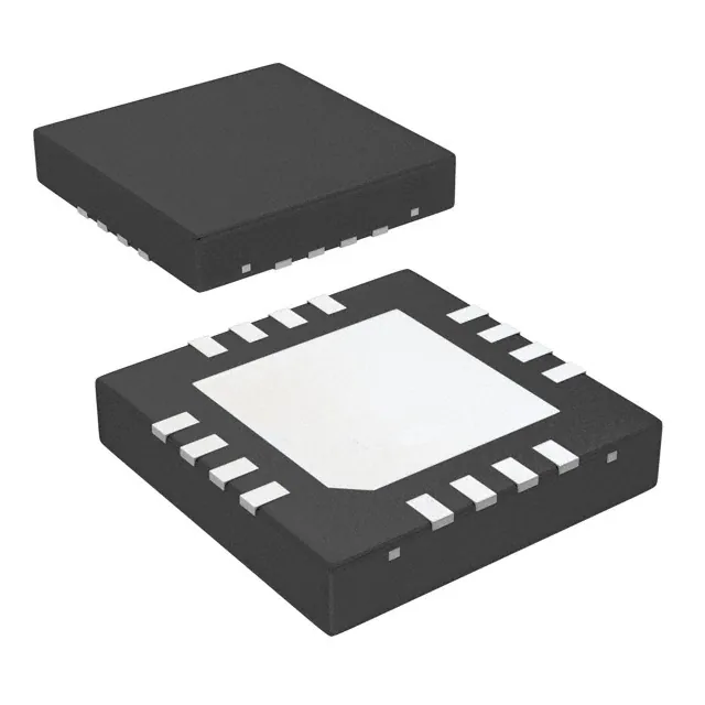


 工商网监
湘ICP备2023018690号
工商网监
湘ICP备2023018690号
