User's Guide
SLAU534 – September 2013
HD3SS213 Evaluation Module
This is the user’s guide for the evaluation module (EVM) of the HD3SS213. The purpose of this user’s
guide is to facilitate an easy evaluation process of the HD3SS213 DisplayPort switch.
The contents of this user’s guide are meant to provide an overview of the HD3SS213, which includes
highlighting its key features, operating conditions, and how to setup this EVM for use in a system level
evaluation.
The construction of the HD3SS213 EVM also serves as a reference design that can be easily modified for
any intended application. Target applications include Notebooks, Desktops and Docking Stations.
Schematic and layout information is included at the end of this manual.
1
2
3
4
5
6
7
8
Contents
Introduction .................................................................................................................. 2
HD3SS213 EVM Kit Contents ............................................................................................. 2
Description of EVM Board ................................................................................................. 2
Power for the HD3SS213 EVM ........................................................................................... 3
Monitoring the Device Current ............................................................................................ 3
PCB Construction ........................................................................................................... 3
6.1
HD3SS213 EVM Board Schematics ............................................................................. 3
6.2
HD3SS213 EVM Board Layout .................................................................................. 8
HD3SS213 EVM Board Construction .................................................................................... 9
HD3SS213 EVM Material Listing ........................................................................................ 10
List of Figures
1
HD3SS213 EVM Simple System Block Diagram .......................................................................
2
2
HD3SS213 EVM Picture [Top Side] ......................................................................................
3
3
HD3SS213 EVM Schematic Source Port C .............................................................................
4
4
HD3SS213 EVM Schematic Sink Ports A and B .......................................................................
5
5
HD3SS213 EVM Control ...................................................................................................
6
6
HD3SS213 EVM Power ....................................................................................................
7
7
HD3SS213 EVM Layout Layer 1 [Top]...................................................................................
8
8
HD3SS213 EVM Layout Layer 2 [GND] .................................................................................
8
9
HD3SS213 EVM Layout Layer 3 [VCC]..................................................................................
9
10
HD3SS213 EVM Layout Layer 4 [Bottom] ...............................................................................
9
1
HD3SS213 EVM Jumper Description and Settings ....................................................................
3
2
EVM Bill of Materials ......................................................................................................
10
List of Tables
SLAU534 – September 2013
Submit Documentation Feedback
HD3SS213 Evaluation Module
Copyright © 2013, Texas Instruments Incorporated
1
�Introduction
1
www.ti.com
Introduction
The HD3SS213 is a high-speed passive switch capable of switching two full DisplayPort 4 lane ports from
one of two sources to one target location in an application or one source to one of two targets. For
DisplayPort Applications the HD3SS213 also supports switching of the Auxiliary (AUX), Display Data
Channel (DDC) and Hot Plug Detect (HPD) signals.
This EVM was designed to be used as a medium connection between one DisplayPort source and one of
two DisplayPort sinks. The interface to the EVM consists of a standard DisplayPort connector to connect
the EVM to your system set up via standard DisplayPort cables. Your test setup should look similar to
Figure 1
DisplayPort Device/Sink 1
DisplayPort Device/Sink 2
DisplayPort
Cables
Port A Connector
Port B Connector
HD3SS213 EVM
Port C Connector
DisplayPort
Cable
DisplayPort Host/Source
Figure 1. HD3SS213 EVM Simple System Block Diagram
2
HD3SS213 EVM Kit Contents
This EVM kit should contain the following items:
• HD3SS213 EVM board
• 9V DC Power Supply
• This user’s manual
3
Description of EVM Board
The HD3SS213 EVM is designed to provide easy evaluation of the HD3SS213 device. It is also meant to
serve as a reference design to show a practical example of how to use the device in a mass-production
system. Table 1 highlights the EVM jumper functionality and configuration.
2
HD3SS213 Evaluation Module
SLAU534 – September 2013
Submit Documentation Feedback
Copyright © 2013, Texas Instruments Incorporated
�Power for the HD3SS213 EVM
www.ti.com
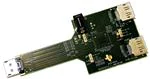
Figure 2. HD3SS213 EVM Picture [Top Side]
Table 1. HD3SS213 EVM Jumper Description and Settings
Jumper Configuration
4
JMP10
VDD Selection
No Connect for Nominal 3.3V Supply Voltage
Jumper pins 1-2 for 3.6V Supply Voltage
Jumper pins 2-3 for 3.0V Supply Voltage
JMP11
HD3SS213 Output Enable
Jumper pins 1-2 to enable device outputs (Default)
Jumper pins 2-3 to disable device outputs
JMP4
HD3SS213 AUX SEL
Jumper pins 1-2 to enable Port B to C Connection
Jumper pins 2-3 to enable Port A to C Connection
JMP13
HD3SS213 Dx SEL
Jumper pins 1-2 to enable Port B to C Connection
Jumper pins 2-3 to enable Port A to C Connection
Power for the HD3SS213 EVM
The HD3SS213 EVM kit comes with a +9V DC power supply that plugs into a wall socket.
5
Monitoring the Device Current
To observe current consumption of the HD3SS213 in the device evaluation, the HD3SS213 EVM includes
the option of monitoring the current draw of the device. In order to enable this feature, the following steps
must be taken:
1. Un-install the ferrite bead located at L2.
2. Obtain a power supply with the ability to display its current draw (or connect a current meter in series
to the power supply) and connect to JMP 9
Turn on the power supply and observe the measured current on the power supply display (or current
meter).
6
PCB Construction
This section discusses the construction of the EVM boards. It includes the board schematics and layout
files to show how the board was built.
6.1
HD3SS213 EVM Board Schematics
This section shows the board schematic sheets for the EVM.
SLAU534 – September 2013
Submit Documentation Feedback
HD3SS213 Evaluation Module
Copyright © 2013, Texas Instruments Incorporated
3
�PCB Construction
www.ti.com
Figure 3. HD3SS213 EVM Schematic Source Port C
4
HD3SS213 Evaluation Module
SLAU534 – September 2013
Submit Documentation Feedback
Copyright © 2013, Texas Instruments Incorporated
�PCB Construction
www.ti.com
Figure 4. HD3SS213 EVM Schematic Sink Ports A and B
SLAU534 – September 2013
Submit Documentation Feedback
HD3SS213 Evaluation Module
Copyright © 2013, Texas Instruments Incorporated
5
�PCB Construction
www.ti.com
Figure 5. HD3SS213 EVM Control
6
HD3SS213 Evaluation Module
SLAU534 – September 2013
Submit Documentation Feedback
Copyright © 2013, Texas Instruments Incorporated
�PCB Construction
www.ti.com
Figure 6. HD3SS213 EVM Power
SLAU534 – September 2013
Submit Documentation Feedback
HD3SS213 Evaluation Module
Copyright © 2013, Texas Instruments Incorporated
7
�PCB Construction
6.2
www.ti.com
HD3SS213 EVM Board Layout
This EVM was designed to show the implementation of this device on a 4-layer board.
Figure 7. HD3SS213 EVM Layout Layer 1 [Top]
Figure 8. HD3SS213 EVM Layout Layer 2 [GND]
8
HD3SS213 Evaluation Module
SLAU534 – September 2013
Submit Documentation Feedback
Copyright © 2013, Texas Instruments Incorporated
�HD3SS213 EVM Board Construction
www.ti.com
Figure 9. HD3SS213 EVM Layout Layer 3 [VCC]
Figure 10. HD3SS213 EVM Layout Layer 4 [Bottom]
7
HD3SS213 EVM Board Construction
The HD3SS213 EVM board is a 4-layer board constructed of FR4 – TurboClad 370 material. The board
stack-up consists of a signal layer on top, a ground layer, power layer, and a signal layer on bottom.
NOTE: Note: To achieve the desired impedance, it is recommended that you consult the board
manufacturer for their process and design requirements.
SLAU534 – September 2013
Submit Documentation Feedback
HD3SS213 Evaluation Module
Copyright © 2013, Texas Instruments Incorporated
9
�HD3SS213 EVM Material Listing
8
www.ti.com
HD3SS213 EVM Material Listing
Table 2. EVM Bill of Materials
10
Item
Quantity
Reference
Value
1
2
C20, C37
1.0uF
2
3
C65, C68, C69
0.1uF
3
3
C66, C70, C71
0.01uF
4
1
C67
1.0uF
5
2
C73, C74
1.0 uF
6
1
D3
GREEN
7
1
D4
10V, 3A
8
1
JMP4
4 Pin-T Berg Jumper
9
1
JMP9
DNI
10
1
JMP10
DNI
11
2
JMP11, JMP13
Header 3x1
12
1
J18
DP Plug Source
13
2
J21, J22
Display_Port_Connector_Source
14
1
L2
HI1206N101R-00
15
1
P1
RAPC722
16
1
R2
DNI 100k
17
5
R3, R14, R17, R33, R45
100K
18
28
R4, R6, R16, R18, R25, R27, R34, R35, R42, R43, R49,
R57, R58, R59, R60, R61, R62, R63, R64, R65, R66, R67, 0
R68, R69, R70, R71, R72, R73
19
3
R5 R20, R44
DNI 0
20
2
R7, R8
DNI 2K
21
1
R9
DNI 27K
22
1
R10
DNI 5M
23
2
R11, R46
1M
24
8
R22, R24, R28, R29, R30, R31, R47, R48
4.64K
25
4
R23, R36, R39, R74
DNI 0
26
1
R50
75
27
1
R51
23.2K
28
2
R52, R53
150K
29
1
R54
DNI
30
1
R55
64.9K
31
1
R56
13K
32
1
R75
0
33
1
R76
0
34
18
R111, R112, R113, R114, R115, R116, R117, R118,
R119, R120, R121, R122, R123, R124, R125, R126,
R129, R131
DNI 10K
35
2
R127, R128
DNI 1M
36
14
TP1, TP2, TP3, TP4, TP5, TP6, TP7, TP8, TP9, TP10,
TP11, TP12, TP13, TP14
Test Point
37
1
U4
REG104-A
38
1
U5
HD3SS213_ZQE
HD3SS213 Evaluation Module
SLAU534 – September 2013
Submit Documentation Feedback
Copyright © 2013, Texas Instruments Incorporated
�IMPORTANT NOTICE
Texas Instruments Incorporated and its subsidiaries (TI) reserve the right to make corrections, enhancements, improvements and other
changes to its semiconductor products and services per JESD46, latest issue, and to discontinue any product or service per JESD48, latest
issue. Buyers should obtain the latest relevant information before placing orders and should verify that such information is current and
complete. All semiconductor products (also referred to herein as “components”) are sold subject to TI’s terms and conditions of sale
supplied at the time of order acknowledgment.
TI warrants performance of its components to the specifications applicable at the time of sale, in accordance with the warranty in TI’s terms
and conditions of sale of semiconductor products. Testing and other quality control techniques are used to the extent TI deems necessary
to support this warranty. Except where mandated by applicable law, testing of all parameters of each component is not necessarily
performed.
TI assumes no liability for applications assistance or the design of Buyers’ products. Buyers are responsible for their products and
applications using TI components. To minimize the risks associated with Buyers’ products and applications, Buyers should provide
adequate design and operating safeguards.
TI does not warrant or represent that any license, either express or implied, is granted under any patent right, copyright, mask work right, or
other intellectual property right relating to any combination, machine, or process in which TI components or services are used. Information
published by TI regarding third-party products or services does not constitute a license to use such products or services or a warranty or
endorsement thereof. Use of such information may require a license from a third party under the patents or other intellectual property of the
third party, or a license from TI under the patents or other intellectual property of TI.
Reproduction of significant portions of TI information in TI data books or data sheets is permissible only if reproduction is without alteration
and is accompanied by all associated warranties, conditions, limitations, and notices. TI is not responsible or liable for such altered
documentation. Information of third parties may be subject to additional restrictions.
Resale of TI components or services with statements different from or beyond the parameters stated by TI for that component or service
voids all express and any implied warranties for the associated TI component or service and is an unfair and deceptive business practice.
TI is not responsible or liable for any such statements.
Buyer acknowledges and agrees that it is solely responsible for compliance with all legal, regulatory and safety-related requirements
concerning its products, and any use of TI components in its applications, notwithstanding any applications-related information or support
that may be provided by TI. Buyer represents and agrees that it has all the necessary expertise to create and implement safeguards which
anticipate dangerous consequences of failures, monitor failures and their consequences, lessen the likelihood of failures that might cause
harm and take appropriate remedial actions. Buyer will fully indemnify TI and its representatives against any damages arising out of the use
of any TI components in safety-critical applications.
In some cases, TI components may be promoted specifically to facilitate safety-related applications. With such components, TI’s goal is to
help enable customers to design and create their own end-product solutions that meet applicable functional safety standards and
requirements. Nonetheless, such components are subject to these terms.
No TI components are authorized for use in FDA Class III (or similar life-critical medical equipment) unless authorized officers of the parties
have executed a special agreement specifically governing such use.
Only those TI components which TI has specifically designated as military grade or “enhanced plastic” are designed and intended for use in
military/aerospace applications or environments. Buyer acknowledges and agrees that any military or aerospace use of TI components
which have not been so designated is solely at the Buyer's risk, and that Buyer is solely responsible for compliance with all legal and
regulatory requirements in connection with such use.
TI has specifically designated certain components as meeting ISO/TS16949 requirements, mainly for automotive use. In any case of use of
non-designated products, TI will not be responsible for any failure to meet ISO/TS16949.
Products
Applications
Audio
www.ti.com/audio
Automotive and Transportation
www.ti.com/automotive
Amplifiers
amplifier.ti.com
Communications and Telecom
www.ti.com/communications
Data Converters
dataconverter.ti.com
Computers and Peripherals
www.ti.com/computers
DLP® Products
www.dlp.com
Consumer Electronics
www.ti.com/consumer-apps
DSP
dsp.ti.com
Energy and Lighting
www.ti.com/energy
Clocks and Timers
www.ti.com/clocks
Industrial
www.ti.com/industrial
Interface
interface.ti.com
Medical
www.ti.com/medical
Logic
logic.ti.com
Security
www.ti.com/security
Power Mgmt
power.ti.com
Space, Avionics and Defense
www.ti.com/space-avionics-defense
Microcontrollers
microcontroller.ti.com
Video and Imaging
www.ti.com/video
RFID
www.ti-rfid.com
OMAP Applications Processors
www.ti.com/omap
TI E2E Community
e2e.ti.com
Wireless Connectivity
www.ti.com/wirelessconnectivity
Mailing Address: Texas Instruments, Post Office Box 655303, Dallas, Texas 75265
Copyright © 2013, Texas Instruments Incorporated
�