Product
Folder
Sample &
Buy
Support &
Community
Tools &
Software
Technical
Documents
HD3SS3411
SLASEB6 – NOVEMBER 2015
HD3SS3411 One Channel Differential 2:1 Mux/Demux
1 Features
3 Description
•
The HD3SS3411 is a high-speed bi-directional
passive switch in multiplexer or demultiplexer
configurations. Based on control pin SEL, the device
provides switching of differential channels between
Port B to Port A or Port C to Port A.
1
•
•
•
•
•
•
•
Compatible with Multiple Interface Standards
Including FPD Link, LVDS, PCIE Gen II, III, XAUI,
and USB3.1
Operates up to 10 Gbps
Wide –3 dB Differential BW of ~ 7.5 GHz
Excellent Dynamic Characteristics (at 4 GHz)
– Insertion Loss = -1.1 dB
– Return Loss = -11.3 dB
– Off Isolation = –19 dB
Bidirectional "Mux/De-Mux" Differential Switch
Supports Common Mode Voltage 0 V to 2 V
Single Supply Voltage VCC of 3.3 V ±10%
Industrial Temperature Range of -40°C to 105°C
The HD3SS3411 is a generic analog differential
passive switch that can work for any high speed
interface application as long as it is biased at a
common mode voltage range of 0 V to 2 V and has
differential signaling with differential amplitude up to
1800 mVpp. The device employs adaptive tracking
that ensures the channel remains unchanged for
entire common mode voltage range.
Excellent dynamic characteristics of the device allow
high speed switching with minimum attenuation to the
signal eye diagram with little added jitter. It consumes
< 2 mW of power when operational and has a
shutdown mode exercisable by OEn pin resulting
< 2 µW.
2 Applications
•
•
•
•
•
Industrial Data Switching
Desktop and Notebook PCs
Server/Storage Area Networks
PCI Express Backplanes
Shared I/O Ports
Device Information(1)
PART NUMBER
HD3SS3411
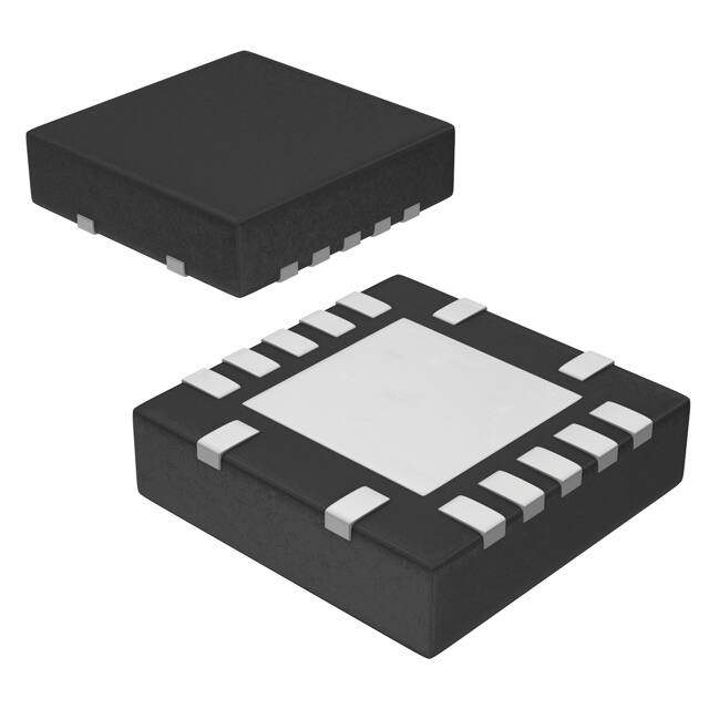
PACKAGE
WQFN (14)
HD3SS3411I
BODY SIZE (NOM)
3.50 mm x 3.50 mm
(1) For all available packages, see the orderable addendum at
the end of the data sheet.
Simplified Schematic
VCC
Bp
Bn
Ap
An
Cp
Cn
SEL
GND
1
An IMPORTANT NOTICE at the end of this data sheet addresses availability, warranty, changes, use in safety-critical applications,
intellectual property matters and other important disclaimers. PRODUCTION DATA.
�HD3SS3411
SLASEB6 – NOVEMBER 2015
www.ti.com
Table of Contents
1
2
3
4
5
6
7
Features ..................................................................
Applications ...........................................................
Description .............................................................
Revision History.....................................................
Pin Configuration and Functions .........................
Specifications.........................................................
1
1
1
2
3
4
6.1
6.2
6.3
6.4
6.5
6.6
6.7
4
4
4
4
5
5
6
Absolute Maximum Ratings ......................................
ESD Ratings..............................................................
Recommended Operating Conditions.......................
Thermal Information ..................................................
Electrical Characteristics...........................................
Timing Requirements ................................................
Typical Characteristics ..............................................
8
8.1
8.2
8.3
8.4
8.5
Overview ...................................................................
Functional Block Diagram .........................................
Feature Description...................................................
Device Functional Modes..........................................
Application Information.............................................. 9
Typical Application .................................................... 9
Design Requirements.............................................. 10
Detailed Design Procedure ..................................... 10
Application Curves .................................................. 12
9 Power Supply Recommendations...................... 12
10 Layout................................................................... 13
10.1 Layout Guidelines ................................................. 13
10.2 Layout Example .................................................... 14
11 Device and Documentation Support ................. 15
11.1
11.2
11.3
11.4
11.5
Detailed Description .............................................. 7
7.1
7.2
7.3
7.4
Application Information and Implementation ..... 9
7
7
7
8
Documentation Support .......................................
Community Resources..........................................
Trademarks ...........................................................
Electrostatic Discharge Caution ............................
Glossary ................................................................
15
15
15
15
15
12 Mechanical, Packaging, and Orderable
Information ........................................................... 15
4 Revision History
2
DATE
REVISION
NOTES
November 2015
*
Initial release.
Submit Documentation Feedback
Copyright © 2015, Texas Instruments Incorporated
Product Folder Links: HD3SS3411
�HD3SS3411
www.ti.com
SLASEB6 – NOVEMBER 2015
5 Pin Configuration and Functions
RWA Package
14 Pin (WQFN)
Top View
OEn
GND
1
14
Ap 2
13 Bp
An 3
12 Bn
VCC 4
11 GND
GND 5
10 Cp
RSVD 6
9
7
8
SEL
GND
Cn
Pin Functions
NAME
NO
TYPE
Ap
2
I/O
Port A, High Speed Positive Signal
DESCRIPTION
An
3
I/O
Port A, High Speed Negative Signal
Bp
13
I/O
Port B, High Speed Positive Signal
Bn
12
I/O
Port B, High Speed Negative Signal
Cp
10
I/O
Port C, High Speed Positive Signal
Cn
9
I/O
Port C, High Speed Negative Signal
GND
5,8,11,14,
Pad
G
Ground
OEn
1
I
Active Low Chip Enable
L: Normal operation
H: Shutdown
RSVD
6
I/O
SEL
7
I
Port select pin
L: Port A to Port B
H: Port A to Port C
VCC
4
P
3.3 V power
Reserved Pin – connect or pull-down to GND
Submit Documentation Feedback
Copyright © 2015, Texas Instruments Incorporated
Product Folder Links: HD3SS3411
3
�HD3SS3411
SLASEB6 – NOVEMBER 2015
www.ti.com
6 Specifications
6.1 Absolute Maximum Ratings (1)
Over operating free-air temperature range (unless otherwise noted)
Supply voltage range (VCC)
Voltage range
(1)
MIN
MAX
UNIT
Absolute minimum/maximum supply voltage range
–0.5
4
V
Differential I/O
–0.5
2.5
Control pin
–0.5
VDD + 0.5
V
Stresses beyond those listed under absolute maximum ratings may cause permanent damage to the device. These are stress ratings
only and functional operation of the device at these or any conditions beyond those indicated under recommended operating conditions
is not implied. Exposure to absolute-maximum-rated conditions for extended periods may affect device reliability.
6.2 ESD Ratings
VALUE
V(ESD)
(1)
Electrostatic discharge
Human-body model (HBM), per AEC Q100-002 (1)
±2000
Charged-device model (CDM), per AEC Q100-011
±500
UNIT
V
AEC Q100-002 indicates that HBM stressing shall be in accordance with the ANSI/ESDA/JEDEC JS-001 specification.
6.3 Recommended Operating Conditions
over operating free-air temperature range (unless otherwise noted)
MIN
VCC
Supply voltage
VIH
Input high voltage (SEL, OEn Pin)
VIL
Input low voltage (SEL OEn Pin)
VDiff
High speed signal pins differential voltage
VCM
Common mode voltage (differential pins)
TA
Operating free-air temperature
NOM
MAX
UNIT
3
3.6
V
V
2
VCC
–0.1
0.8
V
0
1.8
VPP
0
2
V
–40
105
°C
6.4 Thermal Information
HD3SS3411
THERMAL METRIC (1)
RWA (WQFN)
UNIT
14 PINS
RθJA
Junction-to-ambient thermal resistance
50.5
RθJC(top)
Junction-to-case (top) thermal resistance
63.1
RθJB
Junction-to-board thermal resistance
26.4
ψJT
Junction-to-top characterization parameter
2.2
ψJB
Junction-to-board characterization parameter
26.5
RθJC(bot)
Junction-to-case (bottom) thermal resistance
7.3
(1)
4
°C/W
For more information about traditional and new thermal metrics, see the IC Package Thermal Metrics application report, SPRA953.
Submit Documentation Feedback
Copyright © 2015, Texas Instruments Incorporated
Product Folder Links: HD3SS3411
�HD3SS3411
www.ti.com
SLASEB6 – NOVEMBER 2015
6.5 Electrical Characteristics
over operating free-air temperature range (unless otherwise noted)
PARAMETER
TEST CONDITIONS
MIN
TYP
MAX
UNITS
ICC
Device active Current
VCC = 3.3 V, OEn = 0
0.6
0.8
mA
ISTDN
Device shutdown Current
VCC = 3.3 V, OEn = 0
0.3
0.6
µA
CON
Outputs ON Capacitance
0.6
RON
Output ON resistance
VCC = 3.3 V; VCM = 0 V to 2 V ;
IO = –8 mA
ΔRON
On resistance match between pairs of
the same channel
VCC = 3.3 V ; –0.35 V ≤ VIN ≤ 2.35 V;
IO = –8 mA
R(FLAT_ON)
On resistance flatness
(RON(MAX) – RON(MAIN)
VDD = 3.3 V; –0.35 V ≤ VIN ≤ 2.35 V
IIH(CTRL)
IIL(CTRL)
pF
8
Ω
0.5
Ω
1
Ω
Input high current, control pins
(SEL, OEn)
1
µA
Input low current, control pins
(SEL, OEn)
1
µA
1
µA
140
µA
1
µA
5
[A/B/C][p/n] VIN = 2 V for selected port,
A and B with SEL= 0, and A and C with
SEL = VCC
IIH(HS)
IIL(HS)
Input high current, high speed pins
Input low current, high speed pins
[A/B/C][p/n] VIN = 2 V for non-selected
port, C with SEL= 0, and B with
SEL = VCC
(Note there is a 20 KΩ pull-down in nonselected port)
100
[A/B/C][p/n]
High Speed Performance
IL
BW
RL
Differential Insertion Loss
f = 0.3 MHz
–0.5
f = 2.5 GHz
–0.7
f = 4 GHz
–1.1
-3 dB Bandwidth
Differential return loss
OI
Differential OFF isolation
Xtalk
Differential Crosstalk
dB
7.5
f = 0.3 MHz
–26.4
f = 2.5 GHz
–16.6
f = 4 GHz
–11.3
f = 0.3 MHz
–75
f = 2.5 GHz
–22
f = 4 GHz
–19
f = 4 GHz
–35
GHz
dB
dB
dB
6.6 Timing Requirements
MIN
NOM
MAX
UNIT
tPD
Switch propagation delay
80
ps
tSW
Switching time
0.5
ns
tSK_INTRA
Intra-pair output skew
5
ps
Submit Documentation Feedback
Copyright © 2015, Texas Instruments Incorporated
Product Folder Links: HD3SS3411
5
�HD3SS3411
SLASEB6 – NOVEMBER 2015
www.ti.com
0
2
-5
0
Insertion Loss, S21 (dB)
Return Loss, S11 (dB)
6.7 Typical Characteristics
-10
-15
-20
-25
-2
-4
-6
-8
-10
-12
-30
0
2
4
6
Frequency (GHz)
8
10
0
D001
Figure 1. Return Loss vs Frequency
6
Submit Documentation Feedback
2
4
6
Frequency (GHz)
8
10
D002
Figure 2. Insertion Loss vs Frequency
Copyright © 2015, Texas Instruments Incorporated
Product Folder Links: HD3SS3411
�HD3SS3411
www.ti.com
SLASEB6 – NOVEMBER 2015
7 Detailed Description
7.1 Overview
The HD3SS3411 is a high-speed bi-directional passive switch in mux or demux configurations. Based on control
pin SEL, the device switches one differential channels between Port B or Port C to Port A.
The HD3SS3411 is a generic analog differential passive switch that can work for any high speed interface
applications as long as it is biased at a common mode voltage range of 0 V to 2 V and has differential signaling
with differential amplitude up to 1800 mVpp. The device employs an adaptive tracking that ensures the channel
remains unchanged for entire common mode voltage range.
Table 1. MUX Pin Connections (1)
PORT B OR PORT C CHANNEL CONNECTED TO PORT A
CHANNEL
PORT A CHANNEL
(1)
SEL = L
SEL = H
Ap
Bp
Cp
An
Bn
Cn
The HD3SS3411 can tolerate polarity inversions for all differential signals on Ports A, B and C. Care
should be taken to ensure the same polarity is maintained on Port A vs. Port B/C.
7.2 Functional Block Diagram
VCC
Bp
Bn
Ap
An
Cp
Cn
SEL
GND
7.3 Feature Description
7.3.1 Output Enable and Power Savings
The HD3SS3411 has two power modes, normal operating mode and shutdown mode. During shutdown mode,
the device consumes very-little current to save the maximum power. The OEn control pin is used to toggle
between the two modes.
HD3SS3411 consumes < 2 mW of power when operational and has a shutdown mode exercisable by the OEn
pin resulting < 20 µW.
Submit Documentation Feedback
Copyright © 2015, Texas Instruments Incorporated
Product Folder Links: HD3SS3411
7
�HD3SS3411
SLASEB6 – NOVEMBER 2015
www.ti.com
7.4 Device Functional Modes
The OEn control pin selects the functional mode of HD3SS3411. To enter standby/shutdown mode, the OEn
control pin is pulled high through a resistor and must remain high. For active/normal operation, the OEn control
pin should be pulled low to GND or dynamically controlled to switch between H or L.
Table 2. Device Power Modes
OEn
8
Device State
Signal Pins
L
Normal
Normal
H
Shutdown
Tri-stated
Submit Documentation Feedback
Copyright © 2015, Texas Instruments Incorporated
Product Folder Links: HD3SS3411
�HD3SS3411
www.ti.com
SLASEB6 – NOVEMBER 2015
8 Application Information and Implementation
NOTE
Information in the following applications sections is not part of the TI component
specification, and TI does not warrant its accuracy or completeness. TI’s customers are
responsible for determining suitability of components for their purposes. Customers should
validate and test their design implementation to confirm system functionality.
8.1 Application Information
HD3SS3411 mux channels have independent adaptive common mode tracking allowing RX and TX paths to
have different common mode voltage simplifying system implementation and avoiding inter-operational issues.
HD3SS3411 mux does not provide common mode biasing for the channel. Therefore, it is required that the
device is biased from either side for all active channels.
The HD3SS3411 supports several high-speed data protocols with a differential amplitude of < 1800 mVpp and a
common mode voltage of < 2 V, as with USB 3.1 and DisplayPort 1.3. The one select input (SEL) pin can be
controlled by an available GPIO pin within a system or from a microcontroller.
8.2 Typical Application
Serializer A
Camera A
FSYNC
I2C
HD3SS3411
Analog
MUX
Image
Sensor
VDD33
VDDIO
(3.3V) (1.8V or 3.3V)
DATA
PCLK
RIN+
RIN-
100 ohm STP Cable
PDB
OSS_SEL
OEN
MODE_SEL
INTB_IN
DATA
PCLK
Video
Source
R(7;0)
G(7;0)
B(7;0)
HS
VS
DE
PCLK
Deserializer
RGB Display
720p
24-bit color
depth
LOCK
PASS
I2S AUDIO
(STEREO)
MCLK
SCL
SDA
IDX
DAP
I2C
Serializer B
Figure 3. FPD Link III Application
Submit Documentation Feedback
Copyright © 2015, Texas Instruments Incorporated
Product Folder Links: HD3SS3411
9
�HD3SS3411
SLASEB6 – NOVEMBER 2015
www.ti.com
8.3 Design Requirements
For this design example, use the values shown in Table 3.
Table 3. Design Paramerters
PARAMETER
VALUE
VCC voltage
3.3 V
Ap/n, Bp/n, Cp/n CM input voltage
0 V to 2 V
SEL/OEn pin max voltage for low
0V
SEL/OEn pin min voltage for high
3.3 V
8.4 Detailed Design Procedure
8.4.1 AC Coupling Capacitors
Many interfaces require AC coupling between the transmitter and receiver. The 0402 capacitors are the preferred
option to provide AC coupling, and the 0603 size capacitors will also work. The 0805 size capacitors and Cpacks should be avoided. When placing AC coupling capacitors symmetric placement is best. A capacitor value
of 0.1 µF is best and the value should be match for the ± signal pair. The placement should be along the TX
pairs on the system board, which are usually routed on the top layer of the board.
HD3SS3411
HD3SS3411
There are several placement options for the AC coupling capacitors. Because the switch requires a bias voltage,
the capacitors must only be placed on one side of the switch. If they are placed on both sides of the switch, a
biasing voltage should be provided. A few placement options are shown below. In Figure 4, the coupling
capacitors are placed between the switch and endpoint. In this situation, the switch is biased by the system/host
controller.
Figure 4. AC Coupling Capacitors Between Switch TX and Endpoint TX
10
Submit Documentation Feedback
Copyright © 2015, Texas Instruments Incorporated
Product Folder Links: HD3SS3411
�HD3SS3411
www.ti.com
SLASEB6 – NOVEMBER 2015
Detailed Design Procedure (continued)
HD3SS3411
HD3SS3411
In Figure 5, the coupling capacitors are placed on the host transmit pair and endpoint transmit pair. In this
situation, the switch on the top is biased by the endpoint and the lower switch is biased by the host controller.
Figure 5. AC Coupling Capacitors on Host TX and Endpoint TX
HD3SS3411
HD3SS3411
If the common mode voltage in the system is higher than 2 V, the coupling capacitors are placed on both sides of
the switch (shown in Figure 6). A biasing voltage of less than 2 V is required in this case.
Figure 6. AC Coupling Capacitors on Both Sides of Switch
Submit Documentation Feedback
Copyright © 2015, Texas Instruments Incorporated
Product Folder Links: HD3SS3411
11
�HD3SS3411
SLASEB6 – NOVEMBER 2015
www.ti.com
8.5 Application Curves
Figure 7. 6 Gbps Source Eye Diagram
Figure 8. 6 Gbps Output Eye Diagram
9 Power Supply Recommendations
There is no power supply sequence required for HD3SS3411. However, it is recommended that OEn is asserted
low after device supply VCC is stable and in specifications. It is also recommended that ample decoupling
capacitors are placed at the device VCC near the pin.
12
Submit Documentation Feedback
Copyright © 2015, Texas Instruments Incorporated
Product Folder Links: HD3SS3411
�HD3SS3411
www.ti.com
SLASEB6 – NOVEMBER 2015
10 Layout
10.1 Layout Guidelines
10.1.1 Critical Routes
• The high speed differential signals must be routed with great care to minimize signal quality degradation
between the connector and the source or sink of the high speed signals by following the guidelines provided
in this document. Depending on the configuration schemes, the speed of each differential pair can reach a
maximum speed of 10 Gbps. These signals are to be routed first before other signals with highest priority.
• Each differential pair should be routed together with controlled differential impedance of 85-Ω to 90-Ω and 50Ω common mode impedance. Keep away from other high speed signals. The number of vias should be kept
to minimum. Each pair should be separated from adjacent pairs by at least 3 times the signal trace width.
Route all differential pairs on the same group of layers (Outer layers or inner layers) if not on the same layer.
No 90 degree turns on any of the differential pairs. If bends are used on high speed differential pairs, the
angle of the bend should be greater than 135 degrees.
• Length matching:
– Keep high speed differential pairs lengths within 5 mil of each other to keep the intra-pair skew minimum.
The inter-pair matching of the differential pairs is not as critical as intra-pair matching.
• Keep high speed differential pair traces adjacent to ground plane.
• Do not route differential pairs over any plane split.
• ESD components on the high speed differential lanes should be placed nearest to the connector in a pass
through manner without stubs on the differential path.
• For ease of routing, the P and N connection of the USB3.1 differential pairs to the HD3SS3411 pins can be
swapped.
10.1.2 General Routing/Placement Rules
• Follow 20H rule (H is the distance to ref-plane) for separation of the high speed trace from the edge of the
plane.
• Minimize parallelism of high speed clocks and other periodic signal traces to high speed lines.
• All differential pairs should be routed on the top or bottom layer (microstrip traces) if possible or on the same
group of layers. Vias should only be used in the breakout region of the device to route from the top to bottom
layer when necessary. Avoid using vias in the main region of the board at all cost. Use a ground reference via
next to signal via. Distance between ground reference via and signal need to be calculated to have similar
impedance as traces.
• All differential signals should not be routed over plane split. Changing signal layers is preferable to crossing
plane splits.
• Use of and proper placement of stitching caps when split plane crossing is unavoidable to account for high
frequency return current path.
• Route differential traces over a continuous plane with no interruptions.
• Do not route differential traces under power connectors or other interface connectors, crystals, oscillators, or
any magnetic source.
• Route traces away from etching areas like pads, vias, and other signal traces. Try to maintain a 20 mil keep
out distance where possible.
• Decoupling caps should be placed next to each power terminal on the HD3SS3411. Care should be taken to
minimize the stub length of the trace connecting the capacitor to the power pin.
• Avoid sharing vias between multiple decoupling caps.
• Place vias as close as possible to the decoupling cap solder pad.
• Widen VCC/GND planes to reduce effect of static and dynamic IR drop.
Submit Documentation Feedback
Copyright © 2015, Texas Instruments Incorporated
Product Folder Links: HD3SS3411
13
�HD3SS3411
SLASEB6 – NOVEMBER 2015
www.ti.com
VCC
10.2 Layout Example
OEn and SEL can be controlled
by µC. OEn can also be tied
to Vcc with resistor
100nF
An
100nF
Place VCC decoupling caps as
close to VCC pins as possible
xxxx
xxxx
xxxx
xxxx
GND
Match High Speed traces
length as close as possible to
minimize Skew
1
Ap
OEn
10kQ
Match High Speed traces
length as close as possible to
minimize Skew
VCC
Bp
Bn
GND
GND
Cn
GND
SEL
GND
10kQ
RSVD
Cp
Figure 9. Layout
14
Submit Documentation Feedback
Copyright © 2015, Texas Instruments Incorporated
Product Folder Links: HD3SS3411
�HD3SS3411
www.ti.com
SLASEB6 – NOVEMBER 2015
11 Device and Documentation Support
11.1 Documentation Support
11.2 Community Resources
The following links connect to TI community resources. Linked contents are provided "AS IS" by the respective
contributors. They do not constitute TI specifications and do not necessarily reflect TI's views; see TI's Terms of
Use.
TI E2E™ Online Community TI's Engineer-to-Engineer (E2E) Community. Created to foster collaboration
among engineers. At e2e.ti.com, you can ask questions, share knowledge, explore ideas and help
solve problems with fellow engineers.
Design Support TI's Design Support Quickly find helpful E2E forums along with design support tools and
contact information for technical support.
11.3 Trademarks
E2E is a trademark of Texas Instruments.
All other trademarks are the property of their respective owners.
11.4 Electrostatic Discharge Caution
These devices have limited built-in ESD protection. The leads should be shorted together or the device placed in conductive foam
during storage or handling to prevent electrostatic damage to the MOS gates.
11.5 Glossary
SLYZ022 — TI Glossary.
This glossary lists and explains terms, acronyms, and definitions.
12 Mechanical, Packaging, and Orderable Information
The following pages include mechanical, packaging, and orderable information. This information is the most
current data available for the designated devices. This data is subject to change without notice and revision of
this document. For browser-based versions of this data sheet, refer to the left-hand navigation.
Submit Documentation Feedback
Copyright © 2015, Texas Instruments Incorporated
Product Folder Links: HD3SS3411
15
�PACKAGE OUTLINE
RWA0014A
WQFN - 0.8 mm max height
SCALE 3.200
PLASTIC QUAD FLATPACK - NO LEAD
3.65
3.35
A
B
PIN 1 INDEX AREA
EA
SE
D
3.65
3.35
C
0.8 MAX
SEATING PLANE
0.05
0.00
EL
0.08
2.05 0.1
2X 1.5
T
N
2X
2
9
O
6
(0.2) TYP
8
R
7
8X 0.5
2
PIN 1 ID
(OPTIONAL)
13
1
14
14X
0.5
0.3
14X
0.30
0.18
0.1
0.05
C A
B
4221612/B 01/2015
NOTES:
1. All linear dimensions are in millimeters. Any dimensions in parenthesis are for reference only. Dimensioning and tolerancing
per ASME Y14.5M.
2. This drawing is subject to change without notice.
3. The package thermal pad must be soldered to the printed circuit board for thermal and mechanical performance.
www.ti.com
�EXAMPLE BOARD LAYOUT
RWA0014A
WQFN - 0.8 mm max height
PLASTIC QUAD FLATPACK - NO LEAD
(
2.05)
2X (1.5)
SYMM
1
14
14X (0.6)
13
2
14X (0.25)
EA
SE
D
SYMM
(3.3)
(0.78)
8X (0.5)
9
6
EL
( 0.2) VIA
TYP
7
(R0.05) TYP
(0.78)
8
R
(3.3)
LAND PATTERN EXAMPLE
O
T
SCALE:20X
N
0.07 MAX
ALL AROUND
0.07 MIN
ALL SIDES
SOLDER MASK
OPENING
METAL
METAL UNDER
SOLDER MASK
SOLDER MASK
OPENING
NON SOLDER MASK
DEFINED
(PREFERRED)
SOLDER MASK
DEFINED
SOLDER MASK DETAILS
4221612/B 01/2015
NOTES: (continued)
4. This package is designed to be soldered to a thermal pad on the board. For more information, see Texas Instruments literature
number SLUA271 (www.ti.com/lit/slua271).
www.ti.com
�EXAMPLE STENCIL DESIGN
RWA0014A
WQFN - 0.8 mm max height
PLASTIC QUAD FLATPACK - NO LEAD
2X (1.5)
4X ( 0.92)
1
14
14X (0.6)
13
EA
SE
D
2
14X (0.25)
SYMM
(3.3)
(0.55)
8X (0.5)
9
EL
6
METAL
TYP
N
O
T
(R0.05) TYP
R
7
SYMM
8
(0.55)
(3.3)
SOLDER PASTE EXAMPLE
BASED ON 0.125 mm THICK STENCIL
EXPOSED PAD
80% PRINTED SOLDER COVERAGE BY AREA
SCALE:20X
4221612/B 01/2015
NOTES: (continued)
5. Laser cutting apertures with trapezoidal walls and rounded corners may offer better paste release. IPC-7525 may have alternate
design recommendations.
www.ti.com
�PACKAGE OPTION ADDENDUM
www.ti.com
10-Dec-2020
PACKAGING INFORMATION
Orderable Device
Status
(1)
Package Type Package Pins Package
Drawing
Qty
Eco Plan
(2)
Lead finish/
Ball material
MSL Peak Temp
Op Temp (°C)
Device Marking
(3)
(4/5)
(6)
HD3SS3411IRWAR
ACTIVE
WQFN
RWA
14
3000
RoHS & Green
NIPDAU
Level-2-260C-1 YEAR
-40 to 105
3411I
HD3SS3411IRWAT
ACTIVE
WQFN
RWA
14
250
RoHS & Green
NIPDAU
Level-2-260C-1 YEAR
-40 to 105
3411I
(1)
The marketing status values are defined as follows:
ACTIVE: Product device recommended for new designs.
LIFEBUY: TI has announced that the device will be discontinued, and a lifetime-buy period is in effect.
NRND: Not recommended for new designs. Device is in production to support existing customers, but TI does not recommend using this part in a new design.
PREVIEW: Device has been announced but is not in production. Samples may or may not be available.
OBSOLETE: TI has discontinued the production of the device.
(2)
RoHS: TI defines "RoHS" to mean semiconductor products that are compliant with the current EU RoHS requirements for all 10 RoHS substances, including the requirement that RoHS substance
do not exceed 0.1% by weight in homogeneous materials. Where designed to be soldered at high temperatures, "RoHS" products are suitable for use in specified lead-free processes. TI may
reference these types of products as "Pb-Free".
RoHS Exempt: TI defines "RoHS Exempt" to mean products that contain lead but are compliant with EU RoHS pursuant to a specific EU RoHS exemption.
Green: TI defines "Green" to mean the content of Chlorine (Cl) and Bromine (Br) based flame retardants meet JS709B low halogen requirements of


 工商网监
湘ICP备2023018690号
工商网监
湘ICP备2023018690号
