INA1
®
INA111
11
INA1
11
High Speed FET-Input
INSTRUMENTATION AMPLIFIER
FEATURES
DESCRIPTION
● FET INPUT: IB = 20pA max
The INA111 is a high speed, FET-input instrumentation amplifier offering excellent performance.
● LOW OFFSET VOLTAGE: 500µV max
● LOW OFFSET VOLTAGE DRIFT:
5µV/°C max
The INA111 uses a current-feedback topology providing extended bandwidth (2MHz at G = 10) and fast
settling time (4µs to 0.01% at G = 100). A single
external resistor sets any gain from 1 to over 1000.
● HIGH SPEED: TS = 4µs (G = 100, 0.01%)
● HIGH COMMON-MODE REJECTION:
106dB min
Offset voltage and drift are laser trimmed for excellent
DC accuracy. The INA111’s FET inputs reduce input
bias current to under 20pA, simplifying input filtering
and limiting circuitry.
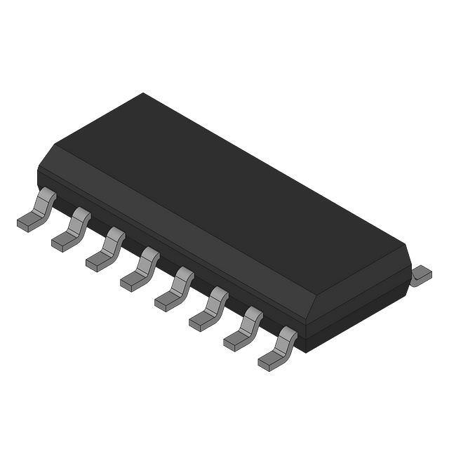
● 8-PIN PLASTIC DIP, SOL-16 SOIC
The INA111 is available in 8-pin plastic DIP, and
SOL-16 surface-mount packages, specified for the
–40°C to +85°C temperature range.
APPLICATIONS
● MEDICAL INSTRUMENTATION
● DATA ACQUISITION
V+
7 (13)
INA111
–
VIN
2
(4)
Feedback
A1
10kΩ
1
10kΩ
A3
RG
8
VIN
6
(11)
VO
G=1+
25kΩ
(15)
3
DIP Connected
Internally
25kΩ
(2)
+
(12)
5
A2
10kΩ
(5)
10kΩ
(10)
50kΩ
RG
Ref
4 (7)
DIP
(SOIC)
V–
International Airport Industrial Park • Mailing Address: PO Box 11400, Tucson, AZ 85734 • Street Address: 6730 S. Tucson Blvd., Tucson, AZ 85706 • Tel: (520) 746-1111 • Twx: 910-952-1111
Internet: http://www.burr-brown.com/ • FAXLine: (800) 548-6133 (US/Canada Only) • Cable: BBRCORP • Telex: 066-6491 • FAX: (520) 889-1510 • Immediate Product Info: (800) 548-6132
®
©
SBOS015
1992 Burr-Brown Corporation
PDS-1143E
1
INA111
Printed in U.S.A. March, 1998
�SPECIFICATIONS
ELECTRICAL
At TA = +25°C, VS = ±15V, RL = 2kΩ, unless otherwise noted.
INA111BP, BU
PARAMETER
CONDITIONS
INPUT
Offset Voltage, RTI
Initial
TA = +25°C
vs Temperature
TA = TMIN to TMAX
vs Power Supply
VS = ±6V to ±18V
Impedance, Differential
Common-Mode
Input Common-Mode Range
VDIFF = 0V
Common-Mode Rejection
VCM = ±10V, ∆RS = 1kΩ
G=1
G = 10
G = 100
G = 1000
TYP
MAX
±500 ± 2000/G
±5 ± 100/G
30 + 100/G
±10
±100 ± 500/G
±2 ± 10/G
2 +10/G
1012 || 6
1012 || 3
±12
80
96
106
106
90
110
115
115
BIAS CURRENT
OFFSET CURRENT
MIN
TYP
MAX
UNITS
±1000 ± 5000/G
±10 ± 100/G
✻
✻
±200 ± 500/G
±2 ± 20/G
✻
✻
✻
✻
µV
µV/°C
µV/V
Ω || pF
Ω || pF
V
75
90
100
100
✻
✻
✻
✻
±2
±20
✻
✻
pA
±0.1
±10
✻
✻
pA
13
10
10
1
✻
✻
✻
✻
nV/√Hz
nV/√Hz
nV/√Hz
µVp-p
0.8
✻
fA/√Hz
✻
1 + (50kΩ/RG)
1
Gain vs Temperature
50kΩ Resistance(1)
G = 1, RL = 10kΩ
G = 10, RL = 10kΩ
G = 100, RL = 10kΩ
G = 1000, RL = 10kΩ
G=1
±0.01
±0.1
±0.15
±0.25
±1
±25
10000
±0.02
±0.5
±0.5
±1
±10
±100
G=1
G = 10
G = 100
G = 1000
±0.0005
±0.001
±0.001
±0.005
±0.005
±0.005
±0.005
±0.02
Nonlinearity
OUTPUT
Voltage
Load Capacitance Stability
Short Circuit Current
FREQUENCY RESPONSE
Bandwidth, –3dB
IO = 5mA, TMIN to TMAX
Overload Recovery
G=1
G = 10
G = 100
G = 1000
VO = ±10V, G = 2 to 100
G=1
G = 10
G = 100
G = 1000
50% Overdrive
POWER SUPPLY
Voltage Range
Current
VIN = 0V
Slew Rate
Settling Time, 0.01%
dB
dB
dB
dB
G = 1000, RS = 0Ω
NOISE VOLTAGE, RTI
f = 100Hz
f = 1kHz
f = 10kHz
fB = 0.1Hz to 10Hz
Noise Current
f = 10kHz
GAIN
Gain Equation
Range of Gain
Gain Error
INA111AP, AU
MIN
±11
✻
2
2
450
50
17
2
2
4
30
1
±6
TEMPERATURE RANGE
Specification
Operating
θJA
±12.7
1000
+30/–25
✻
±15
±3.3
–40
–40
±18
±4.5
✻
85
125
✻
✻
✻
✻
✻
✻
✻
✻
✻
0.05
✻
±0.7
±2
✻
✻
✻
✻
✻
✻
✻
±0.01
±0.01
±0.04
%
%
%
%
of
of
of
of
FSR
FSR
FSR
FSR
✻
✻
✻
V
pF
mA
✻
✻
✻
✻
✻
✻
✻
✻
✻
✻
MHz
MHz
kHz
kHz
V/µs
µs
µs
µs
µs
µs
✻
✻
✻
100
V/V
V/V
%
%
%
%
ppm/°C
ppm/°C
✻
✻
V
mA
✻
✻
°C
°C
°C/W
✻ Specification same as INA111BP.
NOTE: (1) Temperature coefficient of the “50kΩ” term in the gain equation.
The information provided herein is believed to be reliable; however, BURR-BROWN assumes no responsibility for inaccuracies or omissions. BURR-BROWN assumes
no responsibility for the use of this information, and all use of such information shall be entirely at the user’s own risk. Prices and specifications are subject to change
without notice. No patent rights or licenses to any of the circuits described herein are implied or granted to any third party. BURR-BROWN does not authorize or warrant
any BURR-BROWN product for use in life support devices and/or systems.
®
INA111
2
�ELECTROSTATIC
DISCHARGE SENSITIVITY
PIN CONFIGURATIONS
Top View
DIP
RG
1
8
RG
V–IN
2
7
V+
+
IN
3
6
VO
V–
4
5
Ref
V
Top View
This integrated circuit can be damaged by ESD. Burr-Brown
recommends that all integrated circuits be handled with appropriate precautions. Failure to observe proper handling and
installation procedures can cause damage.
ESD damage can range from subtle performance degradation
to complete device failure. Precision integrated circuits may
be more susceptible to damage because very small parametric
changes could cause the device not to meet its published
specifications.
SOL-16 Surface Mount
NC
1
16 NC
RG
2
15 RG
NC
3
14 NC
V–IN
4
13 V+
V+IN
5
12 Feedback
NC
6
11 VO
V–
7
10 Ref
NC
8
9
ORDERING INFORMATION
PRODUCT
PACKAGE
INA111AP
INA111BP
INA111AU
INA111BU
8-Pin Plastic DIP
8-Pin Plastic DIP
SOL-16 Surface-Mount
SOL-16 Surface-Mount
TEMPERATURE RANGE
–40°C
–40°C
–40°C
–40°C
to
to
to
to
+85°C
+85°C
+85°C
+85°C
PACKAGE INFORMATION
NC
PRODUCT
INA111AP
INA111BP
INA111AU
INA111BU
ABSOLUTE MAXIMUM RATINGS(1)
PACKAGE
8-Pin Plastic
8-Pin Plastic
16-Pin Surface
16-Pin Surface
PACKAGE DRAWING
NUMBER(1)
DIP
DIP
Mount
Mount
006
006
211
211
NOTE: (1) For detailed drawing and dimension table, please see end of data
sheet, or Appendix C of Burr-Brown IC Data Book.
Supply Voltage .................................................................................. ±18V
Input Voltage Range .......................................... (V–) –0.7V to (V+) +15V
Output Short-Circuit (to ground) .............................................. Continuous
Operating Temperature ................................................. –40°C to +125°C
Storage Temperature ..................................................... –40°C to +125°C
Junction Temperature .................................................................... +150°C
Lead Temperature (soldering, 10s) ............................................... +300°C
NOTE: Stresses above these ratings may cause permanent damage.
®
3
INA111
�TYPICAL PERFORMANCE CURVES
At TA = +25°C, VS = ±15V, unless otherwise noted.
GAIN vs FREQUENCY
COMMON-MODE REJECTION vs FREQUENCY
10k
120
Common-Mode Rejection (dB)
G = 1k
Gain (V/V)
1k
G = 100
100
G = 10
10
G=1
1
100
80
G = 1k
60
G = 100
40
G = 10
20
G=1
0
0.1
1k
10k
100k
1M
10
10M
100
1k
INPUT COMMON-MODE VOLTAGE RANGE
vs OUTPUT VOLTAGE
1M
120
y A1
ed b
Limit ut Swing
tp
+ Ou
VD/2
10
5
–
VO
+
–
VD/2
0
Limit
+ Ou ed by A
tput
Swin2
g
Power Supply Rejection (dB)
Common-Mode Voltage (V)
100k
POWER SUPPLY REJECTION vs FREQUENCY
15
+
VCM
(Any Gain)
A3 – Output
Swing Limit
–5
A3 + Output
Swing Limit
Lim
it
– O ed by
utpu
A
t Sw 2
ing
–10
–15
–15
by A 1 g
in
ited
Lim put Sw
t
u
O
–
100
80
G = 1k
60
G = 100
40
G = 10
G=1
20
0
–10
–5
0
5
10
10
15
100
1k
10k
100k
1M
Frequency (Hz)
Output Voltage (V)
INPUT-REFERRED NOISE VOLTAGE vs FREQUENCY
SETTLING TIME vs GAIN
1k
100
100
G=1
G = 10
G = 100, 1k
10
Settling Time (µs)
Input-Referred Noise Voltage (nV/√Hz)
10k
Frequency (Hz)
Frequency (Hz)
0.01%
10
0.1%
1
1
1
10
100
1k
10k
1
®
INA111
10
100
Gain (V/V)
Frequency (Hz)
4
1000
�TYPICAL PERFORMANCE CURVES (CONT)
At TA = +25°C, VS = ±15V, unless otherwise noted.
INPUT BIAS CURRENT vs TEMPERATURE
50
200
25
100
0
0
G ≥ 10
–100
–25
G=1
–200
–50
10n
0
1
–10m
2
3
4
–75
–25
0
25
50
75
100
Temperature (°C)
INPUT BIAS CURRENT
vs DIFFERENTIAL INPUT VOLTAGE
INPUT BIAS CURRENT
vs COMMON-MODE INPUT VOLTAGE
125
–10m
–15.7V
Input Bias Current (A)
–10µ
G = 10 G = 100
G = 1k
+1p
G=1
G = 10
+10p
G = 1k
–5
0
–100µ
–10µ
+1p
+15.7V
+15.7V
–10
–1m
G = 100
+100p
5
10
15
+10p
20
–20
–15
Differential Overload Voltage (V)
NOTE: One input grounded.
–10
–5
0
5
10
15
20
Common-Mode Voltage (V)
OUTPUT CURRENT LIMIT vs TEMPERATURE
MAXIMUM OUTPUT VOLTAGE SWING vs FREQUENCY
50
30
25
Short-Circuit Current (mA)
Peak-to-Peak Amplitude (V)
Input Bias Current (A)
–50
Time From Power Supply Turn-On (Minutes)
–100µ
–15
1p
0.01p
–1m
–20
10p
5
–15.7V
G=1
IOS
100p
0.1p
–300
–75
Ib
1n
Input Bias Current (A)
300
Referred-to-Input VOS Change (µV)
Referred-to-Input VOS Change (µV)
OFFSET VOLTAGE WARM-UP vs TIME
75
20
15
10
5
0
40
30
+ICL
–ICL
20
10
0
1k
10k
100k
1M
–75
10M
–50
–25
0
25
50
75
100
125
Temperature (°C)
Frequency (Hz)
®
5
INA111
�TYPICAL PERFORMANCE CURVES (CONT)
At TA = +25°C, VS = ±15V, unless otherwise noted.
TOTAL HARMONIC DISTORTION + NOISE
vs FREQUENCY
QUIESCENT CURRENT vs TEMPERATURE
1
3.5
3.4
G = 1k
0.1
THD + N (%)
Quiescent Current (mA)
VO = 3Vrms, RL = 2kΩ
Measurement BW = 80kHz
3.3
3.2
Single-Ended Drive G = 1
G = 100
0.01
G = 10
0.001
Differential Drive G = 1
3.1
0.0001
3.0
–75
–50
–25
0
25
50
75
100
20
125
100
1k
10k 20k
Frequency (Hz)
Temperature (°C)
LARGE SIGNAL RESPONSE, G = 100
SMALL SIGNAL RESPONSE, G = 1
+10
+0.1
0
0
–0.1
–10
0
10
0
20
10
Time (µs)
Time (µs)
LARGE SIGNAL RESPONSE, G = 100
SMALL SIGNAL RESPONSE, G = 1
+10
+0.1
0
0
–10
–0.1
0
10
20
0
Time (µs)
®
INA111
10
Time (µs)
6
20
20
�APPLICATION INFORMATION
The 50kΩ term in equation 1 comes from the sum of the two
internal feedback resistors. These are on-chip metal film
resistors which are laser trimmed to accurate absolute values. The accuracy and temperature coefficient of these
resistors are included in the gain accuracy and drift specifications of the INA111.
Figure 1 shows the basic connections required for operation
of the INA111. Applications with noisy or high impedance
power supplies may require decoupling capacitors close to
the device pins as shown.
The output is referred to the output reference (Ref) terminal
which is normally grounded. This must be a low-impedance
connection to assure good common-mode rejection. A resistance of 2Ω in series with the Ref pin will cause a typical
device with 90dB CMR to degrade to approximately 80dB
CMR (G = 1).
The stability and temperature drift of the external gain
setting resistor, RG, also affects gain. RG’s contribution to
gain accuracy and drift can be directly inferred from the gain
equation (1). Low resistor values required for high gain can
make wiring resistance important. Sockets add to the wiring
resistance, which will contribute additional gain error (possibly an unstable gain error) in gains of approximately 100
or greater.
SETTING THE GAIN
Gain of the INA111 is set by connecting a single external
resistor, RG:
G = 1 + 5 0kΩ
RG
DYNAMIC PERFORMANCE
The typical performance curve “Gain vs Frequency” shows
that the INA111 achieves wide bandwidth over a wide range
of gain. This is due to the current-feedback topology of the
INA111. Settling time also remains excellent over wide
gains.
(1)
Commonly used gains and resistor values are shown in
Figure 1.
V+
0.1µF
Pin numbers are
for DIP package.
–
VIN
7
INA111
2
A1
10kΩ
1
+
–
)
VO = G • (VIN – VIN
10kΩ
50kΩ
G=1+
RG
25kΩ
6
A3
RG
+
8
25kΩ
Load
VO
–
+
VIN
3
5
A2
10kΩ
4
DESIRED
GAIN
1
2
5
10
20
50
100
200
500
1000
2000
5000
10000
RG
(Ω)
NEAREST 1% RG
(Ω)
No Connection
50.00k
12.50k
5.556k
2.632k
1.02k
505.1
251.3
100.2
50.05
25.01
10.00
5.001
No Connection
49.9k
12.4k
5.62k
2.61k
1.02k
511
249
100
49.9
24.9
10
4.99
Ref
10kΩ
0.1µF
Also drawn in simplified form:
V–
–
VIN
RG
+
VIN
INA111
VO
Ref
FIGURE 1. Basic Connections
®
7
INA111
�INPUT BIAS CURRENT RETURN PATH
The INA111 exhibits approximately 6dB rise in gain at
2MHz in unity gain. This is a result of its current-feedback
topology and is not an indication of instability. Unlike an op
amp with poor phase margin, the rise in response is a
predictable +6dB/octave due to a response zero. A simple
pole at 700kHz or lower will produce a flat passband
response (see Input Filtering).
The input impedance of the INA111 is extremely high—
approximately 1012Ω. However, a path must be provided for
the input bias current of both inputs. This input bias current
is typically less than 10pA. High input impedance means
that this input bias current changes very little with varying
input voltage.
The INA111 provides excellent rejection of high frequency
common-mode signals. The typical performance curve,
“Common-Mode Rejection vs Frequency” shows this behavior. If the inputs are not properly balanced, however,
common-mode signals can be converted to differential sig–
+
nals. Run the VIN and VIN connections directly adjacent each
other, from the source signal all the way to the input pins. If
possible use a ground plane under both input traces. Avoid
running other potentially noisy lines near the inputs.
Input circuitry must provide a path for this input bias current
if the INA111 is to operate properly. Figure 3 shows various
provisions for an input bias current path. Without a bias
current return path, the inputs will float to a potential which
exceeds the common-mode range of the INA111 and the
input amplifiers will saturate.
If the differential source resistance is low, the bias current
return path can be connected to one input (see the thermocouple example in Figure 3). With higher source impedance,
using two resistors provides a balanced input with possible
advantages of lower input offset voltage due to bias current
and better high-frequency common-mode rejection.
NOISE AND ACCURACY PERFORMANCE
The INA111’s FET input circuitry provides low input bias
current and high speed. It achieves lower noise and higher
accuracy with high impedance sources. With source impedances of 2kΩ to 50kΩ the INA114 may provide lower offset
voltage and drift. For very low source impedance (≤1kΩ),
the INA103 may provide improved accuracy and lower
noise.
Crystal or
Ceramic
Transducer
OFFSET TRIMMING
INA111
1MΩ
The INA111 is laser trimmed for low offset voltage and
drift. Most applications require no external offset adjustment. Figure 2 shows an optional circuit for trimming the
output offset voltage. The voltage applied to Ref terminal is
summed at the output. Low impedance must be maintained
at this node to assure good common-mode rejection. The op
amp shown maintains low output impedance at high frequency. Trim circuits with higher source impedance should
be buffered with an op amp follower circuit to assure low
impedance on the Ref pin.
1MΩ
Thermocouple
INA111
10kΩ
INA111
–
VIN
V+
VO
RG
INA111
+
VIN
100µA
1/2 REF200
Ref
OPA177
±10mV
Adjustment Range
Center-tap provides
bias current return.
100Ω(1)
10kΩ
FIGURE 3. Providing an Input Common-Mode Current Path.
(1)
INPUT COMMON-MODE RANGE
100Ω(1)
The linear common-mode range of the input op amps of the
INA111 is approximately ±12V (or 3V from the power
supplies). As the output voltage increases, however, the
linear input range will be limited by the output voltage swing
of the input amplifiers, A1 and A2. The common-mode range
is related to the output voltage of the complete amplifier—
see performance curve “Input Common-Mode Range vs
Output Voltage”.
100µA
1/2 REF200
NOTE: (1) For wider trim range required
in high gains, scale resistor values larger
V–
FIGURE 2. Optional Trimming of Output Offset Voltage.
®
INA111
8
�the 1N4148 may have leakage currents far greater than the
input bias current of the INA111 and are usually sensitive to
light.
A combination of common-mode and differential input
voltage can cause the output of A1 or A2 to saturate. Figure
4 shows the output voltage swing of A1 and A2 expressed in
terms of a common-mode and differential input voltages.
For applications where input common-mode range must be
maximized, limit the output voltage swing by connecting the
INA111 in a lower gain (see performance curve “Input
Common-Mode Voltage Range vs Output Voltage”). If
necessary, add gain after the INA111 to increase the voltage
swing.
INPUT FILTERING
The INA111’s FET input allows use of an R/C input filter
without creating large offsets due to input bias current.
Figure 6 shows proper implementation of this input filter to
preserve the INA111’s excellent high frequency commonmode rejection. Mismatch of the common-mode input capacitance (C1 and C2), either from stray capacitance or
Input-overload often produces an output voltage that appears
normal. For example, consider an input voltage of +14V on
one input and +15V on the other input will obviously exceed
the linear common-mode range of both input amplifiers.
Since both input amplifiers are saturated to the nearly the
same output voltage limit, the difference voltage measured
by the output amplifier will be near zero. The output of the
INA111 will be near 0V even though both inputs are
overloaded.
V+
D1
D2
–
VIN
R1
INPUT PROTECTION
Inputs of the INA111 are protected for input voltages from
0.7V below the negative supply to 15V above the positive
power supply voltages. If the input current is limited to less
than 1mA, clamp diodes are not required; internal junctions
will clamp the input voltage to safe levels. If the input source
can supply more than 1mA, use external clamp diodes as
shown in Figure 5. The source current can be limited with
series resistors R1 and R2 as shown. Resistor values greater
than 10kΩ will contribute noise to the circuit.
+
VIN
INA111
RG
R2
D3
VO
D4
V+
Diodes:
2N4117A
1pA Leakage
=
A diode formed with a 2N4117A transistor as shown in
Figure 5 assures low leakage. Common signal diodes such as
FIGURE 5. Input Protection Voltage Clamp.
VCM –
V+
G • VD
2
INA111
A1
10kΩ
VD
2
10kΩ
25kΩ
A3
RG
G=1+
50kΩ
RG
VO = G • VD
25kΩ
VD
2
A2
10kΩ
VCM
VCM +
G • VD
2
10kΩ
V–
FIGURE 4. Voltage Swing of A1 and A2.
®
9
INA111
�mismatched values, causes a high frequency common-mode
signal to be converted to a differential signal. This degrades
common-mode rejection. The differential input capacitor,
C3, reduces the bandwidth and mitigates the effects of
mismatch in C1 and C2. Make C3 much larger than C1 and
C2. If properly matched, C1 and C2 also improve CMR.
Surface-mount package
version only.
–
VIN
RG
OUTPUT VOLTAGE SENSE
(SOL-16 Package Only)
INA111
Ref
+
VIN
The surface-mount version of the INA111 has a separate
output sense feedback connection (pin 12). Pin 12 must be
connected, usually to the output terminal, pin 11, for proper
operation. (This connection is made internally on the DIP
version of the INA111.)
C1
1000pF
Feedback
Load
Equal resistance here preserves
good common-mode rejection.
FIGURE 8. Remote Load and Ground Sensing.
The output feedback connection can be used to sense the
output voltage directly at the load for best accuracy. Figure 8
shows how to drive a load through series interconnection
resistance. Remotely located feedback paths may cause
instability. This can be generally be eliminated with a high
frequency feedback path through C1.
C1
VO
INA111
RG
C2
Ref
R1
f−3 d B =
C1
–
R1
1
C
4 π R1 C 3 + 1
2
VO
INA111
C3
R2
fc =
1
2πR1C1
NOTE: To preserve good low frequency CMR,
make R1 = R2 and C1 = C2.
VIN
+
VIN
R2
FIGURE 9. High-Pass Input Filter.
Ref
C2
R1 = R2
C1 = C2
C3 ≈ 10C1
±6V to ±18V
Isolated Power
V+
V–
±15V
FIGURE 6. Input Low-Pass Filter.
–
VIN
INA111
ISO122
VO
+10V
+
VIN
Ref
G = 500
Bridge
RG
100Ω
INA111
VO
Isolated
Common
Ref
FIGURE 10. Galvanically Isolated Instrumentation
Amplifier.
FIGURE 7. Bridge Transducer Amplifier.
®
INA111
10
�VIN
OPA177
–
VIN
+
RG
INA111
Ref
C1
50nF
VO
R1
1MΩ
C1
0.1µF
R1
10kΩ
RG
INA111
1
f–3dB =
2πR1C1
OPA602
R2
Ref
IL =
= 1.59Hz
Load
Make G ≤ 10 where G = 1 + 50k
RG
FIGURE 11. AC-Coupled Instrumentation Amplifier.
VIN
G • R2
FIGURE 12. Voltage Controlled Current Source.
–
VIN
22.1kΩ
22.1kΩ
+
VIN
511Ω
VO
INA111
Ref
100Ω
NOTE: Driving the shield minimizes CMR degradation
due to unequally distributed capacitance on the input
line. The shield is driven at approximately 1V below
the common-mode input voltage.
For G = 100
RG = 511Ω // 2(22.1kΩ)
effective RG = 505Ω
OPA602
FIGURE 13. Shield Driver Circuit.
+5V
Channel 1
VIN
+
–
MPC800
MUX
Channel 8
VIN
INA111
RG
+
–
ADS574
12 Bits
Out
Ref
FIGURE 14. Multiplexed-Input Data Acquisition System.
®
11
INA111
�PACKAGE OPTION ADDENDUM
www.ti.com
18-Aug-2022
PACKAGING INFORMATION
Orderable Device
Status
(1)
Package Type Package Pins Package
Drawing
Qty
Eco Plan
(2)
Lead finish/
Ball material
MSL Peak Temp
Op Temp (°C)
Device Marking
(3)
Samples
(4/5)
(6)
INA111AP
ACTIVE
PDIP
P
8
50
RoHS & Green
NIPDAU
N / A for Pkg Type
INA111AP
Samples
INA111APG4
ACTIVE
PDIP
P
8
50
RoHS & Green
NIPDAU
N / A for Pkg Type
INA111AP
Samples
INA111AU
ACTIVE
SOIC
DW
16
40
RoHS & Green
NIPDAU
Level-3-260C-168 HR
-40 to 85
INA111AU
Samples
INA111AU/1K
ACTIVE
SOIC
DW
16
1000
RoHS & Green
Call TI
Level-3-260C-168 HR
-40 to 85
INA111AU
Samples
INA111BP
ACTIVE
PDIP
P
8
50
RoHS & Green
NIPDAU
N / A for Pkg Type
INA111BP
Samples
INA111BU
ACTIVE
SOIC
DW
16
40
RoHS & Green
NIPDAU
Level-3-260C-168 HR
INA111BU
Samples
(1)
The marketing status values are defined as follows:
ACTIVE: Product device recommended for new designs.
LIFEBUY: TI has announced that the device will be discontinued, and a lifetime-buy period is in effect.
NRND: Not recommended for new designs. Device is in production to support existing customers, but TI does not recommend using this part in a new design.
PREVIEW: Device has been announced but is not in production. Samples may or may not be available.
OBSOLETE: TI has discontinued the production of the device.
(2)
RoHS: TI defines "RoHS" to mean semiconductor products that are compliant with the current EU RoHS requirements for all 10 RoHS substances, including the requirement that RoHS substance
do not exceed 0.1% by weight in homogeneous materials. Where designed to be soldered at high temperatures, "RoHS" products are suitable for use in specified lead-free processes. TI may
reference these types of products as "Pb-Free".
RoHS Exempt: TI defines "RoHS Exempt" to mean products that contain lead but are compliant with EU RoHS pursuant to a specific EU RoHS exemption.
Green: TI defines "Green" to mean the content of Chlorine (Cl) and Bromine (Br) based flame retardants meet JS709B low halogen requirements of