Order
Now
Product
Folder
Support &
Community
Tools &
Software
Technical
Documents
INA1620
SBOS859B – MARCH 2018 – REVISED JULY 2018
INA1620 High-Fidelity Audio Operational Amplifier With Integrated Thin-Film Resistors
and EMI Filters
1 Features
3 Description
•
The INA1620 integrates 4 precision-matched thin-film
resistor pairs and EMI filtering on-chip with a lowdistortion, high output current, dual audio operational
amplifier. The amplifier achieves a very low,
2.8-nV/√Hz noise density with an ultra-low THD+N of
–119.2 dB at 1 kHz and drives a 32-Ω load at 150mW output power. The integrated thin-film resistors
are matched to within 0.004% and can be used to
create a large number of very high-performance
audio circuits.
1
•
•
•
•
•
•
•
•
•
•
•
•
High-Quality Thin-Film Resistors
Matched to 0.004% (Typical)
Integrated EMI Filters
Ultra-low Noise: 2.8 nV/√Hz at 1 kHz
Ultra-low Total Harmonic Distortion + Noise:
–119 dB THD+N (142 mW/Ch Into 32 Ω/Ch)
Wide Gain Bandwidth Product:
32 MHz (G = +1000)
High Slew Rate: 10 V/μs
High Capacitive-Load Drive Capability: > 600 pF
High Open-Loop Gain: 136 dB (600-Ω Load)
Low Quiescent Current: 2.6 mA per Channel
Low-Power Shutdown Mode With Reduced Popand-Click Noise: 5 μA per Channel
Short-Circuit Protection
Wide Supply Range: ±2 V to ±18 V
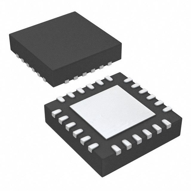
Available in Small 24-pin WQFN Package
2 Applications
•
•
•
•
High-Fidelity (HiFi) Headphone Drivers
Professional Audio Equipment
Analog and Digital Mixing Consoles
Audio Test and Measurement
The INA1620 operates over a very wide supply range
of ±2 V to ±18 V on only 2.6 mA of supply current per
channel. The INA1620 also has a shutdown mode,
allowing the amplifiers to be switched from normal
operation to a standby current that is typically less
than 5 µA. Shutdown mode is specifically designed to
eliminate click-and-pop noise when transitioning into
or out of shutdown mode.
The INA1620 has a unique internal layout for lowest
crosstalk, and freedom from interactions between
channels, even when overdriven or overloaded. This
device is specified from –40°C to +125°C.
Device Information(1)
PART NUMBER
INA1620
WQFN (24)
R2A
R2B
IN- A
IN+ A
R1B
R1A
FFT: 1 kHz, 32-Ω Load, 50 mW
±20
±40
R2C
1k
VCC
±
+
OUT A
GND
EN
4mm X 4mm QFN
Package
NC
NC
Amplitude (dBc)
R1C
EMI Filtering
4.00 mm × 4.00 mm
0
1k
1k
BODY SIZE (NOM)
(1) For all available packages, see the package option addendum
at the end of the data sheet.
INA1620 Simplified Internal Schematic
1k
PACKAGE
±60
±80
±100
-133.6 dBc (Second Harmonic)
±120
±140
±160
±
+
VEE
OUT B
±180
0
EMI Filtering
1k
1k
R4C
R3C
10k
Frequency (Hz)
15k
20k
C005
R3A
R3B
IN- B
IN+ B
1k
R4B
R4A
1k
5k
1
An IMPORTANT NOTICE at the end of this data sheet addresses availability, warranty, changes, use in safety-critical applications,
intellectual property matters and other important disclaimers. PRODUCTION DATA.
�INA1620
SBOS859B – MARCH 2018 – REVISED JULY 2018
www.ti.com
Table of Contents
1
2
3
4
5
6
7
Features ..................................................................
Applications ...........................................................
Description .............................................................
Revision History.....................................................
Pin Configuration and Functions .........................
Specifications.........................................................
1
1
1
2
3
4
6.1
6.2
6.3
6.4
6.5
6.6
4
4
4
4
5
7
Absolute Maximum Ratings ......................................
ESD Ratings..............................................................
Recommended Operating Conditions.......................
Thermal Information ..................................................
Electrical Characteristics: ........................................
Typical Characteristics ..............................................
Detailed Description ............................................ 15
7.1
7.2
7.3
7.4
Overview .................................................................
Functional Block Diagram .......................................
Feature Description.................................................
Device Functional Modes........................................
15
15
15
18
8
Application and Implementation ........................ 20
8.1 Application Information............................................ 20
8.2 Typical Application ................................................. 24
8.3 Other Application Examples.................................... 27
9 Power Supply Recommendations...................... 28
10 Layout................................................................... 28
10.1 Layout Guidelines ................................................. 28
10.2 Layout Example .................................................... 28
11 Device and Documentation Support ................. 29
11.1
11.2
11.3
11.4
11.5
11.6
11.7
Device Support......................................................
Documentation Support ........................................
Receiving Notification of Documentation Updates
Community Resources..........................................
Trademarks ...........................................................
Electrostatic Discharge Caution ............................
Glossary ................................................................
29
29
29
29
30
30
30
12 Mechanical, Packaging, and Orderable
Information ........................................................... 30
4 Revision History
NOTE: Page numbers for previous revisions may differ from page numbers in the current version.
Changes from Original (March 2018) to Revision A
•
2
Page
First release of production-data data sheet ........................................................................................................................... 1
Submit Documentation Feedback
Copyright © 2018, Texas Instruments Incorporated
Product Folder Links: INA1620
�INA1620
www.ti.com
SBOS859B – MARCH 2018 – REVISED JULY 2018
5 Pin Configuration and Functions
R1A
R1B
IN+ A
IN- A
R2B
R2A
RTW Package
24-Pin QFN
Top View
24
23
22
21
20
19
R1C
1
18
R2C
VCC
2
17
OUT A
GND
3
16
EN
Thermal
Pad
5
14
OUT B
R4C
6
13
R3C
8
9
10
11
12
R3A
7
R3B
VEE
IN- B
NC
IN+ B
15
R4B
4
R4A
NC
Pin Functions
PIN
NAME
NO.
I/O
DESCRIPTION
GND
3
—
EN
16
I
Shutdown (logic low), enable (logic high)
IN+ A
22
I
Noninverting input, channel A
IN- A
21
I
Inverting input, channel A
IN+ B
9
I
Noninverting input, channel B
IN- B
10
I
Inverting input, channel B
NC
4
—
No internal connection
NC
15
—
No internal connection
OUT A
17
O
Output, channel A
OUT B
14
O
Output, channel B
R1A
24
—
Resistor pair 1, end point A
R1B
23
—
Resistor pair 1, center point
R1C
1
—
Resistor pair 1, end point C
R2A
19
—
Resistor pair 2, end point A
R2B
20
—
Resistor pair 2, center point
R2C
18
—
Resistor pair 2, end point C
R3A
12
—
Resistor pair 3, end point A
R3B
11
—
Resistor pair 3, center point
R3C
13
—
Resistor pair 3, end point C
R4A
7
—
Resistor pair 4, end point A
R4B
8
—
Resistor pair 4, center point
R4C
6
—
Resistor pair 4, end point C
V+
2
—
Positive (highest) power supply
V–
5
—
Negative (lowest) power supply
Thermal pad
Connect to ground
Exposed thermal die pad on underside; connect thermal die pad to V–.
Submit Documentation Feedback
Copyright © 2018, Texas Instruments Incorporated
Product Folder Links: INA1620
3
�INA1620
SBOS859B – MARCH 2018 – REVISED JULY 2018
www.ti.com
6 Specifications
6.1 Absolute Maximum Ratings
over operating free-air temperature range (unless otherwise noted) (1)
MIN
MAX
Supply voltage, VS = (V+) – (V–)
Voltage
Input voltage (signal inputs, enable, ground)
Current
(V–) – 0.5
±0.5
Input current (all pins except power-supply and resistor pins)
±10
Through each resistor
30
–55
mA
125
Junction, TJ
150
Storage, Tstg
(2)
V
Continuous
Operating, TA
(1)
(V+) + 0.5
Input differential voltage
Output short-circuit (2)
Temperature
UNIT
40
–65
°C
150
Stresses beyond those listed under Absolute Maximum Ratings may cause permanent damage to the device. These are stress ratings
only, which do not imply functional operation of the device at these or any other conditions beyond those indicated under Recommended
Operating Conditions. Exposure to absolute-maximum-rated conditions for extended periods may affect device reliability.
Short-circuit to VS / 2 (ground in symmetrical dual supply setups), one amplifier per package.
6.2 ESD Ratings
VALUE
V(ESD)
(1)
(2)
Electrostatic discharge
Human-body model (HBM), per ANSI/ESDA/JEDEC JS-001 (1)
±4000
Charged-device model (CDM), per JEDEC specification JESD22-C101 (2)
±1000
UNIT
V
JEDEC document JEP155 states that 500-V HBM allows safe manufacturing with a standard ESD control process.
JEDEC document JEP157 states that 250-V CDM allows safe manufacturing with a standard ESD control process.
6.3 Recommended Operating Conditions
over operating free-air temperature range (unless otherwise noted)
MIN
Single-supply
Supply voltage, (V+) – (V–)
Dual-supply
NOM
MAX
4
36
±2
±18
Current per resistor
Specified temperature
–40
UNIT
V
15
mA
125
°C
6.4 Thermal Information
INA1620
THERMAL METRIC (1)
RTW (QFN)
UNIT
24 PINS
RθJA
Junction-to-ambient thermal resistance
33.7
°C/W
RθJC(top)
Junction-to-case (top) thermal resistance
26.5
°C/W
RθJB
Junction-to-board thermal resistance
13.1
°C/W
ψJT
Junction-to-top characterization parameter
0.3
°C/W
ψJB
Junction-to-board characterization parameter
13.1
°C/W
RθJC(bot)
Junction-to-case (bottom) thermal resistance
3.8
°C/W
(1)
4
For more information about traditional and new thermal metrics, see the Semiconductor and IC Package Thermal Metrics application
report, SPRA953.
Submit Documentation Feedback
Copyright © 2018, Texas Instruments Incorporated
Product Folder Links: INA1620
�INA1620
www.ti.com
6.5
SBOS859B – MARCH 2018 – REVISED JULY 2018
Electrical Characteristics:
at TA = 25°C, VS = ±2 V to ±18 V, VCM = VOUT = midsupply, and RL = 1 kΩ (unless otherwise noted)
PARAMETER
TEST CONDITIONS
MIN
TYP
MAX
UNIT
AUDIO PERFORMANCE
THD+N
IMD
Total harmonic distortion +
noise
Intermodulation distortion
G = 1, f = 1 kHz, VOUT = 3.5 VRMS, RL = 2 kΩ,
80-kHz measurement bandwidth
0.000025%
G = 1, f = 1 kHz, VOUT = 3.5 VRMS, RL = 600 Ω,
80-kHz measurement bandwidth
0.000025%
G = 1, f = 1 kHz, POUT = 10 mW, RL = 128 Ω,
80-kHz measurement bandwidth
0.000071%
G = 1, f = 1 kHz, POUT = 10 mW, RL = 32 Ω,
80-kHz measurement bandwidth
0.000158%
G = 1, f = 1 kHz, POUT = 10 mW, RL = 16 Ω,
80-kHz measurement bandwidth
0.000224%
SMPTE/DIN two-tone, 4:1 (60 Hz and 7 kHz),
G = 1, VO = 3 VRMS, RL = 2 kΩ, 90-kHz measurement
bandwidth
0.000018%
CCIF twin-tone (19 kHz and 20 kHz), G = 1,
VO = 3 VRMS, RL = 2 kΩ, 90-kHz measurement bandwidth
0.000032%
–132
dB
–132
dB
–123
dB
–116
dB
–113
dB
–135
dB
–130
dB
FREQUENCY RESPONSE
G = 1000
32
GBW
Gain-bandwidth product
SR
Slew rate
G = –1
10
V/μs
Full-power bandwidth (1)
VO = 1 VP
1.6
MHz
Overload recovery time
G = –10
300
ns
Channel separation (dual)
f = 1 kHz
140
dB
500
MHz
f = 20 Hz to 20 kHz
2.1
μVPP
f = 10 Hz
6.5
f = 100 Hz
3.5
f = 1 kHz
2.8
f = 10 Hz
1.6
f = 1 kHz
0.8
G=1
MHz
8
EMI filter corner frequency
NOISE
Input voltage noise
Input voltage noise density (2)
en
In
Input current noise density
nV/√Hz
pA/√Hz
OFFSET VOLTAGE
VOS
Input offset voltage
dVOS/dT
Input offset voltage drift (2)
PSRR
Power-supply rejection ratio
±0.1
TA = –40°C to 125°C
±1
±1.2
TA = –40°C to 125°C
mV
-0.5
±2.5
μV/°C
0.1
3
μV/V
INPUT BIAS CURRENT
IB
Input bias current
IOS
Input offset current
1.2
TA = –40°C to 125°C (2)
2
2.2
±10
TA = –40°C to 125°C (2)
±100
±140
μA
nA
INPUT VOLTAGE RANGE
VCM
Common-mode voltage range
CMRR
(1)
(2)
Common-mode rejection ratio
(V–) + 1.5
(V–) + 1.5 V ≤ VCM ≤ (V+) – 1 V, TA = –40°C to 125°C, VS
= ±18 V
108
(V+) – 1
127
V
dB
Full-power bandwidth = SR / (2π × VP), where SR = slew rate.
Specified by design and characterization.
Submit Documentation Feedback
Copyright © 2018, Texas Instruments Incorporated
Product Folder Links: INA1620
5
�INA1620
SBOS859B – MARCH 2018 – REVISED JULY 2018
www.ti.com
Electrical Characteristics: (continued)
at TA = 25°C, VS = ±2 V to ±18 V, VCM = VOUT = midsupply, and RL = 1 kΩ (unless otherwise noted)
PARAMETER
TEST CONDITIONS
MIN
TYP
MAX
UNIT
INPUT IMPEDANCE
Differential
Common-mode
60k || 0.8
Ω || pF
500M || 0.9
Ω || pF
OPEN-LOOP GAIN
AOL
Open-loop voltage gain
(V–) + 2 V ≤ VO ≤ (V+) – 2 V, RL = 32 Ω, VS = ± 5 V
114
120
(V–) + 1.5 V ≤ VO ≤ (V+) – 1.5 V, RL = 600 Ω, VS = ± 18 V
120
136
dB
OUTPUT
No load
Positive rail
VO
800
RL = 600 Ω
Voltage output swing from rail
1000
No load
Negative rail
mV
800
RL = 600 Ω
1000
IOUT
Output current
Figure 38
ZO
Open-loop output impedance
Figure 40
ISC
Short-circuit current
CLOAD
Capacitive load drive
VS = ±18 V
+145 / –130
mA
Ω
mA
Figure 24
pF
ENABLE PIN
VIH
Logic high threshold
VIL
Logic low threshold
IIH
Input current
0.82
TA = –40°C to 125°C (2)
0.95
0.78
TA = –40°C to 125°C (2)
V
0.65
VEN = 1.8 V
V
1.5
μA
RESISTOR PAIRS
Resistor ratio matching (3)
Resistor ratio matching
temperature coefficient
Resistors in same pair
0.004%
TA = –40°C to 125°C (2)
0.02%
0.023%
Resistors in same pair
Individual resistor value
0.84
Individual resistor temperature
coefficient
±0.07
±0.15
ppm/°C
1
1.15
kΩ
2
20
2.6
3.3
ppm/°C
POWER SUPPLY
IQ
Quiescent current
(per channel)
VEN = 2 V, IOUT = 0 A
TA = –40°C to 125°C (2)
VEN = 0 V, IOUT = 0 A
(3)
6
4.2
5
10
mA
μA
Resistor ratio matching refers to the matching between the two 1-kΩ resistors in each resistor pair. There are four pairs on each
INA1620: RXA, RXB, RXC and RXD, where X is the terminal connection number. See Resistor Tolerance for more details.
Submit Documentation Feedback
Copyright © 2018, Texas Instruments Incorporated
Product Folder Links: INA1620
�INA1620
www.ti.com
SBOS859B – MARCH 2018 – REVISED JULY 2018
6.6 Typical Characteristics
20
22
18
20
16
18
14
16
Amplifiers ( )
Amplifiers (%)
at TA = 25°C, VS = ±18 V, and RL = 2 kΩ (unless otherwise noted)
12
10
8
14
12
10
8
6
6
2
0
0
-1.5
-1.4
-1.3
-1.2
-1.1
-1
-0.9
-0.8
-0.7
-0.6
-0.5
-0.4
-0.3
-0.2
-0.1
0
0.1
0.2
0.3
0.4
0.5
0.6
0.7
0.8
0.9
1.0
4
2
-1000
-900
-800
-700
-600
-500
-400
-300
-200
-100
0
100
200
300
400
500
600
700
800
900
1000
4
D027
D030
VOS (PV)
VOS Drift (PV/qC)
9818 channels
50 channels
Figure 1. Input Offset Voltage Histogram
Figure 2. Input Offset Voltage Drift Histogram
300
±60
±62
200
±66
VOS (µV)
100
VOS ( V)
VCM = -16.5 V
±64
0
±68
VCM = 17 V
±70
±72
±100
±74
±76
±200
±78
±80
±300
±75
±50
±25
0
25
50
75
100
125
Temperature (ƒC)
±20
150
0
±10
10
20
VCM (V)
C001
C001
4 typical units
Figure 4. Input Offset Voltage vs Common-Mode Voltage
Figure 3. Input Offset Voltage vs Temperature
10
&XUUHQW 1RLVH 6SHFWUDO 'HQVLW\ S$ ¥+]
9ROWDJH 1RLVH 6SHFWUDO 'HQVLW\ Q9 ¥+]
100
10
+31
-31
1
1
10
100
1k
10k
100k
Frequency (Hz)
1M
10M
100M
1
0.1
1
Figure 5. Input Voltage Noise Spectral Density vs Frequency
10
100
1k
10k
100k
1M
10M
Frequency (Hz)
C307
100M
C306
Figure 6. Input Current Noise Spectral Density vs Frequency
Submit Documentation Feedback
Copyright © 2018, Texas Instruments Incorporated
Product Folder Links: INA1620
7
�INA1620
SBOS859B – MARCH 2018 – REVISED JULY 2018
www.ti.com
Typical Characteristics (continued)
at TA = 25°C, VS = ±18 V, and RL = 2 kΩ (unless otherwise noted)
50 nV/div
9ROWDJH 1RLVH 6SHFWUDO 'HQVLW\ Q9 ¥+]
1000
Time (2 s/div)
Source Resistor Noise Contribution
100
10
Total Noise
1
Voltage Noise Contribution
Current Noise Contribution
0.1
10
100
1k
Figure 7. 0.1-Hz to 10-Hz Noise
C302
225
120
180
100
12
10
8
6
VS = ±5V
80
40
90
20
4
VS = ±2V
2
135
60
0
0
±20
10k
Phase (º)
VS = ±15V
14
Gain (dB)
Output Amplitude (VP)
1M
140
16
100k
1M
10M
Frequency (Hz)
1
10
100
1k
10k
100k
1M
45
10M 100M
Frequency (Hz)
C303
Figure 9. Maximum Output Voltage vs Frequency
C005
Figure 10. Open-Loop Gain and Phase vs Frequency
5.0
5.0
4.0
4.0
VS = ±2 V
3.0
3.0
2.0
2.0
AOL (µV/V)
AOL (µV/V)
100k
Figure 8. Voltage Noise vs Source Resistance
18
1.0
0.0
VS = ±18 V
±1.0
VS = ±2 V
1.0
0.0
VS = ±18 V
±1.0
±2.0
±2.0
±3.0
±3.0
±4.0
±4.0
±5.0
±5.0
±75
±50
±25
0
25
50
75
100
125
Temperature (ƒC)
150
±75
±50
±25
0
25
50
75
100
125
Temperature (ƒC)
C001
600-Ω load
150
C001
2-kΩ load
Figure 11. Open-Loop Gain vs Temperature
8
10k
Source Resistance ( )
C017
Figure 12. Open-Loop Gain vs Temperature
Submit Documentation Feedback
Copyright © 2018, Texas Instruments Incorporated
Product Folder Links: INA1620
�INA1620
www.ti.com
SBOS859B – MARCH 2018 – REVISED JULY 2018
Typical Characteristics (continued)
at TA = 25°C, VS = ±18 V, and RL = 2 kΩ (unless otherwise noted)
40
Total Harmonic Distortion + Noise (%)
Gain (dB)
20
0
-20
0.01
-80
G = -1, 600- Load
G = -1, 2k- Load
G = -1, 10k- Load
G = +1, 600- Load
G = +1, 2k- Load
G = +1, 10k- Load
0.001
-100
-120
0.0001
-140
20k
0.00001
100
1k
10k
100k
1M
10M
Frequency (Hz)
20
200
2k
Frequency (Hz)
C004
Total Harmonic Distortion + Noise (dB)
G = +10
G = -1
G = +1
C004
3.5 VRMS, 80-kHz measurement bandwidth
0.01
-80
0.001
-100
0.0001
-120
-140
20k
0.00001
20
200
2k
Frequency (Hz)
Total Harmonic Distortion + Noise (%)
-60
G = -1, 128- Load
G = -1, 32- Load
G = -1, 16- Load
G = +1, 128- Load
G = +1, 32- Load
G = +1, 16- Load
0.01
0.0001
-140
1
10
Output Amplitude (VRMS)
10
Output Amplitude (VRMS)
0.1
Intermodulation Distortion (%)
Total Harmonic Distortion + Noise (%)
-120
128- Load
32- Load
16- Load
1
C004
-80
0.01
SMPTE
-100
0.001
-120
0.0001
CCIF
0.00001
0.001
-140
0.01
0.1
1
10
Output Amplitude (VRMS)
C004
1 kHz, 80-kHz measurement bandwidth
Figure 17. THD+N Ratio vs Output Amplitude
-60
2k- Load
32- Load
Intermodulation Distortion (dB)
Noninverting
Total Harmonic Distortion + Noise (dB)
-100
0.0001
-140
0.1
Figure 16. THD+N Ratio vs Output Amplitude
-80
0.001
0.1
2k- Load
600- Load
1 kHz, 80-kHz measurement bandwidth
-60
Inverting
-120
Noninverting
0.00001
0.01
Figure 15. THD+N Ratio vs Frequency
0.00001
0.01
-100
C004
0.1
-80
Inverting
0.001
10 mW, 80-kHz measurement bandwidth
0.01
-60
0.1
Total Harmonic Distortion + Noise (dB)
0.1
Figure 14. THD+N Ratio vs Frequency
Total Harmonic Distortion + Noise (dB)
Total Harmonic Distortion + Noise (%)
Figure 13. Closed-Loop Gain vs Frequency
C004
90-kHz measurement bandwidth
Figure 18. Intermodulation Distortion vs Output Amplitude
Submit Documentation Feedback
Copyright © 2018, Texas Instruments Incorporated
Product Folder Links: INA1620
9
�INA1620
SBOS859B – MARCH 2018 – REVISED JULY 2018
www.ti.com
Typical Characteristics (continued)
at TA = 25°C, VS = ±18 V, and RL = 2 kΩ (unless otherwise noted)
160
-80
Crosstalk (dB)
-100
Power Supply Rejection Ratio (dB)
No Load
32- Load
600- Load
-120
-140
120
80
60
40
20
0
100
1k
10k
100k
1M
10M
Frequency (Hz)
1
100
1k
10k
100k
1M
Frequency (Hz)
Figure 19. Channel Separation vs Frequency
10M
C115
Figure 20. PSRR vs Frequency (Referred to Input)
140
Common-mode Rejection Ratio (dB)
Power-Supply Rejection Ratio (µV/V)
10
C004
5
4
3
2
1
0
-1
-2
-3
-4
120
100
-5
80
60
40
20
0
±75
±50
0
±25
25
50
75
100
125
Temperature (ƒC)
150
1
10
100
1k
10k
100k
1M
Frequency (Hz)
C001
Figure 21. PSRR vs Temperature
10M
C004
Figure 22. CMRR vs Frequency (Referred to Input)
90
1
0.8
” 9CM ” 9
VS = ±2 V, (V±)
±1V
80
0.6
G = +1
70
0.4
Phase Margin (º)
Common-Mode Rejection Ratio (µV/V)
PSRR-
100
-160
0.2
0
” 9CM ” 9
VS = ±18 V, (V±)
-0.2
± 1V
-0.4
60
G = -1
50
40
30
20
-0.6
10
-0.8
0
-1
±75
±50
±25
0
25
50
75
100
Temperature (ƒC)
125
150
0
200
400
600
800
Capacitive Load (pF)
C001
Figure 23. CMRR vs Temperature
10
PSRR+
140
1000
C308
Figure 24. Phase Margin vs Capacitive Load
Submit Documentation Feedback
Copyright © 2018, Texas Instruments Incorporated
Product Folder Links: INA1620
�INA1620
www.ti.com
SBOS859B – MARCH 2018 – REVISED JULY 2018
Typical Characteristics (continued)
2 V/div
2 mV/div
at TA = 25°C, VS = ±18 V, and RL = 2 kΩ (unless otherwise noted)
Time (2.5 s/div)
Time (2.5 s/div)
C017
C017
G = 1, 10 mV
G = 1, 10 V
Figure 25. Small-Signal Step Response
Figure 26. Large-Signal Step Response
VOUT
5 V/div
5 V/div
VIN
VIN
VOUT
Time (200 ns/div)
Time (200 ns/div)
C017
C017
G = –10
G = –10
Figure 27. Negative Overload Recovery
Figure 28. Positive Overload Recovery
1.5
5 V/div
Input Bias Current ( A)
1.4
VOUT
VIN
1.3
1.2
1.1
1
IBIB+
0.9
Time (500 ms/div)
±50
C017
Figure 29. No Phase Reversal
±25
0
25
50
75
100
Temperature (ºC)
125
C304
Figure 30. IB vs Temperature
Submit Documentation Feedback
Copyright © 2018, Texas Instruments Incorporated
Product Folder Links: INA1620
11
�INA1620
SBOS859B – MARCH 2018 – REVISED JULY 2018
www.ti.com
Typical Characteristics (continued)
at TA = 25°C, VS = ±18 V, and RL = 2 kΩ (unless otherwise noted)
1.5
Input Bias Current ( A)
Input Offset Current (nA)
5
4
3
2
1.4
1.3
1.2
1.1
1
1
±50
0
±25
25
50
75
100
125
Temperature (ºC)
-20
-10
0
10
20
Common-Mode Voltage (V)
C305
C001
VS = ±18 V
Figure 31. IOS vs Temperature
Figure 32. IB vs Common-Mode Voltage
5
1.3
4
1.25
3.5
IQ (mA)
Input Bias Current ( A)
4.5
1.2
VS = ±18 V
3
VS = ±2 V
2.5
2
1.5
1.15
1
0.5
0
1.1
-1.5
-1
-0.5
0
0.5
1
±75
1.5
Common-Mode Voltage (V)
±50
±25
0
25
50
75
100
125
150
Temperature (ƒC)
C002
C001
VS = ±2 V
Figure 34. Quiescent Current vs Temperature
Figure 33. IB vs Common-Mode Voltage
3
5
2.5
4
125ºC
85ºC
IQ (mA)
IQ (mA)
2
1.5
3
2
-40ºC
1
1
0.5
0
0
0
2
4
6
8
10
12
14
16
18
Supply Voltage (V)
20
0.5
1
1.5
Enable Voltage (V)
C001
Figure 35. Quiescent Current vs Supply Voltage
12
25ºC
2
C002
Figure 36. Quiescent Current vs Enable Voltage
Submit Documentation Feedback
Copyright © 2018, Texas Instruments Incorporated
Product Folder Links: INA1620
�INA1620
www.ti.com
SBOS859B – MARCH 2018 – REVISED JULY 2018
Typical Characteristics (continued)
at TA = 25°C, VS = ±18 V, and RL = 2 kΩ (unless otherwise noted)
18
200
16
180
14
ISC, Source
160
12
VO (V)
ISC (mA)
140
120
10
8
6
ISC, Sink
100
125°C
25°C
4
80
±40°C
0
60
±75
±50
0
±25
25
50
75
100
125
0
150
Temperature (ƒC)
20
40
60
80
100 120 140 160 180 200
IO (mA)
C001
C001
Figure 38. Positive Output Voltage vs Output Current
Figure 37. Short-Circuit Current vs Temperature
0
100
-2
125°C
25°C
-4
85°C
-6
±40°C
-8
ZO ( )
VO (V)
85°C
2
-10
10
-12
-14
-16
-18
1
0
20
40
60
80
100 120 140 160 180 200
IO (mA)
1
100
18
22.5
16
20
14
17.5
Resistors (%)
25
10
8
10k
100k
1M
10M
100M
C001
Figure 40. Open-Loop Output Impedance vs Frequency
20
12
1k
Frequency (Hz)
Figure 39. Negative Output Voltage vs Output Current
15
12.5
10
0.02
0.016
0.012
0.008
0.004
D026
0
0
-0.004
0
-0.008
2
-0.016
5
2.5
925
930
935
940
945
950
955
960
965
970
975
980
985
990
995
1000
1005
1010
1015
1020
1025
4
-0.012
7.5
6
-0.02
Resistors (%)
10
C001
D028
Resistance (:)
Resistor Ratio Matching Error (%)
19635 resistors
19639 resistor pairs
Figure 41. Resistor Absolute Value Histogram
Figure 42. Resistor Pair Matching Histogram
Submit Documentation Feedback
Copyright © 2018, Texas Instruments Incorporated
Product Folder Links: INA1620
13
�INA1620
SBOS859B – MARCH 2018 – REVISED JULY 2018
www.ti.com
Typical Characteristics (continued)
at TA = 25°C, VS = ±18 V, and RL = 2 kΩ (unless otherwise noted)
27.5
25
Resistor Pairs ( )
22.5
20
17.5
15
12.5
10
7.5
5
2.5
-0.15
-0.14
-0.13
-0.12
-0.11
-0.1
-0.09
-0.08
-0.07
-0.06
-0.05
-0.04
-0.03
-0.02
-0.01
0
0.01
0.02
0.03
0.04
0.05
0
D029
Resistor Ratio Matching Drift (ppm/qC)
64 resistor pairs
Figure 43. Resistor Pair Matching Drift Histogram
14
Submit Documentation Feedback
Copyright © 2018, Texas Instruments Incorporated
Product Folder Links: INA1620
�INA1620
www.ti.com
SBOS859B – MARCH 2018 – REVISED JULY 2018
7 Detailed Description
7.1 Overview
The INA1620 integrates a dual, bipolar-input, audio operational amplifier with four high-precision thin-film resistor
pairs on the same die. The internal amplifiers and resistor pairs are pinned out to allow for many circuit
configurations.
The internal amplifiers of the INA1620 use a unique topology to deliver high output current with extremely low
distortion while consuming minimal supply current. A single gain-stage architecture, combining a high-gain
transconductance input stage and a unity-gain output stage, allows the INA1620 to achieve an open-loop gain of
136 dB, even with 600-Ω loads.
A separate enable circuit maintains control of the input and output stage when the amplifier is placed into its
shutdown mode and limits transients at the amplifier output when transitioning to and from this state. The enable
circuit features logic levels referenced to the amplifier ground pin. This configuration simplifies the interface
between the amplifier and the ground-referenced GPIO pins of microcontrollers. The addition of a ground pin to
the amplifier provides several additional benefits. For example, the compensation capacitor between the input
and output stages of the INA1620 is referenced to the ground pin, greatly improving PSRR.
1k
R2A
R2B
IN- A
IN+ A
R1B
R1A
7.2 Functional Block Diagram
1k
R1C
R2C
1k
1k
EMI Filtering
VCC
±
+
OUT A
GND
EN
4mm X 4mm QFN
Package
NC
NC
±
+
VEE
OUT B
EMI Filtering
1k
1k
R4C
R3C
R3A
R3B
IN- B
IN+ B
1k
R4B
R4A
1k
7.3 Feature Description
7.3.1 Matched Thin-Film Resistor Pairs
The INA1620 integrates four thin-film resistor pairs. Each pair is made up of two thin-film resistors with a nominal
resistance of 1 kΩ. While the absolute value of the resistor is not trimmed and can vary significantly, the two
resistors in an pair are designed to match each other extremely well. The resistors in an pair typically match to
within 0.004% of each other's value. This matching is also preserved well over temperature, with the matching
drift having a 0.2 ppm/°C maximum specification. Each node in the resistor pair is bonded out to a pad on the
Submit Documentation Feedback
Copyright © 2018, Texas Instruments Incorporated
Product Folder Links: INA1620
15
�INA1620
SBOS859B – MARCH 2018 – REVISED JULY 2018
www.ti.com
Feature Description (continued)
INA1620 package allowing the resistor pairs to be used in multiple configurations. The nodes in the pair are
protected from damage due to electrostatic discharge (ESD) events by diodes tied to the power supplies of the
IC. For this reason, voltages beyond the power supplies cannot be applied to the resistors without forwardbiasing the ESD protection diodes. The resistor pairs should not be used if there is no power applied to the
INA1620. The configuration of the ESD protection diodes is shown in Figure 44.
V+
V+
V+
1k
1k
RxC
RxA
V-
V-
V-
RxB
Figure 44. ESD Protection Diodes on Each Resistor Pair
Although the resistor pairs and amplifier core are fabricated on the same silicon substrate, they can be used in
separate circuits as long as the previously-mentioned voltage limits are observed. The functional state of the
amplifier (enabled or shutdown) does not affect the resistor pair's performance.
7.3.2 Power Dissipation
The INA1620 is capable of high output current with power-supply voltages up to ±18 V. Internal power dissipation
increases when operating at high supply voltages. The power dissipated in the op amp (POPA) is calculated using
Equation 1:
V
POPA
V VOUT u IOUT
V VOUT u OUT
RL
(1)
In order to calculate the worst-case power dissipation in the op amp, the ac and dc cases must be considered
separately.
In the case of constant output current (dc) to a resistive load, the maximum power dissipation in the op amp
occurs when the output voltage is half the positive supply voltage. This calculation assumes that the op amp is
sourcing current from the positive supply to a grounded load. If the op amp sinks current from a grounded load,
modify Equation 2 to include the negative supply voltage instead of the positive.
POPA(MAX _ DC)
§V ·
POPA ¨
¸
© 2 ¹
V2
4RL
(2)
The maximum power dissipation in the op amp for a sinusoidal output current (ac) to a resistive load occurs
when the peak output voltage is 2/π times the supply voltage, given symmetrical supply voltages:
POPA(MAX _ AC)
§ 2V ·
POPA ¨
¸
© S ¹
2˜V
2
S2 ˜ RL
(3)
The dominant pathway for the INA1620 to dissipate heat is through the package thermal pad and pins to the
PCB. Copper leadframe construction used in the INA1620 improves heat dissipation compared to conventional
materials. PCB layout greatly affects thermal performance. Connect the INA1620 package thermal pad to a
copper pour at the most negative supply potential. This copper pour can be connected to a larger copper plane
within the PCB using vias to improve power dissipation. Figure 45 shows an analogous thermal circuit that can
be used for approximating the junction temperature of the INA1620. The power dissipated in the INA1620 is
represented by current source PD; the ambient temperature is represented by voltage source 25ºC; and the
junction-to-board and board-to-ambient thermal resistances are represented by resistors RθJB and RθBA,
respectively. The board-to-ambient thermal resistance is unique to every application. The sum of RθJB and RθBA is
the junction-to-ambient thermal resistance of the system. The value for junction-to-ambient thermal resistance
reported in the Thermal Information table is determined using the JEDEC standard test PCB. The voltages in the
analogous thermal circuit at the points TJ and TPCB represent the INA1620 junction and PCB temperatures,
respectively.
16
Submit Documentation Feedback
Copyright © 2018, Texas Instruments Incorporated
Product Folder Links: INA1620
�INA1620
www.ti.com
SBOS859B – MARCH 2018 – REVISED JULY 2018
Feature Description (continued)
TJ
,JB
TPCB
PD
,BA
25ºC
Figure 45. Approximate Thermal System Model of the INA1620 Soldered to a PCB
7.3.3 Thermal Shutdown
If the junction temperature of the INA1620 exceeds 175°C, a thermal shutdown circuit disables the amplifier in
order to protect the device from damage. The amplifier is automatically re-enabled after the junction temperature
falls below approximately 160°C. If the condition that caused excessive power dissipation has not been removed,
the amplifier oscillates between a shutdown and enabled state until the output fault is corrected.
7.3.4 EN Pin
The enable pin (EN) of the INA1620 is used to toggle the amplifier enabled and disabled states. The logic levels
defining these two states are: VEN ≤ 0.78 V (shutdown mode), and VEN ≥ 0.82 V (enabled). These threshold
levels are referenced to the device ground (GND) pin. The EN pin can be driven by a GPIO pin from the system
controller, discrete logic gates, or can be connected directly to the V+ supply. Do not leave the EN pin floating
because the amplifier is prevented from being enabled. Likewise, do not place GPIO pins used to control the EN
pin in a high-impedance state because this placement also prevents the amplifier from being enabled. A small
current flows into the enable pin when a voltage is applied. Using the simplified internal schematic shown in
Figure 46, use Equation 4 to estimate the enable pin current:
VEN 0.7 V
IEN
700 k
(4)
As illustrated in Figure 46, the EN pin is protected by diodes to the amplifier power supplies. Do not connect the
EN pin to voltages outside the limits defined in the Specifications section.
To
Amplifier
VCC
500 k
EN
VEE
VCC
200 k
GND
VEE
Figure 46. EN Pin Simplified Internal Schematic
Submit Documentation Feedback
Copyright © 2018, Texas Instruments Incorporated
Product Folder Links: INA1620
17
�INA1620
SBOS859B – MARCH 2018 – REVISED JULY 2018
www.ti.com
Feature Description (continued)
7.3.5 GND Pin
The inclusion of a ground (GND) pin in the INA1620 architecture allows the internal enable circuitry to be
referenced to the system ground, eliminating the need for level shifting circuitry in many applications. The internal
amplifier compensation capacitors are also referenced to this pin, greatly increasing the ac PSRR. For highest
performance, connect the GND pin to a low-impedance reference point with minimal noise present. As shown in
Figure 46, the GND pin is protected by ESD diodes to the amplifier power supplies. Do not connect the GND pin
to voltages outside the limits defined in the Specifications section.
7.3.6 Input Protection
The amplifier input pins of the INA1620 are protected from excessive differential voltage with back-to-back
diodes, as Figure 47 shows. In most circuit applications, the input protection circuitry has no consequence.
However, in low-gain or G = +1 circuits, fast-ramping input signals can forward bias these diodes because the
output of the amplifier cannot respond quickly enough to the input ramp. If the input signal is fast enough to
create this forward-bias condition, the input signal current must be limited to 10 mA or less. If the input signal
current is not inherently limited, use an input series resistor (RI) or a feedback resistor (RF) to limit the signal
input current. This input series resistor degrades the low-noise performance of the INA1620 and is examined in
the Noise Performance section. Figure 47 shows an example configuration when both current-limiting input and
feedback resistors are used.
RF
–
Device
RI
Input
Output
+
Figure 47. Pulsed Operation
7.4 Device Functional Modes
The INA1620 has two operating modes determined by the voltage between the EN and GND pins: a shutdown
mode (VEN ≤ 0.78 V) and an enabled mode (VEN ≥ 0.82 V). The measured datasheet performance parameters
specified in the Typical Characteristics and Specifications sections are given with the amplifier in the enabled
mode, unless otherwise noted.
7.4.1 Shutdown Mode
When the EN pin voltage is below the logic low threshold, the INA1620 enters a shutdown mode with minimal
power consumption. In this state the output transistors of the amplifier are not powered on. However, do not
consider the amplifier output to be high-impedance. Applying signals to the output of the INA1620 while the
device is in the shutdown mode can parasitically power the output stage, causing the INA1620 output to draw
current.
The INA1620 enable circuitry limits transients at the output when transitioning into or out of shutdown mode.
However, small output transients do still accompany this transition, as illustrated in Figure 48 and Figure 49. Note
that in both figures the time scale is 1 µs per division, indicating that the output transients are extremely brief in
nature, and therefore not likely to be audible in headphone applications.
18
Submit Documentation Feedback
Copyright © 2018, Texas Instruments Incorporated
Product Folder Links: INA1620
�INA1620
www.ti.com
SBOS859B – MARCH 2018 – REVISED JULY 2018
Device Functional Modes (continued)
Enable (2 V/div)
Voltage
Voltage
Enable (2 V/div)
Output (20 mV/div)
Output (20 mV/div)
Time (1 s/div)
Time (1 s/div)
C001
C002
Figure 48. INA1620 Output Voltage When EN Pin
Transitions High (32-Ω Load Connected)
Figure 49. INA1620 Output Voltage When EN Pin
Transitions Low (32-Ω Load Connected)
7.4.2 Output Transients During Power Up and Power Down
To minimize the possibility of output transients that might produce an audible click or pop, ramp the supply
voltages for the INA1620 symmetrically to their nominal values. Asymmetrical supply ramping can cause output
transients during power up that can be audible in headphone applications. If possible, hold the EN pin low while
the power supplies are ramping up or down. If the EN pin is not being independently controlled (for example, by
a GPIO pin), use a voltage divider to hold the enable pin voltage below the logic-high threshold until the power
supplies reach the specified minimum voltage, as shown in Figure 50.
VCC
22.1 k
To enable
pin on IC
10.7 k
Figure 50. Voltage Divider Used to Hold Enable Low at Power-Up or Power-Down
Submit Documentation Feedback
Copyright © 2018, Texas Instruments Incorporated
Product Folder Links: INA1620
19
�INA1620
SBOS859B – MARCH 2018 – REVISED JULY 2018
www.ti.com
8 Application and Implementation
NOTE
Information in the following applications sections is not part of the TI component
specification, and TI does not warrant its accuracy or completeness. TI’s customers are
responsible for determining suitability of components for their purposes. Customers should
validate and test their design implementation to confirm system functionality.
8.1 Application Information
The low noise and distortion of the INA1620 make the device useful for a variety of applications in professional
and consumer audio products. However, these same performance metrics also make the INA1620 useful for
industrial, test-and-measurement, and data-acquisition applications. The example shown here is only one
possible application where the INA1620 provides exceptional performance.
8.1.1 Noise Performance
Figure 51 shows the total circuit noise for varying source impedances with the op amp in a unity-gain
configuration (no feedback resistor network, and therefore no additional noise contributions).
The INA1620 is shown with total circuit noise calculated. The op amp contributes both a voltage noise
component and a current noise component. The voltage noise is commonly modeled as a time-varying
component of the offset voltage. The current noise is modeled as the time-varying component of the input bias
current, and reacts with the source resistance to create a voltage component of noise. Therefore, the lowest
noise op amp for a given application depends on the source impedance. For low source impedance, current
noise is negligible, and voltage noise generally dominates. The low voltage and current noise of the INA1620
internal op amps make the device an excellent choice for use in applications where the source impedance is less
than 10 kΩ as shown in Figure 51.
9ROWDJH 1RLVH 6SHFWUDO 'HQVLW\ Q9 ¥+]
1000
Source Resistor Noise Contribution
100
10
Total Noise
1
Voltage Noise Contribution
Current Noise Contribution
0.1
10
100
1k
10k
Source Resistance ( )
100k
1M
C302
Figure 51. Noise Performance of the INA1620 Internal Amplifiers
20
Submit Documentation Feedback
Copyright © 2018, Texas Instruments Incorporated
Product Folder Links: INA1620
�INA1620
www.ti.com
SBOS859B – MARCH 2018 – REVISED JULY 2018
Application Information (continued)
8.1.2 Resistor Tolerance
The INA1620 integrated resistor pairs use an advanced thin film process to create resistor pairs that have
excellent matching. Each specific resistor pair is specifically designed for accurate matching between the two
resistors. Figure 42 shows the distribution of resistor matching for a typical device population. The equation used
to calculate matching between resistors in a pair is shown in Equation 5.
RXA RXB
Resistor Ratio Matching %
u 100
Average RXA ,RXB
(5)
In addition to excellent matching between resistors in each resistor pair, all resistors on a single INA1620 achieve
good matching due to inherent process matching across each device. Figure 52 shows a typical distribution of
the worst-case matching across all resistors on a single INA1620. The matching was calculated using the highest
value resistance on a device matched with the lowest resistance value on the same device.
22
20
18
Devices ( )
16
14
12
10
8
6
4
2
1.5
1.4
1.3
1.2
1
1.1
0.9
0.8
0.7
0.6
0.5
0.4
0.3
0.2
0.1
0
D032
Resistor Matching, Maximum to Minimum (%)
Figure 52. Matching Histogram, Maximum to Minimum
8.1.3 EMI Rejection
The electromagnetic interference (EMI) rejection ratio, or EMIRR, describes the EMI immunity of operational
amplifiers. An adverse effect that is common to many op amps is a change in the offset voltage as a result of RF
signal rectification. An op amp that is more efficient at rejecting this change in offset as a result of EMI has a
higher EMIRR and is quantified by a decibel value. Measuring EMIRR can be performed in many ways, but this
section provides the EMIRR IN+, which specifically describes the EMIRR performance when the RF signal is
applied to the noninverting input pin of the op amp. In general, only the noninverting input is tested for EMIRR for
the following three reasons:
• Op amp input pins are known to be the most sensitive to EMI, and typically rectify RF signals better than the
supply or output pins.
• The noninverting and inverting op amp inputs have symmetrical physical layouts and exhibit approximately
matching EMIRR performance.
• EMIRR is easier to measure on noninverting pins than on other pins because the noninverting input pin can
be isolated on a PCB. This isolation allows the RF signal to be applied directly to the noninverting input
terminal with no complex interactions from other components or connecting PCB traces.
High-frequency signals conducted or radiated to any pin of the operational amplifier result in adverse effects, as
the amplifier does not have sufficient loop gain to correct for signals with spectral content outside its bandwidth.
Conducted or radiated EMI on inputs, power supply, or output may result in unexpected DC offsets, transient
voltages, or other unknown behavior. Take care to properly shield and isolate sensitive analog nodes from noisy
radio signals and digital clocks and interfaces.
The EMIRR IN+ of the INA1620 amplifiers is plotted versus frequency as shown in Figure 53. See also EMI
Rejection Ratio of Operational Amplifiers, available for download from www.ti.com.
Submit Documentation Feedback
Copyright © 2018, Texas Instruments Incorporated
Product Folder Links: INA1620
21
�INA1620
SBOS859B – MARCH 2018 – REVISED JULY 2018
www.ti.com
EMIRR IN+ (dB)
Application Information (continued)
70
65
60
55
50
45
40
35
30
25
20
15
10
5
0
100M
1G
Frequency (Hz)
10G
D033
Figure 53. INA1620 EMIRR IN+
Table 1 lists the EMIRR IN+ values for the INA1620 at particular frequencies commonly encountered in realworld applications. Applications listed in Table 1 may be centered on or operated near the particular frequency
shown. This information may be of special interest to designers working with these types of applications, or
working in other fields likely to encounter RF interference from broad sources, such as the industrial, scientific,
and medical (ISM) radio band.
Table 1. INA1620 EMIRR IN+ for Frequencies of Interest
FREQUENCY
EMIRR IN+
900 MHz
18 dB
1.8 GHz
GSM applications, mobile personal communications, broadband, satellite, L-band (1 GHz to 2 GHz)
33 dB
2.4 GHz
802.11b, 802.11g, 802.11n, Bluetooth®, mobile personal communications, industrial, scientific and
medical (ISM) radio band, amateur radio and satellite, S-band (2 GHz to 4 GHz)
26 dB
3.6 GHz
Radiolocation, aero communication and navigation, satellite, mobile, S-band
40 dB
802.11a, 802.11n, aero communication and navigation, mobile communication, space and satellite
operation, C-band (4 GHz to 8 GHz)
55 dB
5 GHz
22
APPLICATION OR ALLOCATION
Global system for mobile communications (GSM) applications, radio communication, navigation,
GPS (to 1.6 GHz), GSM, aeronautical mobile, UHF applications
Submit Documentation Feedback
Copyright © 2018, Texas Instruments Incorporated
Product Folder Links: INA1620
�INA1620
www.ti.com
SBOS859B – MARCH 2018 – REVISED JULY 2018
8.1.4 EMIRR +IN Test Configuration
Figure 54 shows the circuit configuration for testing the EMIRR IN+. An RF source connects to the op amp
noninverting input pin using a transmission line. The op amp is configured in a unity-gain buffer topology with the
output connected to a low-pass filter (LPF) and a digital multimeter (DMM). A large impedance mismatch at the
op amp input causes a voltage reflection; however, this effect is characterized and accounted for when
determining the EMIRR IN+. A multimeter samples and measures the resulting DC offset voltage. The LPF
isolates the multimeter from residual RF signals that may interfere with multimeter accuracy.
Ambient temperature: 25Û&
+VS
±
50
Low-Pass Filter
+
RF source
DC Bias: 0 V
Modulation: None (CW)
Frequency Sweep: 201 pt. Log
-VS
Not shown: 0.1 µF and 10 µF
supply decoupling
Sample /
Averaging
Digital Multimeter
Figure 54. EMIRR +IN Test Configuration
Submit Documentation Feedback
Copyright © 2018, Texas Instruments Incorporated
Product Folder Links: INA1620
23
�INA1620
SBOS859B – MARCH 2018 – REVISED JULY 2018
www.ti.com
8.2 Typical Application
The low distortion and high output-current capabilities of the INA1620 make this device an excellent choice for
headphone-amplifier applications in portable or studio applications. These applications typically employ an audio
digital-to-analog converter (DAC) and a separate headphone amplifier circuit connected to the DAC output. Highperformance audio DACs can have an output signal that is either a varying current or voltage. Voltage output
configurations require less external circuitry, and therefore have advantages in cost, power consumption, and
solution size. However, these configurations can offer slightly lower performance than current output
configurations. Differential outputs are standard on both types of DACs. Differential outputs double the output
signal levels that can be delivered on a single, low-voltage supply, and also allow for even-harmonics common to
both outputs to be cancelled by external circuitry. A simplified representation of a voltage-output audio DAC is
shown in Figure 55. Two ac voltage sources (VAC) deliver the output signal to the complementary outputs
through their associated output impedances (ROUT). Both output signals have a dc component as well,
represented by dc voltage source VDC. The headphone amplifier circuit connected to the output of an audio DAC
must convert the differential output into a single-ended signal and be capable of producing signals of sufficient
amplitude at the headphones to achieve reasonable listening levels.
100 pF
ROUT
1k
1k
5V
VAC
±
+
Headphone Output
+
VDC
VAC
-5V
ROUT
1k
Audio DAC
1k
INA1620
100 pF
Figure 55. INA1620 Used as a Headphone Amplifier for a Voltage-Output Audio DAC
8.2.1 Design Requirements
•
•
•
•
±5-V power supplies
150-mW output power (32-Ω load)
< –110-dB THD+N at maximum output (32-Ω load)
< 0.01-dB magnitude deviation (20 Hz to 20 kHz)
8.2.2 Detailed Design Procedure
Figure 55 shows a schematic of a headphone amplifier circuit for voltage output DACs. An op amp is configured
as a difference amplifier that converts the differential output voltage to single-ended.
The gain of the difference amplifier in Figure 55 is determined by the resistor values, and includes the output
impedance of the DAC. For R2 = R4 and R1 = R3, the output voltage of the headphone amplifier circuit is shown
in Equation 6:
R2
VOUT VDAC
R1 ROUT
(6)
The output voltage required for headphones depends on the headphone impedance, as well as the headphone
efficiency (η), a measure of the sound pressure level (SPL, measured in dB) for a certain input power level
(typically given at 1 mW). The headphone SPL at other power levels is calculated using Equation 7:
24
Submit Documentation Feedback
Copyright © 2018, Texas Instruments Incorporated
Product Folder Links: INA1620
�INA1620
www.ti.com
SBOS859B – MARCH 2018 – REVISED JULY 2018
Typical Application (continued)
SPL(dB)
§ P
·
K 10log ¨ IN ¸
© 1 mW ¹
where
•
•
η = efficiency
PIN = input power to the headphones
(7)
Figure 56 shows the input power required to produce certain SPLs for different headphone efficiencies. Typically,
over-the-ear style headphones have lower efficiencies than in-ear types with 95 dB/mW being a common value.
150
Sound Pressure Level (SPL, dB)
140
130
120
110
100
90-dB/mW
90
95-dB/mW
100-dB/mW
80
105-dB/mW
70
110-dB/mW
115-dB/mW
60
0.01
0.1
1
10
100
1000
Input Power (mW)
C001
Figure 56. Sound Pressure Level vs Input Power for Headphones of Various Efficiencies
In-ear headphones can have efficiencies of 115 dB/mW or greater, and therefore have much lower power
requirements. The output power goal for this design is 150 mW — sufficient power to produce extremely loud
sound pressure levels in a wide range of headphones. A 32-Ω headphone impedance is used for this
requirement because 32 Ω is a very common value in headphones for portable applications. Equation 8 shows
the voltage required for 32-Ω headphones:
VO
PuR
150 mW u 32
9RMS
(8)
Capacitors C1 and C2 limit the bandwidth of the circuit to prevent the unnecessary amplification of interfering
signals. The maximum value of these capacitors is determined by the limitations on frequency response
magnitude deviation detailed in the Design Requirements section. C1 and C2 combine with resistors R2 and R4 to
form a pole, as shown in Equation 9:
1
fP
2S(R2 ,R 4 )(C1,C2 )
(9)
Calculate the minimum pole frequency allowable to meet the magnitude deviation requirements using
Equation 10:
f
20 kHz
t
t 416.6 kHz
fP t
2
2
§1·
§ 1 ·
¨G¸ 1
¨ 0.999 ¸ 1
© ¹
©
¹
where
•
G represents the gain in decimal for a –0.01-dB deviation at 20 kHz.
(10)
Submit Documentation Feedback
Copyright © 2018, Texas Instruments Incorporated
Product Folder Links: INA1620
25
�INA1620
SBOS859B – MARCH 2018 – REVISED JULY 2018
www.ti.com
Typical Application (continued)
Use Equation 11 to calculate the upper limit for the value of C1 and C2 in order to meet the goal for minimal
magnitude deviation at 20 kHz.
1
1
C1,C2 d
d
d 382 pF
2S(R2 ,R 4 )FP 2S(1 k
N+]
(11)
For this design, 100-pF capacitors were used because they meet the design requirements for amplitude
deviation in the audio bandwidth.
8.2.3 Application Curves
Figure 57 shows the maximum output voltage achievable for a 32-Ω load before the onset of clipping (±5-V
supplies), indicated by a sharp increase in distortion. As more current is delivered by the output transistors of an
amplifier, additional distortion is produced. At low frequencies, this distortion is corrected by the feedback loop of
the amplifier. However, as the loop gain of the amplifier begins to decline at high frequencies, the overall
distortion begins to climb. The unique output stage design of the INA1620 greatly reduces the additional
distortion at high frequency when delivering large currents, as shown in Figure 58. High-ordered harmonics
(above the 2nd and 3rd) are also kept to a minimal level at high output powers, as shown in Figure 59.
Left Channel
Right Channel
-70
Total Harmonic Distortion + Noise (dB)
Total Harmonic Distortion + Noise (dB)
-60
-80
-90
-100
-110
-120
0.01
0.1
Output Level (Vrms)
1
5
-80
-82
-84
-86
-88
-90
-92
-94
-96
-98
-100
-102
-104
-106
-108
-110
10
22.4-kHz measurement bandwidth
100
1k
Frequency (Hz)
10k
90-kHz measurement bandwidth, 1-VRMS output
Figure 57. THD+N vs Output Voltage for a 32-Ω Load
Amplitude (dBV)
Left Channel
Right Channel
Figure 58. THD+N vs Frequency for a 32-Ω Load
0
-10
-20
-30
-40
-50
-60
-70
-80
-90
-100
-110
-120
-130
-140
-150
0
5000
10000
Frequency (Hz)
15000
20000
1 kHz, 32-Ω load, 1 VRMS
Figure 59. Output Spectrum
26
Submit Documentation Feedback
Copyright © 2018, Texas Instruments Incorporated
Product Folder Links: INA1620
�INA1620
www.ti.com
SBOS859B – MARCH 2018 – REVISED JULY 2018
8.3 Other Application Examples
8.3.1 Preamplifier for Professional Microphones
Figure 60 shows a preamplifier designed for high performance applications that require low-noise and high
common-mode rejection. Both channels of the INA1620 are configured as a two-op amp instrumentation amplifier
with a variable gain from 6 to 40 dB. The excellent matching of the integrated 1kΩ resistors allows for high
common-mode rejection in the circuit. An OPA197 is configured as a buffered power supply divider to provide a
biasing voltage to the circuit, allowing the system to operate properly on a single 9-V battery. The additional
components at the INA1620 inputs are for phantom power, EMI, and ESD protection.
9V
9V
0.1 F
100 k
OPA197
+
VBIAS
±
1 F
100 k
10-k Potentiometer
(Logarithmic)
20
VBIAS
R3B
R2B
48 V Phantom Power
R2A
1k
R2C R3A
1k
1k
1k
R3C
9V
9V
0.1 F
47 k
6.8 k
3
D2
±
68
100
pF
30
VBIAS
2.2 k
1
OUTA
22 k
IN-B
IN-A
68
±
INA1620
+
100
pF
XLR Connector
D1
47 F
Microphone
Input
2
VCC
10 V
6.8 k
Output
+
OUTB
IN+A
GND
47 F
IN+B
47 k
100
pF
2.2 k
30
68
47 F
D3
D4
Copyright © 2018, Texas Instruments Incorporated
Figure 60. Preamplifier for Professional Microphones
Submit Documentation Feedback
Copyright © 2018, Texas Instruments Incorporated
Product Folder Links: INA1620
27
�INA1620
SBOS859B – MARCH 2018 – REVISED JULY 2018
www.ti.com
9 Power Supply Recommendations
The INA1620 operates from ±2-V to ±18-V supplies, while maintaining excellent performance. However, some
applications do not require equal positive and negative output voltage swing. With the INA1620, power-supply
voltages do not need to be equal. For example, the positive supply could be set to 25 V with the negative supply
at –5 V.
In all cases, the common-mode voltage must be maintained within the specified range. Key parameters are
specified over the temperature range of TA = –40°C to 125°C. Parameters that vary with operating voltage or
temperature are shown in the Typical Characteristics section.
10 Layout
10.1 Layout Guidelines
For best operational performance of the device, use good printed circuit board (PCB) layout practices, including:
• Connect low-ESR, 0.1-µF ceramic bypass capacitors between each supply pin and ground, placed as close
as possible to the device. A single bypass capacitor from V+ to ground is applicable for single-supply
applications. The bypass capacitors are used to reduce the coupled noise by providing low-impedance power
sources local to the analog circuitry, because noise can propagate into analog circuitry through the power
pins of the circuit as a whole and the op amp specifically.
• Connect the device ground pin to a low-impedance, low-noise, system reference point, such as an analog
ground.
• Place the external components as close to the device as possible. As shown in Figure 61, keep feedback
resistors close to the inverting input to minimize parasitic capacitance and the feedback loop area.
• Keep the length of input traces as short as possible. Always remember that the input traces are the most
sensitive part of the circuit.
• For proper amplifier function, connect the package thermal pad to the most negative supply voltage (VEE).
10.2 Layout Example
INMinimize capacitance
at amplifier inputs
IN+
1k
GND
1k
Place bypass
capacitors as close to
IC as possible
Minimize feedback
loop area
1k
EMI Filtering
1k
OUT A
OUT
±
+
VCC
GND
EN
NC
NC
GND
IC ground pin
connected to lowimpedance, low-noise
system ground
±
+
VEE
OUT
OUT B
1k
GND
EMI Filtering
1k
1k
1k
IN+
INCopper pour for thermal
pad must be connected to
negative supply (VEE)
Figure 61. Board Layout for a Difference Amplifier Configuration
28
Submit Documentation Feedback
Copyright © 2018, Texas Instruments Incorporated
Product Folder Links: INA1620
�INA1620
www.ti.com
SBOS859B – MARCH 2018 – REVISED JULY 2018
11 Device and Documentation Support
11.1 Device Support
11.1.1 Development Support
11.1.1.1 TINA-TI™ (Free Software Download)
TINA-TI software is a simple, powerful, and easy-to-use circuit simulation program based on a SPICE engine.
TINA-TI software is a free, fully-functional version of the TINA software, preloaded with a library of macro models
in addition to a range of both passive and active models. TINA-TI provides all the conventional dc, transient, and
frequency domain analysis of SPICE, as well as additional design capabilities.
Available as a free download from the Analog eLab Design Center, TINA-TI software offers extensive postprocessing capability that allows users to format results in a variety of ways. Virtual instruments offer the ability to
select input waveforms and probe circuit nodes, voltages, and waveforms, creating a dynamic quick-start tool.
NOTE
These files require that either the TINA software (from DesignSoft™) or TINA-TI software
be installed. Download the free TINA-TI software from the TINA-TI folder.
11.1.1.2 TI Precision Designs
TI Precision Designs are available online at http://www.ti.com/ww/en/analog/precision-designs/. TI Precision
Designs are analog solutions created by TI’s precision analog applications experts and offer the theory of
operation, component selection, simulation, complete PCB schematic and layout, bill of materials, and measured
performance of many useful circuits.
11.2 Documentation Support
11.2.1 Related Documentation
For related documentation see the following:
• Feedback Plots Define Op Amp AC Performance
• Circuit Board Layout Techniques, SLOA089
• Headphone Amplifier for Voltage-Output Audio DACs Reference Design
• Stabilizing Difference Amplifiers for Headphone Applications
• Reducing Distortion from CMOS Analog Switches
• EMI Rejection Ratio of Operational Amplifiers
• HiFi Audio Circuit Design
11.3 Receiving Notification of Documentation Updates
To receive notification of documentation updates, find the device product folder on ti.com. In the upper right
corner, click on Alert me to receive a weekly digest of any product information that has changed. For change
details, see the revision history included in any revised document.
11.4 Community Resources
The following links connect to TI community resources. Linked contents are provided "AS IS" by the respective
contributors. They do not constitute TI specifications and do not necessarily reflect TI's views; see TI's Terms of
Use.
TI E2E™ Online Community TI's Engineer-to-Engineer (E2E) Community. Created to foster collaboration
among engineers. At e2e.ti.com, you can ask questions, share knowledge, explore ideas and help
solve problems with fellow engineers.
Design Support TI's Design Support Quickly find helpful E2E forums along with design support tools and
contact information for technical support.
Submit Documentation Feedback
Copyright © 2018, Texas Instruments Incorporated
Product Folder Links: INA1620
29
�INA1620
SBOS859B – MARCH 2018 – REVISED JULY 2018
www.ti.com
11.5 Trademarks
E2E is a trademark of Texas Instruments.
TINA-TI is a trademark of Texas Instruments, Inc and DesignSoft, Inc.
Bluetooth is a registered trademark of Bluetooth SIG, Inc.
DesignSoft is a trademark of DesignSoft, Inc.
All other trademarks are the property of their respective owners.
11.6 Electrostatic Discharge Caution
These devices have limited built-in ESD protection. The leads should be shorted together or the device placed in conductive foam
during storage or handling to prevent electrostatic damage to the MOS gates.
11.7 Glossary
SLYZ022 — TI Glossary.
This glossary lists and explains terms, acronyms, and definitions.
12 Mechanical, Packaging, and Orderable Information
The following pages include mechanical, packaging, and orderable information. This information is the most
current data available for the designated devices. This data is subject to change without notice and revision of
this document. For browser-based versions of this data sheet, refer to the left-hand navigation.
30
Submit Documentation Feedback
Copyright © 2018, Texas Instruments Incorporated
Product Folder Links: INA1620
�PACKAGE OPTION ADDENDUM
www.ti.com
28-Sep-2021
PACKAGING INFORMATION
Orderable Device
Status
(1)
Package Type Package Pins Package
Drawing
Qty
Eco Plan
(2)
Lead finish/
Ball material
MSL Peak Temp
Op Temp (°C)
Device Marking
(3)
(4/5)
(6)
INA1620RTWR
ACTIVE
WQFN
RTW
24
3000
RoHS & Green
NIPDAU
Level-1-260C-UNLIM
-40 to 125
INA1620
INA1620RTWT
ACTIVE
WQFN
RTW
24
250
RoHS & Green
NIPDAU
Level-1-260C-UNLIM
-40 to 125
INA1620
(1)
The marketing status values are defined as follows:
ACTIVE: Product device recommended for new designs.
LIFEBUY: TI has announced that the device will be discontinued, and a lifetime-buy period is in effect.
NRND: Not recommended for new designs. Device is in production to support existing customers, but TI does not recommend using this part in a new design.
PREVIEW: Device has been announced but is not in production. Samples may or may not be available.
OBSOLETE: TI has discontinued the production of the device.
(2)
RoHS: TI defines "RoHS" to mean semiconductor products that are compliant with the current EU RoHS requirements for all 10 RoHS substances, including the requirement that RoHS substance
do not exceed 0.1% by weight in homogeneous materials. Where designed to be soldered at high temperatures, "RoHS" products are suitable for use in specified lead-free processes. TI may
reference these types of products as "Pb-Free".
RoHS Exempt: TI defines "RoHS Exempt" to mean products that contain lead but are compliant with EU RoHS pursuant to a specific EU RoHS exemption.
Green: TI defines "Green" to mean the content of Chlorine (Cl) and Bromine (Br) based flame retardants meet JS709B low halogen requirements of