INA166
INA
166
www.ti.com
Low-Noise, Low-Distortion, G = 2000
INSTRUMENTATION AMPLIFIER
APPLICATIONS
FEATURES
●
●
●
●
●
●
●
LOW NOISE: 1.3nV/√Hz at 1kHz
LOW THD+N: 0.09% at 1kHz
WIDE BANDWIDTH: 450kHz
WIDE SUPPLY RANGE: ±4.5V to ±18V
HIGH CMR: > 100dB
GAIN SET WITH EXTERNAL RESISTOR
SO-14 SURFACE-MOUNT PACKAGE
● MOVING-COIL TRANSDUCER AMPLIFIERS
● DIFFERENTIAL RECEIVERS
● BRIDGE TRANSDUCER AMPLIFIERS
● MICROPHONE AND HYDROPHONE
PREAMPS
DESCRIPTION
Unique distortion cancellation circuitry reduces distortion to extremely low levels, even in high gain.
The INA166 provides near-theoretical noise performance for 200Ω source impedance. Its differential
input, low noise, and low distortion provide superior
performance as a low-level signal amplifier.
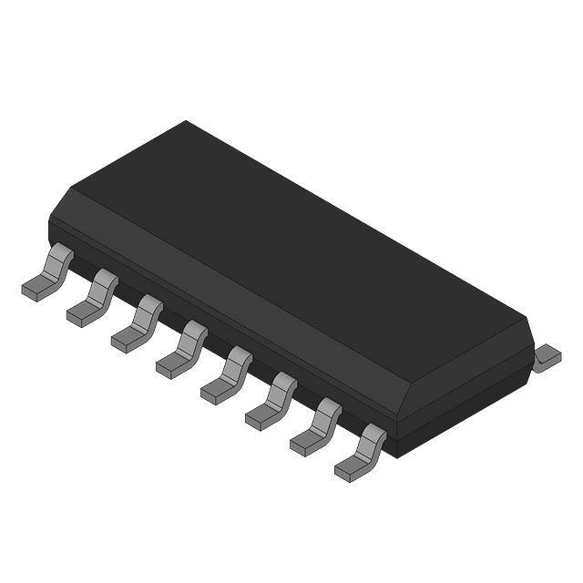
The INA166 is available in a space-saving SO-14
surface-mount package, specified for operation over
the –40°C to +85°C temperature range.
The INA166 is a very low-noise, low-distortion, monolithic instrumentation amplifier. Its current-feedback
circuitry achieves very wide bandwidth and excellent
dynamic response over a wide range of gain. It is ideal
for low-level signals such as microphones or hydrophones. Many industrial, instrumentation, and medical
applications also benefit from its low noise and wide
bandwidth.
VO1
1
INA166
–
VIN
4
3
6kΩ
60kΩ
A1
Sense
8
3kΩ
30.3Ω
A3
9
VO
3kΩ
G = 2000
12
+
VIN
5
6kΩ
A2
Ref
10
14
VO2
Copyright © 2000, Texas Instruments Incorporated
60kΩ
SBOS178
11
V+
6
V–
Printed in U.S.A. December, 2000
�SPECIFICATIONS: VS = ±5V
TA = +25°C and at rated supplies, VS = ±5V, RL = 2kΩ connected to ground, G = 2000, unless otherwise noted.
INA166UA
PARAMETER
CONDITIONS
MIN
GAIN
Gain Error
Gain Temp Drift Coefficient
Nonlinearity
INPUT REFERRED NOISE
Voltage Noise
fO = 1kHz
fO = 100Hz
fO = 10Hz
Current Noise
fO = 1kHz
INPUT OFFSET VOLTAGE
Input Offset Voltage
vs Temperature
vs Power Supply
INPUT VOLTAGE RANGE
Common-Mode Voltage Range
Common-Mode Rejection
TYP
MAX
UNITS
±0.3
±10
±0.005
±1
%
ppm/°C
% of FS
RSOURCE = 0Ω
nV/√Hz
nV/√Hz
nV/√Hz
0.8
pA/√Hz
±50
±2.5
±1
VCM = VOUT = 0V
TA = TMIN to TMAX
VS = ±4.5V to ±18V
+
–
– VIN
= 0V
VIN
+
–
VIN
– VIN
= 0V
VCM = ±1V, RSRC = 0Ω
1.3
1.6
2
(V+) – 4
(V–) + 4
100
INPUT BIAS CURRENT
Initial Bias Current
vs Temperature
Initial Offset Current
vs Temperature
±250
±3
(V+) – 3
(V–) + 3
120
2.5
15
0.1
0.5
µV
µV/°C
µV/V
V
V
dB
12
1
µA
nA/°C
µA
nA/°C
INPUT IMPEDANCE
DYNAMIC RESPONSE
Bandwidth, Small Signal, –3dB
Slew Rate
THD+Noise, f = 1kHz
Settling Time, 0.1%
0.01%
Overload Recovery
OUTPUT
Voltage
Load Capacitance Stability
Short-Circuit Current
POWER SUPPLY
Rated Voltage
Voltage Range
Current, Quiescent
TEMPERATURE RANGE
Specification
Operating
Thermal Resistance, θJA
2
Differential
Common-Mode
60 2
60 2
MΩ pF
MΩ pF
5V Step
5V Step
50% Overdrive
450
15
0.09
2.5
3.5
1
kHz
V/µs
%
µs
µs
µs
(V+) – 1.8
(V–) + 1.8
1000
±60
V
V
pF
mA
RL = 2kΩ to Ground
(V+) – 2
(V–) + 2
Continuous-to-Common
±4.5
IO = 0mA
±5
±10
–40
–40
±18
±12
+85
+125
100
V
V
mA
°C
°C
°C/W
INA166
SBOS178
�ELECTROSTATIC
DISCHARGE SENSITIVITY
PIN CONFIGURATION
Top View
This integrated circuit can be damaged by ESD. Burr-Brown
recommends that all integrated circuits be handled with
appropriate precautions. Failure to observe proper handling
and installation procedures can cause damage.
VO1
1
14 VO2
NC
2
13 NC
GS1
3
12 GS2
–
VIN
4
11 V+
+
VIN
5
10 Ref
V–
6
9
VO
NC
7
8
Sense
ESD damage can range from subtle performance degradation
to complete device failure. Precision integrated circuits may
be more susceptible to damage because very small parametric
changes could cause the device not to meet its published
specifications.
ABSOLUTE MAXIMUM RATINGS(1)
Power Supply Voltage ....................................................................... ±18V
Signal Input Terminals, Voltage(2) .................. (V–) – 0.5V to (V+) + 0.5V
Current(2) .................................................... 10mA
Output Short-Circuit to Ground ............................................... Continuous
Operating Temperature .................................................. –55°C to +125°C
Storage Temperature ..................................................... –55°C to +125°C
Junction Temperature .................................................................... +150°C
Lead Temperature (soldering, 10s) ............................................... +300°C
SO-14
NC = No Internal Connection
NOTES: (1) Stresses above these ratings may cause permanent damage.
Exposure to absolute maximum conditions for extended periods may degrade
device reliability. These are stress ratings only, and functional operation of the
device at these or any other conditions beyond those specified is not implied.
(2) Input terminals are diode-clamped to the power-supply rails. Input signals
that can swing more than 0.5V beyond the supply rails should be current
limited to 10mA or less.
PACKAGE/ORDERING INFORMATION
PRODUCT
PACKAGE
PACKAGE
DRAWING
NUMBER
INA166UA
SO-14 Surface Mount
235
INA166UA
"
"
"
"
PACKAGE
MARKING
ORDERING
NUMBER(1)
TRANSPORT
MEDIA
INA166UA
INA166UA/2K5
Rails
Tape and Reel
NOTE: (1) Models with a slash (/) are available only in Tape and Reel in the quantities indicated (e.g., /2K5 indicates 2500 devices per reel). Ordering 2500 pieces
of “INA166UA/2K5” will get a single 2500-piece Tape and Reel.
INA166
SBOS178
3
�TYPICAL PERFORMANCE CURVES
At TA = +25°C, VS = ±5V, RL = 2kΩ, CL = 50pF, G = 2000, unless otherwise noted.
GAIN vs FREQUENCY
THD+N vs FREQUENCY
70
1
VO = 5Vrms
RL = 10kΩ
60
THD+N (%)
Gain (dB)
50
40
30
0.1
20
10
0
0.01
10k
100k
1M
10M
100
1k
Frequency (Hz)
NOISE VOLTAGE (RTI) vs FREQUENCY
CURRENT NOISE SPECTRAL DENSITY
Current Noise Density (pA/√Hz)
10
1
0.1
1
10
100
1k
10k
1
10
100
10k
POWER-SUPPLY REJECTION
vs FREQUENCY
CMR vs FREQUENCY
140
140
120
120
Power-Supply Rejection (dB)
Input Referred CMR (dB)
1k
Frequency (Hz)
Frequency (Hz)
100
80
60
40
20
100
80
60
40
20
0
0
10
100
1k
10k
Frequency (Hz)
4
100k
10.0
100
Noise (RTI) (nV/√Hz)
10k
Frequency (Hz)
100k
1M
1
10
100
1k
10k
100k
1M
Frequency (Hz)
INA166
SBOS178
�TYPICAL PERFORMANCE CURVES (Cont.)
At TA = +25°C, VS = ±5V, RL = 2kΩ, CL = 50pF, G = 2000, unless otherwise noted.
SMALL-SIGNAL RESPONSE
OUTPUT VOLTAGE SWING vs OUTPUT CURRENT
V+
(V+)–4
500mV/div
Output Voltage to Rail (V)
(V+)–2
(V+)–6
(V–)+6
(V–)+4
(V–)+2
V–
0
10
20
30
40
50
60
2.5µs/div
Output Current (mA)
5V/div
LARGE-SIGNAL RESPONSE
2.5µs/div
INA166
SBOS178
5
�APPLICATIONS INFORMATION
Figure 1 shows the basic connections required for operation.
Power supplies should be bypassed with 0.1µF tantalum capacitors near the device pins. The output Sense (pin 8) and output
Reference (pin 10) should be low-impedance connections. Resistance of greater than 5Ω in series with these connections will
degrade the common-mode rejection of the INA166.
The input stage design used to achieve this low noise, results
in relatively high input bias current and input bias current
noise. As a result, the INA166 may not provide the best
noise performance with a source impedance greater than
10kΩ. For source impedance greater than 10kΩ, other instrumentation amplifiers may provide improved noise performance.
INPUT CONSIDERATIONS
GAIN
Gain of the INA166 is internally set for G = 2000. Input stage
(A1, A2) gain is 200 and the output stage gain (A3) is 10.
Internal resistor values are laser trimmed for accurate ratios to
achieve excellent gain accuracy and common-mode rejection,
but absolute resistor values are approximately ±20%. Nominal
resistor values are shown.
Although the INA166 is primarily intended for fixed-gain
applications, the gain can be increased by connecting a gainset resistor, RG, between pin 3 and pin 12 The nominal gain
will be:
G = 2000 +
Very low source impedance (less than 10Ω) can cause the
INA166 to oscillate. This depends on circuit layout, signal
source, and input cable characteristics. An input network
consisting of a small inductor and resistor, as shown in
Figure 2, can greatly reduce any tendency to oscillate. This
is especially useful if a variety of input sources are to be
connected to the INA166. Although not shown in other
figures, this network can be used as needed with all applications shown.
60000
RG
V+
47Ω
Accuracy of the 60000 term in this equation is approximately ±20%. The stability and temperature drift of RG
contributes to the overall gain accuracy and these effects can
be inferred from this gain equation.
4
3
11
–
VIN
1.2µH
12
5
1.2µH
+
VIN
11
8
9
INA166
VO
10
6
6
47Ω
NOISE PERFORMANCE
V–
The INA166 provides very low-noise with low-source impedance. Its 1.3nV/√Hz voltage noise delivers near-theoretical noise performance with a source impedance of 200Ω.
FIGURE 2. Input Stabilization Network.
V+
0.1µF
1
11
INA166
–
VIN
4
3
6kΩ
60kΩ
A1
Sense
V+
8
Sometimes Shown in
Simplified Form:
3kΩ
30.3Ω
RG
A3
9
VO
3kΩ
INA166
VO
G = 2000
12
+
VIN
5
6kΩ
60kΩ
A2
Ref
10
14
V–
6 0.1µF
NOTE: Gain is internally set to G = 2000.
RG can be used to increase gain. See text.
V–
FIGURE 1. Basic Circuit Connections.
6
INA166
SBOS178
�OFFSET VOLTAGE TRIM
OUTPUT SENSE
A variable voltage applied to pin 10, as shown in Figure 3, can
be used to adjust the output offset voltage. A voltage applied
to pin 10 is summed with the output signal. An op amp
connected as a buffer is used to provide a low impedance at
pin 10 to assure good common-mode rejection.
An output sense terminal allows greater gain accuracy in
driving the load. By connecting the sense connection at the
load, I • R voltage loss to the load is included inside the
feedback loop. Current drive can be increased by connecting
a buffer amp inside the feedback loop, as shown in Figure 4.
V+
4
3
12
5
11
8
V+
9
INA166
VO
10
100µA
6
V–
150Ω
OPA237
10kΩ
150Ω
100µA
V–
FIGURE 3. Offset Voltage Adjustment Circuit.
+15V
Sense
4
3
12
5
±250mA
Output Drive
11
8
9
INA166
10
VO
BUF634
BW
6
BUF634 connected
for wide bandwidth.
–15V
FIGURE 4. Buffer for Increase Output Current.
INA166
SBOS178
7
�PACKAGE OPTION ADDENDUM
www.ti.com
20-Aug-2021
PACKAGING INFORMATION
Orderable Device
Status
(1)
Package Type Package Pins Package
Drawing
Qty
Eco Plan
(2)
Lead finish/
Ball material
MSL Peak Temp
Op Temp (°C)
Device Marking
(3)
(4/5)
(6)
INA166UA
ACTIVE
SOIC
D
14
50
RoHS & Green
NIPDAU
Level-3-260C-168 HR
-55 to 125
INA166UA
INA166UA/2K5
ACTIVE
SOIC
D
14
2500
RoHS & Green
NIPDAU
Level-3-260C-168 HR
-55 to 125
INA166UA
INA166UA/2K5G4
ACTIVE
SOIC
D
14
2500
RoHS & Green
NIPDAU
Level-3-260C-168 HR
-55 to 125
INA166UA
(1)
The marketing status values are defined as follows:
ACTIVE: Product device recommended for new designs.
LIFEBUY: TI has announced that the device will be discontinued, and a lifetime-buy period is in effect.
NRND: Not recommended for new designs. Device is in production to support existing customers, but TI does not recommend using this part in a new design.
PREVIEW: Device has been announced but is not in production. Samples may or may not be available.
OBSOLETE: TI has discontinued the production of the device.
(2)
RoHS: TI defines "RoHS" to mean semiconductor products that are compliant with the current EU RoHS requirements for all 10 RoHS substances, including the requirement that RoHS substance
do not exceed 0.1% by weight in homogeneous materials. Where designed to be soldered at high temperatures, "RoHS" products are suitable for use in specified lead-free processes. TI may
reference these types of products as "Pb-Free".
RoHS Exempt: TI defines "RoHS Exempt" to mean products that contain lead but are compliant with EU RoHS pursuant to a specific EU RoHS exemption.
Green: TI defines "Green" to mean the content of Chlorine (Cl) and Bromine (Br) based flame retardants meet JS709B low halogen requirements of