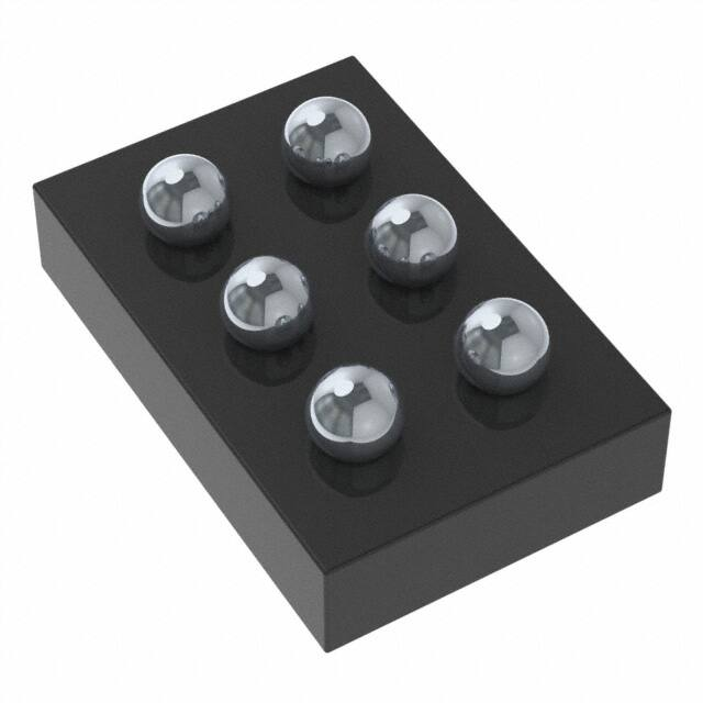
INA191, INA2191
SLYS020C – FEBRUARY 2019 – REVISED AUGUST 2021
INAx191 40-V, Bidirectional, Ultra-Precise Current Sense Amplifier With picoamp IB
and ENABLE in WCSP Package
1 Features
3 Description
•
The INAx191 is a low-power, voltage-output,
current-shunt monitor (also called a current-sense
amplifier) that is commonly used for overcurrent
protection, precision-current measurement for system
optimization, or in closed-loop feedback circuits. This
device can sense drops across shunts at commonmode voltages from –0.2 V to +40 V, independent
of the supply voltage. The low input bias current
of the INAx191 permits the use of larger currentsense resistors, and thus provides accurate current
measurements in the µA range. Five fixed gains
are available: 25 V/V, 50 V/V, 100 V/V, 200 V/V,
or 500 V/V. The low offset voltage of the zero-drift
architecture extends the dynamic range of the current
measurement, and allows for smaller sense resistors
with lower power loss while still providing accurate
current measurements.
•
•
•
•
•
•
Low power:
– Supply voltage, VS: 1.7 V to 5.5 V
– Shutdown current: 100 nA (max INA191)
– Quiescent current: 43 μA at 25 °C (INA191)
Low input bias currents: 100 pA (typical)
(enables microamp current measurement)
Bidirectional current measurement (INA2191)
Accuracy:
– ±0.25% max gain error (A2 to A5 devices)
– 7-ppm/°C gain drift (maximum)
– ±12 μV (maximum) offset voltage
– 0.13-μV/°C offset drift (maximum)
Wide common-mode voltage: –0.2 V to +40 V
Gain options:
– INAx191A1: 25 V/V
– INAx191A2: 50 V/V
– INAx191A3: 100 V/V
– INAx191A4: 200 V/V
– INAx191A5: 500 V/V
Packages:
– INA191: 0.895-mm2 DSBGA
– INA2191: 1.79-mm2 DSBGA
2 Applications
•
•
•
•
•
•
Notebook computers
Cell phones
Battery-powered devices
Telecom equipment
Power management
Battery chargers
Bus Voltage
up to 40 V
100 pA
(typical)
The INA191 operates from a single 1.7-V to 5.5V power supply, drawing a maximum of 65 µA of
supply current when enabled and only 100 nA when
disabled. The device is specified over the operating
temperature range of –40 °C to +125 °C, and offered
in a DSBGA-6 (INA191) and DSBGA-12 (INA2191)
packages.
Device Information(1)
PART NUMBER
PACKAGE
BODY SIZE (NOM)
INA191
DSBGA (6)
1.17 mm × 0.765 mm
INA2191
DSBGA (12)
1.17 mm × 1.53 mm
(1)
For all available packages, see the package option
addendum at the end of the data sheet.
Supply Voltage
1.7 V to 5.5 V
RSENSE
LOAD
0.1 …F
100 pA
(typical)
ENABLE
VS
IN±
INA191
OUT
INA2191 (½)
IN+
ADC
Microcontroller
REF(1)
GND
(1) REF pin only available on INA2191
Simplified Schematic
An IMPORTANT NOTICE at the end of this data sheet addresses availability, warranty, changes, use in safety-critical applications,
intellectual property matters and other important disclaimers. PRODUCTION DATA.
�INA191, INA2191
www.ti.com
SLYS020C – FEBRUARY 2019 – REVISED AUGUST 2021
Table of Contents
1 Features............................................................................1
2 Applications..................................................................... 1
3 Description.......................................................................1
4 Revision History.............................................................. 2
5 Pin Configuration and Functions...................................3
6 Specifications.................................................................. 5
6.1 Absolute Maximum Ratings ....................................... 5
6.2 ESD Ratings .............................................................. 5
6.3 Recommended Operating Conditions ........................5
6.4 Thermal Information ...................................................5
6.5 Electrical Characteristics ............................................6
6.6 Typical Characteristics................................................ 8
7 Detailed Description......................................................15
7.1 Overview................................................................... 15
7.2 Functional Block Diagram......................................... 15
7.3 Feature Description...................................................16
7.4 Device Functional Modes..........................................18
8 Application and Implementation.................................. 22
8.1 Application Information............................................. 22
8.2 Typical Application.................................................... 27
9 Power Supply Recommendations................................28
10 Layout...........................................................................29
10.1 Layout Guidelines................................................... 29
10.2 Layout Examples.................................................... 29
11 Device and Documentation Support..........................31
11.1 Documentation Support.......................................... 31
11.2 Receiving Notification of Documentation Updates.. 31
11.3 Support Resources................................................. 31
11.4 Trademarks............................................................. 31
11.5 Electrostatic Discharge Caution.............................. 31
11.6 Glossary.................................................................. 31
12 Mechanical, Packaging, and Orderable
Information.................................................................... 31
4 Revision History
Changes from Revision B (February 2021) to Revision C (August 2021)
Page
• Changed data sheet status from Production Mixed to Production Data............................................................. 1
• Changed INA2191 device status from Advanced Information to Production Data ............................................ 1
• Added INA191 and INA2191 test conditions to gain error, gain error drift, swing to VS, and enable logic
parameters..........................................................................................................................................................6
• Changed INA191 and INA2191 test conditions for output leakage disabled parameters...................................6
• Changed INA2191 values for the quiescent current parameters for production data.........................................6
• Changed the Typical Characteristics section......................................................................................................8
• Changed INA2191 information in the Low Quiescent Current With Output Enable section............................. 16
• Changed INA2191 information in the Unidirectional Mode section.................................................................. 18
• Changed Figure 8-3 and the filtering information in the Signal Conditioning section....................................... 24
Changes from Revision A (April 2019) to Revision B (February 2021)
Page
• Changed data sheet status from Production Data to Production Mixed............................................................. 1
• Added Advanced Information INA2191 device to the data sheet....................................................................... 1
Changes from Revision * (February 2019) to Revision A (April 2019)
Page
• Changed device from advanced information to production data (active)............................................................1
2
Submit Document Feedback
Copyright © 2021 Texas Instruments Incorporated
Product Folder Links: INA191 INA2191
�INA191, INA2191
www.ti.com
SLYS020C – FEBRUARY 2019 – REVISED AUGUST 2021
5 Pin Configuration and Functions
1
2
3
A
IN+
VS
OUT
B
IN±
GND
ENABLE
Not to scale
Figure 5-1. INA191 YFD Package 6-Pin DSBGA Top View
Table 5-1. Pin Functions (INA191)
PIN
NAME
NO.
TYPE
DESCRIPTION
Enable pin. When this pin is driven to VS, the device is on and functions as a current sense
amplifier. When this pin is driven to GND, the device is off, the supply current is reduced,
and the output is placed in a high-impedance state. This pin must be driven externally, or
connected to VS if not used.
ENABLE
B3
Digital input
GND
B2
Analog
IN+
A1
Analog input
Current-shunt monitor positive input. For high-side applications, connect this pin to the bus
voltage side of the sense resistor. For low-side applications, connect this pin to the load side
of the sense resistor.
IN–
B1
Analog input
Current-shunt monitor negative input. For high-side applications, connect this pin to the load
side of the sense resistor. For low-side applications, connect this pin to the ground side of
the sense resistor.
OUT
A3
Analog output
VS
A2
Analog
Ground.
This pin provides an analog voltage output that is the amplified voltage difference from the
IN+ to the IN– pins.
Power supply, 1.7 V to 5.5 V.
Submit Document Feedback
Copyright © 2021 Texas Instruments Incorporated
Product Folder Links: INA191 INA2191
3
�INA191, INA2191
www.ti.com
SLYS020C – FEBRUARY 2019 – REVISED AUGUST 2021
1
2
3
A
IN+1
VS
OUT1
B
IN-1
EN1
REF1
C
IN-2
EN2
REF2
D
IN+2
GND
OUT2
Figure 5-2. INA2191 YBJ Package 12-Pin DSBGA Top View
Table 5-2. Pin Functions (INA2191)
PIN
4
TYPE
DESCRIPTION
B2
Digital input
Enable pin for output 1. When this pin is driven to VS, channel 1 is on and functions as a
current sense amplifier. When both enable pins are driven to GND, the device is off and the
supply current is reduced. This pin must be driven externally, or connected to VS if not used.
ENABLE2
C2
Digital input
Enable pin for output 2. When this pin is driven to VS, channel 2 is on and functions as a
current sense amplifier. When both enable pins are driven to GND, the device is off and the
supply current is reduced. This pin must be driven externally, or connected to VS if not used.
GND
D2
Analog
IN+1
A1
Analog input
Current-shunt monitor positive input for channel 1. For high-side applications, connect this
pin to the bus voltage side of the sense resistor. For low-side applications, connect this pin
to the load side of the sense resistor.
IN+2
D1
Analog input
Current-shunt monitor positive input for channel 2. For high-side applications, connect this
pin to the bus voltage side of the sense resistor. For low-side applications, connect this pin
to the load side of the sense resistor.
IN–1
B1
Analog input
Current-shunt monitor negative input for channel 1. For high-side applications, connect this
pin to the load side of the sense resistor. For low-side applications, connect this pin to the
ground side of the sense resistor.
IN–2
C1
Analog input
Current-shunt monitor negative input for channel 2. For high-side applications, connect this
pin to the load side of the sense resistor. For low-side applications, connect this pin to the
ground side of the sense resistor.
OUT1
A3
Analog output
This pin provides an analog voltage output that is the amplified voltage difference from the
IN+1 to the IN–1 pins, and is offset by the voltage applied to the REF1 pin.
OUT2
D3
Analog output
This pin provides an analog voltage output that is the amplified voltage difference from the
IN+2 to the IN–2 pins, and is offset by the voltage applied to the REF2 pin.
REF1
B3
Analog input
Reference input for channel 1. Enables bidirectional current sensing for channel 1 with an
externally applied voltage.
REF2
C3
Analog input
Reference input for channel 2. Enables bidirectional current sensing for channel 2 with an
externally applied voltage.
VS
A2
Analog
NAME
NO.
ENABLE1
Ground.
Power supply, 1.7 V to 5.5 V.
Submit Document Feedback
Copyright © 2021 Texas Instruments Incorporated
Product Folder Links: INA191 INA2191
�INA191, INA2191
www.ti.com
SLYS020C – FEBRUARY 2019 – REVISED AUGUST 2021
6 Specifications
6.1 Absolute Maximum Ratings
over operating free-air temperature range (unless otherwise noted)(1)
MIN
VS
MAX
Supply voltage
)(2)
Differential (VIN+) – (VIN–
VIN+, VIN– Analog inputs
VENABLE
VIN+, VIN–, with respect to GND(3)
–42
42
GND – 0.3
42
ENABLE
GND – 0.3
6
REF, OUT(3)
GND – 0.3
(VS) + 0.3
Input current into any pin(3)
TA
Operating temperature
TJ
Junction temperature
Tstg
Storage temperature
(1)
(2)
(3)
UNIT
6
–55
–65
V
V
V
V
5
mA
150
°C
150
°C
150
°C
Stresses beyond those listed under Absolute Maximum Ratings may cause permanent damage to the device. These are stress
ratings only, which do not imply functional operation of the device at these or any other conditions beyond those indicated under
Recommended Operating Conditions. Exposure to absolute-maximum-rated conditions for extended periods may affect device
reliability.
VIN+ and VIN– are the voltages at the IN+ and IN– pins, respectively.
Input voltage at any pin may exceed the voltage shown if the current at that pin is limited to 5 mA.
6.2 ESD Ratings
VALUE
V(ESD)
(1)
(2)
Electrostatic discharge
Human-body model (HBM), per ANSI/ESDA/JEDEC JS-001(1)
±2000
Charged-device model (CDM), per JEDEC specification JESD22-C101(2)
±1000
UNIT
V
JEDEC document JEP155 states that 500-V HBM allows safe manufacturing with a standard ESD control process.
JEDEC document JEP157 states that 250-V CDM allows safe manufacturing with a standard ESD control process.
6.3 Recommended Operating Conditions
over operating free-air temperature range (unless otherwise noted)
MIN
NOM
MAX
UNIT
VCM
Common-mode input range
– 0.2
40
V
VIN+, VIN–
Input pin voltage range
– 0.2
40
V
VS
Operating supply voltage
1.7
5.5
V
VREF
Reference pin voltage range
0
VS
V
TA
Operating free-air temperature
–40
125
°C
6.4 Thermal Information
THERMAL
METRIC(1)
INA191
INA2191
YFD (DSBGA)
YBJ (DSBGA)
6 PINS
12 PINS
141.4
94.1
°C/W
UNIT
RθJA
Junction-to-ambient thermal resistance
RθJC(top)
Junction-to-case (top) thermal resistance
1.1
0.6
°C/W
RθJB
Junction-to-board thermal resistance
45.7
23.8
°C/W
ΨJT
Junction-to-top characterization parameter
0.4
0.3
°C/W
ΨJB
Junction-to-board characterization parameter
45.3
23.8
°C/W
RθJC(bot)
Junction-to-case (bottom) thermal resistance
N/A
N/A
°C/W
(1)
For more information about traditional and new thermal metrics, see the Semiconductor and IC Package Thermal Metrics application
report.
Submit Document Feedback
Copyright © 2021 Texas Instruments Incorporated
Product Folder Links: INA191 INA2191
5
�INA191, INA2191
www.ti.com
SLYS020C – FEBRUARY 2019 – REVISED AUGUST 2021
6.5 Electrical Characteristics
at TA = 25°C, VSENSE = VIN+ – VIN–, VS = 1.8 V to 5.0 V, VIN+ = 12 V, VREF = VS / 2 (INA2191), and VENABLE = VS (unless
otherwise noted)
PARAMETER
CONDITIONS
MIN
TYP
132
150
MAX
UNIT
INPUT
CMRR
Common-mode
rejection ratio, RTI(1)
RTI(1)
VIN+ = –0.1 V to 40 V, TA = –40°C to +125°C
VOS
Offset voltage,
dVOS/dT
Offset drift, RTI
VS = 1.8 V
PSRR
Power-supply rejection
VS = 1.7 V to 5.5 V
ratio, RTI
IIB
Input bias current
IIO
Input offset current
dB
–2.5
±12
µV
10
130
nV/°C
–1
±5
µV/V
VSENSE = 0 mV
0.1
3
nA
VSENSE = 0 mV
±0.07
TA = –40°C to +125°C
nA
OUTPUT
G
Gain
A1 devices
25
A2 devices
50
A3 devices
100
A4 devices
200
A5 devices
EG
RVRR
Gain error
500
VOUT = 0.1 V to VS – 0.1 V
Gain error drift
TA = –40°C to +125°C
Nonlinearity error
VOUT = 0.1 V to VS – 0.1 V
Reference voltage
rejection ratio
INA2191 only,
VREF = 100 mV to VS – 100 mV,
TA = –40°C to +125°C
A1 devices, INA191
–0.17%
±0.35%
A1 devices, INA2191
+0.05%
±0.25%
A2, A3, A4, A5
devices
–0.04%
±0.25%
2
7
ppm/°C
±0.01%
A1 devices
±2
±12
A2 devices
±1
±6
A3 devices
±0.5
±4
±0.25
±3
A4, A5 devices
Maximum capacitive
load
V/V
No sustained oscillation
1
µV/V
nF
VOLTAGE OUTPUT
VSP
Swing to VS powersupply rail
VS = 1.8 V, RL = 10 kΩ to GND, TA = –40°C to +125°C
(VS) – 23
(VS) – 40
mV
VSN
Swing to GND
VS = 1.8 V, RL = 10 kΩ to GND, TA = –40°C to +125°C,
VSENSE = –10 mV, VREF = 0 V (INA2191)
(VGND) + 0.05
(VGND) + 1
mV
A1, A2, A3 devices
VS = 1.8 V, RL = 10 kΩ to GND,
TA = –40°C to +125°C, VSENSE = 0 mV, A4 devices
for INA2191 VREF = 0 V
A5 devices
(VGND) + 3
mV
Zero current output
voltage
(VGND) + 1
VZL
(VGND) + 2
(VGND) + 4
mV
(VGND) + 3
(VGND) + 7
mV
FREQUENCY RESPONSE
BW
Bandwidth
CLOAD = 10 pF
A1 devices
45
A2 devices
37
A3 devices
35
A4 devices
33
A5 devices
6
kHz
27
SR
Slew rate
VS = 5.0 V, VOUT = 0.5 V to 4.5 V
0.3
V/µs
tS
Settling time
From current step to within 1% of final value
30
µs
Submit Document Feedback
Copyright © 2021 Texas Instruments Incorporated
Product Folder Links: INA191 INA2191
�INA191, INA2191
www.ti.com
SLYS020C – FEBRUARY 2019 – REVISED AUGUST 2021
at TA = 25°C, VSENSE = VIN+ – VIN–, VS = 1.8 V to 5.0 V, VIN+ = 12 V, VREF = VS / 2 (INA2191), and VENABLE = VS (unless
otherwise noted)
PARAMETER
CONDITIONS
MIN
TYP
MAX
UNIT
NOISE, RTI(1)
Voltage noise density
75
nV/√Hz
ENABLE
IEN
Leakage input current
100
nA
VIH
High-level input voltage TA = –40°C to +125°C
1.35
5.5
V
VIL
Low-level input voltage TA = –40°C to +125°C
0
0.4
VHYS
Hysteresis
IODIS
0 V ≤ VENABLE ≤ VS
1
100
V
mV
Output leakage
disabled
VS = 1.8 V, VOUT = 0 V to 1.8 V, VENABLE = 0 V
1
5
µA
Output leakage
disabled (INA2191)
VS = 5 V, VOUT = 0 V to 5.0 V, VENABLE = 0 V
1
5
µA
43
65
µA
85
µA
130
µA
180
µA
POWER SUPPLY
IQ
Quiescent current
(INA191)
VS = 1.8 V, VSENSE = 0 mV
Quiescent current
(INA2191)
VS = 1.8 V, VSENSE = 0 mV (Dual Channel)
VS = 1.8 V, VSENSE = 0 mV, TA = –40°C to +125°C
96
VS = 1.8 V, VSENSE = 0 mV, TA = –40°C to +125°C
IQDIS
Quiescent current
disabled (INA191)
VENABLE < 0.4 V, VSENSE = 0 mV (Single Channel)
10
100
nA
IQDIS
Quiescent current
disabled (INA2191)
VENABLE1 < 0.4 V, VENABLE2 = < 0.4 V, VSENSE = 0 mV
20
200
nA
(1)
RTI = referred-to-input.
Submit Document Feedback
Copyright © 2021 Texas Instruments Incorporated
Product Folder Links: INA191 INA2191
7
�INA191, INA2191
www.ti.com
SLYS020C – FEBRUARY 2019 – REVISED AUGUST 2021
6.6 Typical Characteristics
at TA = 25 °C, VS = 1.8 V, VIN+ = 12 V, VENABLE = VS, VREF = GND and all gain options (unless otherwise noted)
15
Population
Offset Voltage (PV)
10
5
0
-5
-12
-10.8
-9.6
-8.4
-7.2
-6
-4.8
-3.6
-2.4
-1.2
0
1.2
2.4
3.6
4.8
6
7.2
8.4
9.6
10.8
12
-10
Input Offset Voltage (PV)
-15
-50
D118
Figure 6-1. Input Offset Voltage Production
Distribution
25
50
75
Temperature (qC)
100
125
150
D006
0.1
Common-Mode Rejection Ratio (PV/V)
30000
27000
24000
21000
18000
15000
12000
9000
6000
3000
-0.25
-0.225
-0.2
-0.175
-0.15
-0.125
-0.1
-0.075
-0.05
-0.025
0
0.025
0.05
0.075
0.1
0.125
0.15
0.175
0.2
0.225
0.25
0
D119
0.08
0.06
0.04
0.02
0
-0.02
-0.04
-0.06
-0.08
-0.1
-50
-25
Common-Mode Rejection Ratio (PV/V)
0
25
50
75
Temperature (qC)
100
125
150
D012
Figure 6-4. Common-Mode Rejection Ratio vs.
Temperature
D116
-0.25
-0.225
-0.2
-0.175
-0.15
-0.125
-0.1
-0.075
-0.05
-0.025
0
0.025
0.05
0.075
0.1
0.125
0.15
0.175
0.2
0.225
0.25
-0.35
-0.33
-0.31
-0.29
-0.27
-0.25
-0.23
-0.21
-0.19
-0.17
-0.15
-0.13
-0.11
-0.09
-0.07
-0.05
-0.03
-0.01
0.01
0.03
0.05
Population
Population
Figure 6-3. Common-Mode Rejection Production
Distribution
Gain Error (%)
Gain Error (%)
A1 Devices
A1 devices
Figure 6-5. Gain Error Production Distribution
(INA191)
8
0
Figure 6-2. Offset Voltage vs. Temperature
33000
Population
-25
Figure 6-6. Gain Error Production Distribution
(INA2191)
Submit Document Feedback
Copyright © 2021 Texas Instruments Incorporated
Product Folder Links: INA191 INA2191
�INA191, INA2191
www.ti.com
SLYS020C – FEBRUARY 2019 – REVISED AUGUST 2021
0.2
0.16
0.12
Population
Gain Error (%)
0.08
0.04
0
-0.04
-0.08
-0.12
-0.25
-0.225
-0.2
-0.175
-0.15
-0.125
-0.1
-0.075
-0.05
-0.025
0
0.025
0.05
0.075
0.1
0.125
0.15
0.175
0.2
0.225
0.25
-0.16
-0.2
-50
-25
0
25
50
75
Temperature (qC)
D117
100
125
150
D018
Gain Error (%)
Figure 6-8. Gain Error vs. Temperature
A2, A3, A4, A5 devices
Figure 6-7. Gain Error Production Distribution
60
140
Power-Supply Rejection Ratio (dB)
50
Gain (dB)
40
30
20
10
0
-10
-20
10
A1
A2
A3
A4
A5
100
1k
10k
Frequency (Hz)
100k
120
100
80
60
40
20
0
10
1M
100
1k
10k
Frequency (Hz)
D019
VS = 5 V
1M
D020
VS = 5 V
Figure 6-9. Gain vs. Frequency
Figure 6-10. Power-Supply Rejection Ratio vs.
Frequency
Vs
160
140
-40°C
25°C
125°C
Vs-0.4
120
100
80
Vs-0.8
Y
Output Swing (V)
Common-Mode Rejection Ratio (dB)
100k
GND+0.8
GND+0.4
60
GND
40
10
0
100
1k
10k
Frequency (Hz)
100k
1
1M
3
4
5
6
7
Output Current (mA)
8
9
10
11
D010
VS = 1.8 V
D021
Figure 6-11. Common-Mode Rejection Ratio vs.
Frequency
2
Figure 6-12. Output Voltage Swing vs. Output
Current
Submit Document Feedback
Copyright © 2021 Texas Instruments Incorporated
Product Folder Links: INA191 INA2191
9
�INA191, INA2191
www.ti.com
SLYS020C – FEBRUARY 2019 – REVISED AUGUST 2021
Vs
0.2
0.15
Input Bias Current (nA)
Vs-1
Vs-2
Y
Output Swing (V)
0.25
-40°C
25°C
125°C
GND+2
GND+1
0.1
0.05
0
-0.05
-0.1
-0.15
-0.2
GND
0
5
10
15
20
25
Output Current (mA)
30
35
-0.25
0
D009
5
10
VS = 5.0 V
Figure 6-13. Output Voltage Swing vs. Output
Current
0.2
6
Input Bias Current (nA)
Input Bias Current (nA)
0.15
0
-0.05
-0.1
-0.15
D024
5
4
3
2
1
0
-0.2
-0.25
0
5
10
15
20
25
30
Common-Mode Voltage (V)
35
-1
-50
40
-25
0
D025
VENABLE = 0 V, VSENSE = 0 V
125
150
D026
90
VS = 1.8V
VS = 3.3V
VS = 5V
80
Quiescent Current (PA)
60
100
Figure 6-16. Input Bias Current vs. Temperature
70
65
25
50
75
Temperature (qC)
VSENSE = 0 V
Figure 6-15. Input Bias Current vs. Common-Mode
Voltage (Shutdown)
Quiescent Current (PA)
40
Figure 6-14. Input Bias Current vs. Common-Mode
Voltage
7
0.05
35
VS = 5.0 V, VSENSE = 0 V
0.25
0.1
15
20
25
30
Common-Mode Voltage (V)
55
50
45
40
35
VS = 1.8V
VS = 3.3V
VS = 5V
70
60
50
40
30
25
-50
30
-50
-25
0
25
50
75
Temperature (qC)
100
125
D101
VENABLE = VS
Figure 6-17. Quiescent Current vs. Temperature
(INA191)
10
-25
150
0
25
50
75
Temperature (qC)
100
125
150
Single channel enabled, VREF = VS /2
Figure 6-18. Quiescent Current vs. Temperature
(INA2191 )
Submit Document Feedback
Copyright © 2021 Texas Instruments Incorporated
Product Folder Links: INA191 INA2191
�INA191, INA2191
www.ti.com
SLYS020C – FEBRUARY 2019 – REVISED AUGUST 2021
240
160
Quiescent Current (PA)
140
VS = 1.8V
VS = 3.3V
VS = 5V
210
180
Quiescent Current (nA)
150
130
120
110
100
90
80
150
120
90
60
30
70
60
-50
VS = 1.8 V
VS = 3.3 V
VS = 5.0 V
0
-25
0
25
50
75
Temperature (qC)
100
125
-30
-50
150
-25
0
25
50
75
Temperature (qC)
VENABLE1 = VENABLE2 = VS
, VREF = VS /2
Quiescent Current (PA)
Quiescent Current (PA)
VS = 1.8V
VS = 5V
55
200
150
100
50
0
50
45
40
35
-25
0
25
50
75
Temperature (qC)
100
125
30
-5
150
0
VENABLE1 = VENABLE2 = 0 V, VREF = VS /2
Figure 6-21. Quiescent Current vs. Temperature
(INA2191 Disabled)
5
10
15
20
25
30
Common-Mode Voltage (V)
35
40
D103
Figure 6-22. Quiescent Current vs. Common-Mode
Voltage (INA191)
120
110
105
100
95
0
5
10
15
20
25
Common-Mode Voltage (V)
30
35
40
VREF = VS /2
Figure 6-23. Quiescent Current vs. Common-Mode
Voltage (INA2191)
Input-Referred Voltage Noise (nV/—Hz)
500
VS = 1.8V
VS = 5V
115
Quiescent Current (PA)
D002
60
VS = 1.8V
VS = 3.3V
VS = 5V
250
90
-5
150
Figure 6-20. Quiescent Current vs. Temperature
(INA191 Disabled)
350
-50
-50
125
VENABLE = 0 V
Figure 6-19. Quiescent Current vs. Temperature
(INA2191 )
300
100
300
200
100
70
50
30
20
10
10
100
1k
Frequency (Hz)
10k
100k
Figure 6-24. Input-Referred Voltage Noise vs.
Frequency
Submit Document Feedback
Copyright © 2021 Texas Instruments Incorporated
Product Folder Links: INA191 INA2191
11
�INA191, INA2191
www.ti.com
Input Voltage
5 mV/div
Referred-to-Input
Voltage Noise (0.5 PV/div)
Output Voltage
500 mV/div
SLYS020C – FEBRUARY 2019 – REVISED AUGUST 2021
0V
0V
Time (20Ps/div)
Time (1 s/div)
D111
D031
VS = 5.0 V, 10-mVPP input step
Figure 6-25. 0.1-Hz to 10-Hz Input-Referred Voltage
Noise
Figure 6-26. Step Response
Inverting Input
Output
VCM
VOUT
50
40
20
10
0
-10
-20
Voltage (1 V/div)
30
VOUT (250 mV/div)
Common-Mode Voltage (10 V/div)
60
-30
-40
0V
-50
-60
Time (500 Ps/div)
Time (20 Ps/div)
D114
Figure 6-27. Common-Mode Voltage Transient
Response
Figure 6-28. Inverting Differential Input Overload
Recovery
Voltage (1V/div)
Supply Voltage
Output Voltage
Voltage (1 V/div)
Noninverting Input
Output
0V
0V
Time (20 Ps/div)
Time (10Ps/div)
D113
D108
VS = 5.0 V
VS = 5.0 V, A2 device
Figure 6-29. Noninverting Differential Input
Overload Recovery
12
Figure 6-30. Start-Up Response
Submit Document Feedback
Copyright © 2021 Texas Instruments Incorporated
Product Folder Links: INA191 INA2191
�INA191, INA2191
www.ti.com
SLYS020C – FEBRUARY 2019 – REVISED AUGUST 2021
Enable
Output
Voltage (1 V/div)
Voltage (1 V/div)
Supply Voltage
Output Voltage
0V
0V
Time (250 Ps/div)
Time (100Ps/div)
D021
D110
VS = 5.0 V, A3 device
VS = 5.0 V, A3 device
Figure 6-32. Enable and Disable Response
Figure 6-31. Brownout Recovery
30
120
IBN
IBP
100
20
60
Input Bias Current (nA)
Input Bias Current (nA)
80
IBP
IBN
40
20
0
-20
-40
-60
-80
10
0
-10
-20
-100
-120
-30
0
20
40
60
80 100 120 140 160
Differential Input Voltage (mV)
180
200
0
5
VS = 5.0 V, A1 device
15 20 25 30 35 40
Differential Input Voltage (mV)
45
50
55
D007
VS = 5.0 V, A2, A3, A4, A5 devices
Figure 6-33. IB+ and IB– vs. Differential Input
Voltage (INA191)
Figure 6-34. IB+ and IB– vs. Differential Input
Voltage (INA191)
120
35
IBN
IBP
100
60
40
20
0
-20
-40
-60
IBN
IBP
25
Input Bias Current (nA)
80
Input Bias Current (nA)
10
D120
15
5
-5
-15
-25
-80
-100
-120
-110 -90
-70
-50 -30 -10 10 30 50
Differential Input Voltage (mV)
70
90
110
-35
-60
-40
-20
0
20
Differential Input Voltage (mV)
40
60
VS = 5.0 V, VREF = VS /2, A2, A3, A4, A5 devices
VS = 5.0 V, VREF = VS /2, A1 device
Figure 6-35. IB+ and IB– vs. Differential Input
Voltage (INA2191)
Figure 6-36. IB+ and IB– vs. Differential Input
Voltage (INA2191)
Submit Document Feedback
Copyright © 2021 Texas Instruments Incorporated
Product Folder Links: INA191 INA2191
13
�INA191, INA2191
www.ti.com
SLYS020C – FEBRUARY 2019 – REVISED AUGUST 2021
5.5
2.75
-40qC
25qC
125qC
2.25
-40qC
25qC
125qC
5
Output Leakage Current (PA)
Output Leakage Current (PA)
2.5
2
1.75
1.5
1.25
1
0.75
0.5
4.5
4
3.5
3
2.5
2
1.5
1
0.5
0.25
0
0
0
0.5
1
1.5
2
2.5
3
3.5
Output Voltage (V)
4
4.5
0
5
2
2.5
3
3.5
Output Voltage (V)
4
4.5
5
D107
Figure 6-38. Output Leakage vs. Output Voltage
1.25
3
-40qC
25qC
125qC
0.75
25qC
-40qC
125qC
2.5
Output Leakage Current (PA)
1
Output Leakage Current (PA)
1.5
VS = 5.0 V, VENABLE = 0 V, A4, A5 devices
Figure 6-37. Output Leakage vs. Output Voltage
0.5
0.25
0
-0.25
-0.5
-0.75
2
1.5
1
0.5
0
-0.5
-1
-1.5
-2
-1
0
0.5
1
1.5
2
2.5
3
3.5
Output Voltage (V)
4
4.5
-2.5
5
0
1
1.5
2
2.5
3
3.5
Output Voltage (V)
4
4.5
5
D048
VS = 5.0 V, VENABLE = 0 V, VREF = 2.5 V, A4, A5 devices
Figure 6-39. Output Leakage vs. Output Voltage
(INA2191)
Figure 6-40. Output Leakage vs. Output Voltage
(INA2191)
160
5000
A4
A3
100
10
A1
1
100
1k
A2
10k
100k
Frequency (Hz)
Gain Variants
A1
A2
A3
A4
A5
1M
VS = 5.0 V, VCM = 0 V
10M
Channel Separation (dB)
A5
1000
0.1
10
0.5
D040
VS = 5.0 V, VENABLE = 0 V, VREF = 2.5 V, A1, A2, A3 devices
Output Impedance (:)
1
D105
VS = 5.0 V, VENABLE = 0 V, A1, A2, A3 devices
140
120
100
80
60
10
100
1k
Frequency (Hz)
10k
100k
VS = 5.0 V, VCM = 0 V, VREF = VS /2
Figure 6-41. Output Impedance vs. Frequency
14
0.5
Figure 6-42. Channel Separation vs. Frequency
(INA2191)
Submit Document Feedback
Copyright © 2021 Texas Instruments Incorporated
Product Folder Links: INA191 INA2191
�INA191, INA2191
www.ti.com
SLYS020C – FEBRUARY 2019 – REVISED AUGUST 2021
7 Detailed Description
7.1 Overview
The INAx191 is a low bias current, 40-V common-mode, current-sensing amplifier with an enable pin. When
disabled, the output goes to a high-impedance state, and the supply current draw is reduced to less than 0.1
µA per channel. The INAx191 is intended for use in either low-side and high-side current-sensing configurations
where high accuracy and low current consumption are required. The INAx191 is a specially designed currentsensing amplifier, that accurately measure voltages developed across current-sensing resistors on commonmode voltages that far exceed the supply voltage. Current can be measured on input voltage rails as high as 40
V, with a supply voltage (VS) as low as 1.7 V.
7.2 Functional Block Diagram
VS
ENABLE
INA191
IN+
+
±
±
+
±
OUT
+
IN±
GND
Figure 7-1. INA191 Diagram
VS
INA2191
ENABLE1
IN+1
+
±
±
±
+
+
OUT1
IN±1
REF1
ENABLE2
IN+2
+
±
±
+
±
OUT2
+
IN±2
REF2
GND
Figure 7-2. INA2191 Diagram
Submit Document Feedback
Copyright © 2021 Texas Instruments Incorporated
Product Folder Links: INA191 INA2191
15
�INA191, INA2191
SLYS020C – FEBRUARY 2019 – REVISED AUGUST 2021
www.ti.com
7.3 Feature Description
7.3.1 Precision Current Measurement
The INAx191 provides accurate current measurements over a wide dynamic range. The high accuracy of the
device is attributable to the low gain error and offset specifications. The offset voltage of the INAx191 is less than
12 µV. In this case, the low offset improves the accuracy at light loads when VIN+ approaches VIN–.
Another advantage of low offset is the ability to use a lower-value shunt resistor that reduces the power loss in
the current-sense circuit, and improves the power efficiency of the end application.
The maximum gain error of the INAx191 is specified to be within 0.25% for most gain options. As the sensed
voltage becomes much larger than the offset voltage, the gain error becomes the dominant source of error in
the current-sense measurement. When the device monitors currents near the full-scale output range, the total
measurement error approaches the value of the gain error.
7.3.2 Low Input Bias Current
The INAx191 is different from many current-sense amplifiers because this device offers very low input bias
current. The low input bias current of the INAx191 has three primary benefits.
The first benefit is the reduction of the current consumed by the device in both the enabled and disabled states.
Classical current-sense amplifier topologies typically consume tens of microamps of current at the inputs. For
these amplifiers, the input current is the result of the resistor network that sets the gain and additional current
to bias the input amplifier. To reduce the bias current to near zero, the INAx191 uses a capacitively coupled
amplifier on the input stage, followed by a difference amplifier on the output stage.
The second benefit of low bias current is the ability to use input filters to reject high-frequency noise before
the signal is amplified. In a traditional current-sense amplifier, the addition of input filters comes at the cost
of reduced accuracy. However, as a result of the low bias currents, input filters have little effect on the
measurement accuracy of the INAx191.
The third benefit of low bias current is the ability to use a larger current-sense resistor. This ability allows the
device to accurately monitor currents as low as 1 µA.
7.3.3 Low Quiescent Current With Output Enable
The device features low quiescent current (IQ), while still providing sufficient small-signal bandwidth to be usable
in most applications. The quiescent current of the INA191 is only 43 µA (typical), while providing a small-signal
bandwidth of 35 kHz in a gain of 100. The low IQ and good bandwidth allow the device to be used in many
portable electronic systems without excessive drain on the battery. Because many applications only need to
periodically monitor current, the INAx191 features an enable pin for each output that turns off the device until
needed. When in the disabled state, the INAx191 typically draws 10 nA of total supply current per channel.
7.3.4 Bidirectional Current Monitoring (INA2191 Only)
The INA2191 can sense current flow through a sense resistor in both directions. The bidirectional currentsensing capability is achieved by applying a voltage at the REF pin to offset the desired output voltage. A
positive differential voltage sensed at the inputs results in an output voltage that is greater than the applied
reference voltage. Likewise, a negative differential voltage at the inputs results in output voltage that is less than
the applied reference voltage. The output voltage of the current-sense amplifier is shown in Equation 1. Equation
variables such as VOUT are valid for either VOUT1 or VOUT2 depending on which channel used.
VOUT
I LOAD u RSENSE u GAIN
VREF
(1)
where
•
•
•
•
16
ILOAD is the load current to be monitored.
RSENSE is the current-sense resistor.
GAIN is the gain option of the selected device.
VREF is the voltage applied to the REF pin.
Submit Document Feedback
Copyright © 2021 Texas Instruments Incorporated
Product Folder Links: INA191 INA2191
�INA191, INA2191
www.ti.com
SLYS020C – FEBRUARY 2019 – REVISED AUGUST 2021
7.3.5 High-Side and Low-Side Current Sensing
The INAx191 supports input common-mode voltages from –0.2 V to +40 V. Because of the internal topology,
the common-mode range is not restricted by the power-supply voltage (VS). The ability to operate with commonmode voltages greater or less than VS allows the INAx191 to be used in high-side and low-side current-sensing
applications, as shown in Figure 7-3.
Bus Suppl y
up to +40 V
IN+
R SENS E
High-Side Se nsing
Commo n-mode volta ge (VCM )
is b us-voltage depen dent.
IN±
LOA D
IN+
R SENS E
Low-Side Se nsing
Commo n-mode volta ge (VCM )
is a lwa ys n ear groun d a nd is
isolated fro m bus-voltage sp ikes.
IN±
Figure 7-3. High-Side and Low-Side Sensing Connections
7.3.6 High Common-Mode Rejection
The INAx191 uses a capacitively coupled amplifier on the front end. Therefore, dc common-mode voltages are
blocked from downstream circuits, resulting in very high common-mode rejection. The common-mode rejection
of the INAx191 is 150 dB (typical). The ability to reject changes in the DC common-mode voltage allows the
INAx191 to monitor both high- and low-voltage rail currents with very little change in the offset voltage.
7.3.7 Rail-to-Rail Output Swing
The INAx191 supports linear current-sensing operation with the output close to the supply rail and ground. The
maximum specified output swing to the positive rail is VS – 40 mV, and the maximum specified output swing
to GND is only GND + 1 mV with –10 mV of differential overdrive. For cases where the sense current is zero,
the swing to ground is determined by the zero current output specification. The value of the zero current output
voltage can differ from the specified value depending on the common-mode voltage, supply voltage, and output
load. The close-to-rail output swing maximizes the usable output range, particularly when operating the device
from a 1.8-V supply.
Submit Document Feedback
Copyright © 2021 Texas Instruments Incorporated
Product Folder Links: INA191 INA2191
17
�INA191, INA2191
www.ti.com
SLYS020C – FEBRUARY 2019 – REVISED AUGUST 2021
7.4 Device Functional Modes
7.4.1 Normal Operation
The INAx191 is in normal operation when the following conditions are met:
•
•
•
•
•
The power-supply voltage (VS) is between 1.7 V and 5.5 V.
The common-mode voltage (VCM) is within the specified range of –0.2 V to +40 V.
The maximum differential input signal times the gain plus VREF is less than the positive output voltage swing
VSP. VREF = 0 V for INA191.
The ENABLE pin is driven or connected to VS.
The minimum differential input signal times the gain plus VREF is greater than the swing to GND, VZL (see
Section 7.3.7). VREF = 0 V for INA191.
During normal operation, this device produces an output voltage that is the amplified representation of the
difference voltage from IN+ to IN– plus the voltage applied to the REF pin. For devices without a REF pin the
REF voltage is 0 V.
7.4.2 Unidirectional Mode
The INA191 always monitors current flow in a single direction, however, the INA2191 can be configured to
monitor current flowing in one direction (unidirectional) or in both directions (bidirectional) depending on how
the REF pin is connected. The most common case is unidirectional where the output is set to ground when no
current is flowing by connecting the REF pin to ground, as shown in Figure 7-4. When the current flows from the
bus supply to the load, the input voltage from IN+ to IN– increases and causes the output voltage at the OUT pin
to increase. Pin names such as OUT apply to either OUT1 or OUT2 in the diagrams below depending on which
channel is used.
Bus Voltage
up to 40 V
RSENSE
VS
1.7 V to 5.5 V
Load
CBYPASS
0.1 µF
ISENSE
ENABLE
VS
INA2191 (½)
IN±
Capacitively
Coupled
Amplifier
±
OUT
VOUT
+
REF
IN+
GND
Figure 7-4. Typical Unidirectional Application
The linear range of the output stage is limited by how close the output voltage can approach ground under
zero input conditions. The zero current output voltage of the INA2191 is very small and for most unidirectional
applications the REF pin is simply grounded. However, if the measured current multiplied by the current sense
resistor and device gain is less than the zero current output voltage then bias the REF pin to a convenient value
above the zero current output voltage to get the output into the linear range of the device. To limit reference
rejection errors, buffer the reference voltage connected to the REF pin.
A less-frequently used output biasing method is to connect the REF pin to the power-supply voltage, VS. This
method results in the output voltage saturating at 40 mV less than the supply voltage when no differential input
voltage is present. This method is similar to the output saturated low condition with no differential input voltage
18
Submit Document Feedback
Copyright © 2021 Texas Instruments Incorporated
Product Folder Links: INA191 INA2191
�INA191, INA2191
www.ti.com
SLYS020C – FEBRUARY 2019 – REVISED AUGUST 2021
when the REF pin is connected to ground. The output voltage in this configuration only responds to currents
that develop negative differential input voltage relative to the device IN– pin. Under these conditions, when
the negative differential input signal increases, the output voltage moves downward from the saturated supply
voltage. The voltage applied to the REF pin must not exceed VS.
Another use for the REF pin in unidirectional operation is to level shift the output voltage. Figure 7-5 shows an
application where the device ground is set to a negative voltage so currents biased to negative supplies, as seen
in optical networking cards, can be measured. The GND of the INA2191 can be set to negative voltages, as
long as the inputs do not violate the common-mode range specification and the voltage difference between VS
and GND does not exceed 5.5 V. In this example, the output of the INA2191 is fed into a positive-biased ADC.
By grounding the REF pin, the voltages at the output will be positive and not damage the ADC. To make sure
the output voltage never goes negative, the supply sequencing must be the positive supply first, followed by the
negative supply.
+ 1.8 V
-3.3 V
CBYPASS
0.1 µF
RSENSE
Load
ENABLE
VS
INA2191 (½)
IN-
Capacitively
Coupled
Amplifier
±
OUT
ADC
+
REF
IN+
GND
- 3.3 V
Figure 7-5. Using the REF Pin to Level-Shift Output Voltage
Submit Document Feedback
Copyright © 2021 Texas Instruments Incorporated
Product Folder Links: INA191 INA2191
19
�INA191, INA2191
www.ti.com
SLYS020C – FEBRUARY 2019 – REVISED AUGUST 2021
7.4.3 Bidirectional Mode (INA2191 Only)
The INA2191 is a dual channel bidirectional current-sense amplifier capable of measuring currents through a
resistive shunt in two directions. This bidirectional monitoring is common in applications that include charging
and discharging operations where the current flowing through the resistor can change directions.
Bus Voltage
up to 40 V
RSENSE
VS
1.7 V to 5.5 V
Load
CBYPASS
0.1 µF
ISENSE
ENABLE
VS
INA2191 (½)
IN±
Reference
Voltage
Capacitively
Coupled
Amplifier
±
OUT
VOUT
+
±
GND
+
REF
IN+
Figure 7-6. Bidirectional Application
The ability to measure this current flowing in both directions is achieved by applying a voltage to the REF pin, as
shown in Figure 7-6. The voltage applied to REF (VREF) sets the output state that corresponds to the zero-input
level state. The output then responds by increasing above VREF for positive differential signals (relative to the
IN– pin) and responds by decreasing below VREF for negative differential signals. This reference voltage applied
to the REF pin can be set anywhere between 0 V to VS. For bidirectional applications, VREF is typically set at
VS/2 for equal signal range in both current directions. In some cases, VREF is set at a voltage other than VS/2,
like when the bidirectional current and corresponding output signal do not need to be symmetrical.
7.4.4 Input Differential Overload
If the differential input voltage (VIN+ – VIN–) times gain (plus VREF for INA2191) exceeds the voltage swing
specification, the INAx191 drives the output as close as possible to the positive supply or ground, and does not
provide accurate measurement of the differential input voltage. If this input overload occurs during normal circuit
operation, then reduce the value of the shunt resistor or use a lower-gain version with the chosen sense resistor
to avoid this mode of operation. If a differential overload occurs in a fault event, then the output of the INAx191
returns to the expected value approximately 40 µs after the fault condition is removed. When the differential
voltage exceeds approximately 300 mV, the differential input impedance reduces to 3.3 kΩ, and results in a rapid
increase in bias currents as the differential voltage increases. A 3.3-kΩ resistance exists between IN+ and IN–
during a differential overload condition; therefore, currents flowing into the IN+ pin flow out of the IN– pin. An
increase in bias currents during a input differential overload occurs even with the device is powered down. Input
differential overloads less than the absolute maximum voltage rating do not damage the device or result in an
output inversion.
7.4.5 Shutdown
The INAx191 features an active-high ENABLE pin(s) that shuts down the device when pulled to ground. When
the device is shut down, the quiescent current is reduced to 10 nA per channel (typical), the input bias currents
are further reduced, and the disabled output goes to a high-impedance state. When disabled, the low quiescent
and input currents extend the battery lifetime when the current measurement is not needed. When the ENABLE
pin is driven above the enable threshold voltage, the device turns back on. When enabled, the typical output
settling time is 130 µs.
20
Submit Document Feedback
Copyright © 2021 Texas Instruments Incorporated
Product Folder Links: INA191 INA2191
�INA191, INA2191
www.ti.com
SLYS020C – FEBRUARY 2019 – REVISED AUGUST 2021
The output of the INAx191 goes to a high-impedance state when disabled; therefore, it is possible to connect
multiple outputs of the INAx191 together to a single ADC or measurement device, as shown in Figure 7-7. When
connected in this way, enable only one INAx191 at a time, and make sure both devices have the same supply
voltage. Using the INA2191 with the same approach as shown in Figure 7-7 provides the capability to monitor
two currents with a single device.
Bus Voltage1
up to 40 V
RSENSE
Supply Voltage
1.7 V to 5.5 V
LOAD
0.1 F
ENABLE
GPIO1
VS
IN±
TI Device
ADC
OUT
Microcontroller
IN+
GND
GPIO2
Bus Voltage2
up to 40 V
RSENSE
Supply Voltage
1.7 V to 5.5 V
LOAD
0.1 F
ENABLE
VS
IN±
TI Device
OUT
IN+
GND
Figure 7-7. Multiplexing Multiple Devices With the ENABLE Pin
Submit Document Feedback
Copyright © 2021 Texas Instruments Incorporated
Product Folder Links: INA191 INA2191
21
�INA191, INA2191
www.ti.com
SLYS020C – FEBRUARY 2019 – REVISED AUGUST 2021
8 Application and Implementation
Note
Information in the following applications sections is not part of the TI component specification,
and TI does not warrant its accuracy or completeness. TI’s customers are responsible for
determining suitability of components for their purposes, as well as validating and testing their design
implementation to confirm system functionality.
8.1 Application Information
The INAx191 amplifies the voltage developed across a current-sensing resistor as current flows through the
resistor to the load or ground.
8.1.1 Basic Connections
Figure 8-1 shows the basic connections of the INAx191. Connect the input pins (IN+ and IN–) as closely as
possible to the shunt resistor to minimize any resistance in series with the shunt resistor. The ENABLE pin must
be controlled externally or connected to VS if not used.
Bus Voltage
up to 40 V
100 pA
(typical)
Supply Voltage
1.7 V to 5.5 V
RSENSE
LOAD
0.1 …F
100 pA
(typical)
ENABLE
VS
IN±
INA191
OUT
INA2191 (½)
IN+
ADC
Microcontroller
REF(1)
GND
(1) REF pin only available on INA2191
Figure 8-1. Basic Connections for the INAx191
A power-supply bypass capacitor of at least 0.1 µF is required for proper operation. Applications with noisy
or high-impedance power supplies may require additional decoupling capacitors to reject power-supply noise.
Connect bypass capacitors close to the device pins.
22
Submit Document Feedback
Copyright © 2021 Texas Instruments Incorporated
Product Folder Links: INA191 INA2191
�INA191, INA2191
www.ti.com
SLYS020C – FEBRUARY 2019 – REVISED AUGUST 2021
8.1.2 RSENSE and Device Gain Selection
The accuracy of any current-sense amplifier is maximized by choosing the current-sense resistor to be as large
as possible. A large sense resistor maximizes the differential input signal for a given amount of current flow
and reduces the error contribution of the offset voltage. However, there are practical limits as to how large the
current-sense resistor can be in a given application because of the resistor size and maximum allowable power
dissipation. Equation 2 gives the maximum value for the current-sense resistor for a given power dissipation
budget:
RSENSE
PDMAX
IMAX2
(2)
where:
•
•
PDMAX is the maximum allowable power dissipation in RSENSE.
IMAX is the maximum current that flows through RSENSE.
An additional limitation on the size of the current-sense resistor and device gain is due to the power-supply
voltage, VS, and device swing-to-rail limitations. In order to make sure that the current-sense signal is properly
passed to the output, both positive and negative output swing limitations must be examined. Equation 3 provides
the maximum values of RSENSE and GAIN to keep the device from hitting the positive swing limitation.
IMAX u RSENSE u GAIN < VSP
VREF
(3)
where:
•
•
•
•
IMAX is the maximum current that flows through RSENSE.
GAIN is the gain of the current-sense amplifier.
VSP is the positive output swing as specified in the data sheet.
VREF is the reference input. This is node is internally grounded for the INA191 and a value of 0 V should be
used for that device.
To avoid positive output swing limitations when selecting the value of RSENSE, there is always a trade-off
between the value of the sense resistor and the gain of the device under consideration. If the sense resistor
selected for the maximum power dissipation is too large, then it is possible to select a lower-gain device in order
to avoid positive swing limitations.
The zero current output voltage places a limit on how small of a sense resistor can be used in a given
application. Equation 4 provides the limit on the minimum size of the sense resistor.
IMIN × RSENSE × GAIN > VZL - VREF
(4)
where:
•
•
•
•
IMIN is the minimum current flows through RSENSE.
GAIN is the gain of the current-sense amplifier.
VZL is the zero current output voltage of the device (see the Section 7.3.7 section for more information).
VREF is the reference input. This node is internally grounded for the INA191 and a value of 0 V should be
used for that device.
Submit Document Feedback
Copyright © 2021 Texas Instruments Incorporated
Product Folder Links: INA191 INA2191
23
�INA191, INA2191
www.ti.com
SLYS020C – FEBRUARY 2019 – REVISED AUGUST 2021
8.1.3 Signal Conditioning
When performing accurate current measurements in noisy environments, the current-sensing signal is often
filtered. The INAx191 features low input bias currents. Therefore, it is possible to add a differential mode filter
to the input without sacrificing the current-sense accuracy. Filtering at the input is advantageous because this
action attenuates differential noise before the signal is amplified. Figure 8-2 provides an example of how to use a
filter on the input pins of the device.
Bus Voltage
up to 40 V
VS
1.7 V to 5.5 V
RSENSE
Load
f3dB
1
4SRFCF
CF
VS
ENABLE
Capacitively Coupled
Amplifier
IN±
RF
±
RDIFF
OUT
VOUT
+
RF
IN+
TI Device
Figure 8-2. Filter at the Input Pins
The differential input impedance (RDIFF) shown in Figure 8-2 limits the maximum value for RF. The value of RDIFF
is a function of the device temperature and gain option, as shown in Figure 8-3.
4
A1
A2, A3, A4, A5
Input Impedance (M:)
3.5
3
2.5
2
1.5
1
-50
-25
0
25
50
75
Temperature (qC)
100
125
150
Figure 8-3. Differential Input Impedance vs. Temperature
24
Submit Document Feedback
Copyright © 2021 Texas Instruments Incorporated
Product Folder Links: INA191 INA2191
�INA191, INA2191
www.ti.com
SLYS020C – FEBRUARY 2019 – REVISED AUGUST 2021
As the voltage drop across the sense resistor (VSENSE) increases, the amount of voltage dropped across the
input filter resistors (RF) also increases. The increased voltage drop results in additional gain error. The error
caused by these resistors is calculated by the resistor divider equation shown in Equation 5.
Error(%)
§
RDIFF
¨1
¨ RSENSE RDIFF
©
2 u RF
·
¸ u 100
¸
¹
(5)
where:
•
•
•
RSENSE is the current sense resistor, as defined in Equation 2.
RDIFF is the differential input impedance.
RF is the added value of the series filter resistance.
The input stage of the INAx191 uses a capacitive feedback amplifier topology in order to achieve high DC
precision. As a result, periodic high-frequency shunt voltage (or current) transients of significant amplitude (10
mV or greater) and duration (hundreds of nanoseconds or greater) may be amplified by the INAx191, even
though the transients are greater than the device bandwidth. Use a differential input filter in these applications to
minimize disturbances at the INAx191 output.
The high input impedance and low bias current of the INAx191 provides flexibility in the input filter design
without impacting the accuracy of current measurement. For example, set RF = 100 Ω and CF = 22 nF to
achieve a low-pass filter corner frequency of 36.2 kHz. These filter values significantly attenuate most unwanted
high-frequency signals at the input without severely impacting the current-sensing bandwidth or precision. If a
lower corner frequency is desired, increase the value of CF.
Filtering at the input reduces differential noise across the sense resistor. If high-frequency, common-mode noise
is a concern, add an RC filter from the OUT pin to ground. The RC filter helps filter out both differential and
common mode noise, as well as internally generated noise from the device. The value for the resistance of the
RC filter is limited by the impedance of the output load. Any current drawn by the load manifests as an external
voltage drop from the INAx191 OUT pin to the load input. To select the optimal values for the output filter when
driving SAR ADCs or other dynamic loads, use Output Impedance vs. Frequency and see the Closed-Loop
Analysis of Load-Induced Amplifier Stability Issues Using ZOUT Application Report
Submit Document Feedback
Copyright © 2021 Texas Instruments Incorporated
Product Folder Links: INA191 INA2191
25
�INA191, INA2191
www.ti.com
SLYS020C – FEBRUARY 2019 – REVISED AUGUST 2021
8.1.4 Common-Mode Voltage Transients
With a small amount of additional circuitry, the INAx191 can be used in circuits subject to transients that exceed
the absolute maximum voltage ratings. The most simple way to protect the inputs from negative transients is
to add resistors in series to the IN– and IN+ pins. Use resistors that are 1 kΩ or less, and limit the current
in the ESD structures to less than 5 mA. For example, using 1-kΩ resistors in series with the INAx191 allows
voltages as low as –5 V, while limiting the ESD current to less than 5 mA. If protection from high-voltage or
more-negative, common-voltage transients is needed, use the circuits shown in Figure 8-4 and Figure 8-5. When
implementing these circuits, use only Zener diodes or Zener-type transient absorbers (sometimes referred to
as transzorbs); any other type of transient absorber has an unacceptable time delay. Start by adding a pair of
resistors as a working impedance for the Zener diode, as shown in Figure 8-4. Keep these resistors as small
as possible; most often, use around 100 Ω. Larger values can be used with an effect on gain that is discussed
in Section 8.1.3. This circuit limits only short-term transients; therefore, many applications are satisfied with a
100-Ω resistor along with conventional Zener diodes of the lowest acceptable power rating. This combination
uses the least amount of board space. These diodes can be found in packages as small as SOT-523 or
SOD-523.
Bus Voltage
up to 40 V
VS
1.7 V to 5.5 V
RSENSE
Load
TI Device
RPROTECT
ENABLE
CBYPASS
0.1 µF
VS
IN±
< 1 k:
Capacitively
Coupled
Amplifier
±
OUT
VOUT
+
RPROTECT
< 1 k:
IN+
GND
Figure 8-4. Transient Protection Using Dual Zener Diodes
In the event that low-power Zener diodes do not have sufficient transient absorption capability, a higher-power
transzorb must be used. The most package-efficient solution involves using a single transzorb and back-to-back
diodes between the device inputs, as shown in Figure 8-5. The most space-efficient solutions are dual, seriesconnected diodes in a single SOT-523 or SOD-523 package. In either of the examples shown in Figure 8-4 and
Figure 8-5, the total board area required by the INA191 with all protective components is less than that of an
SO-8 package, and only slightly greater than that of an VSSOP-8 package.
Bus Voltage
up to 40 V
VS
1.7 V to 5.5 V
RSENSE
Load
TI Device
RPROTECT
ENABLE
CBYPASS
0.1 µF
VS
IN±
< 1 k:
Capacitively
Coupled
Amplifier
Transorb
±
OUT
VOUT
+
RPROTECT
< 1 k:
IN+
GND
Figure 8-5. Transient Protection Using a Single Transzorb and Input Clamps
For more information, see Current Shunt Monitor With Transient Robustness Reference Design.
26
Submit Document Feedback
Copyright © 2021 Texas Instruments Incorporated
Product Folder Links: INA191 INA2191
�INA191, INA2191
www.ti.com
SLYS020C – FEBRUARY 2019 – REVISED AUGUST 2021
8.2 Typical Application
8.2.1 Microamp Current Measurement
The low input bias current of the INAx191 provides accurate monitoring of small-value currents. To accurately
monitor currents in the microamp range, increase the value of the sense resistor to increase the sense voltage
so that the error introduced by the offset voltage is small. The circuit configuration to monitor low-value currents
is shown in Figure 8-6. As a result of the differential input impedance of the INAx191, limit the value of RSENSE to
1 kΩ or less for best accuracy.
RSENSE ” 1 kO
12 V
LOAD
5V
0.1 F
ENABLE
VS
IN±
INA191
INA2191 (½)
OUT
IN+
GND
REF(1)
(1) REF pin only available on INA2191
Figure 8-6. Measuring Microamp Currents
8.2.1.1 Design Requirements
The design requirements for the circuit shown in Figure 8-6, are listed in Table 8-1
Table 8-1. Design Parameters
DESIGN PARAMETER
EXAMPLE VALUE
Power-supply voltage (VS)
5V
Bus supply rail (VCM)
12 V
Minimum sense current (IMIN)
1 µA
Maximum sense current (IMAX)
150 µA
Device gain (GAIN)
25 V/V
Unidirectional Application
VREF = 0 V
8.2.1.2 Detailed Design Procedure
The maximum value of the current-sense resistor is calculated based on choice of gain, value of the maximum
current the be sensed (IMAX), and the power supply voltage (VS). When operating at the maximum current, the
output voltage must not exceed the positive output swing specification, VSP. For the given design parameters,
the maximum value for RSENSE calculated in Equation 6 is 1.321 kΩ.
RSENSE <
VSP
IMAX u GAIN
(6)
However, because this value exceeds the maximum recommended value for RSENSE, a resistance value of 1
kΩ must be used. When operating at the minimum current value, IMIN the output voltage must be greater than
the swing to GND (VSN), specification. For this example, the output voltage at the minimum current (VOUTMIN)
calculated in Equation 7 is 25 mV, which is greater than the value for VSN.
VOUTMIN
IMIN u RSENSE u GAIN
(7)
Submit Document Feedback
Copyright © 2021 Texas Instruments Incorporated
Product Folder Links: INA191 INA2191
27
�INA191, INA2191
www.ti.com
SLYS020C – FEBRUARY 2019 – REVISED AUGUST 2021
8.2.1.3 Application Curve
Figure 8-7 shows the output of the device when disabled and enabled while measuring a 40-µA load current.
When disabled, the current draw from the device supply and inputs is less than 106 nA.
Voltage (1 V/div)
Enable
Output
0V
Time (250 Ps/div)
D030
Figure 8-7. Output Disable and Enable Response
9 Power Supply Recommendations
The input circuitry of the INAx191 accurately measures beyond the power-supply voltage, VS. For example, VS
can be 5 V, whereas the bus supply voltage at IN+ and IN– can be as high as 40 V. However, the output voltage
range of the OUT pin is limited by the voltage on the VS pin. The INAx191 also withstands the full differential
input signal range up to 40 V at the IN+ and IN– input pins, regardless of whether or not the device has power
applied at the VS pin. There is no sequencing requirement for VS and VIN+ or VIN–.
28
Submit Document Feedback
Copyright © 2021 Texas Instruments Incorporated
Product Folder Links: INA191 INA2191
�INA191, INA2191
www.ti.com
SLYS020C – FEBRUARY 2019 – REVISED AUGUST 2021
10 Layout
10.1 Layout Guidelines
•
•
•
Connect the input pins to the sensing resistor using a Kelvin or 4-wire connection. This connection technique
makes sure that only the current-sensing resistor impedance is detected between the input pins. Poor routing
of the current-sensing resistor commonly results in additional resistance present between the input pins.
Given the very low ohmic value of the current resistor, any additional high-current carrying impedance can
cause significant measurement errors.
Place the power-supply bypass capacitor as close as possible to the device power supply and ground pins.
The recommended value of this bypass capacitor is 0.1 µF. To compensate for noisy or high-impedance
power supplies, add more decoupling capacitance.
When routing the connections from the current-sense resistor to the device, keep the trace lengths as short
as possible. Place input filter capacitor CF as close as possible to the input pins of the device.
10.2 Layout Examples
RSHUNT
RF(1)
RF(1)
CF(1)
VIA to Ground
Plane
IN±
B1
A1
IN+
GND
B2
A2
VS
ENABLE
B3
A3
OUT
Connect to Supply
(1.7 V to 5.5 V)
CBYPASS
Current
Sense Output
Connect to Control or VS
(Do not float)
Figure 10-1. Recommended Layout DSBGA (YFD) Package
Submit Document Feedback
Copyright © 2021 Texas Instruments Incorporated
Product Folder Links: INA191 INA2191
29
�INA191, INA2191
www.ti.com
SLYS020C – FEBRUARY 2019 – REVISED AUGUST 2021
RSHUNT1
RF1(1)
RF1(1)
Connect to Supply
(1.7 V to 5.5 V)
Standard VIA
Filled VIA
CBYPASS
Top Layer Trace
CF1(1)
VIA to Ground
Plane
Bottom/Mid Layer Trace
Connect to external control if enable
feature is used. Connect to VS if enable is
not needed. Do not leave floating.
IN+1
VS
OUT1
IN-1
EN1
REF1
IN-2
EN2
REF2
IN+2
GND
OUT2
CF2(1)
Current Sense
Output Channel 1
Connect to GND for unidirectional
measurement or external reference
for bidirectional measurements.
Current Sense
Output Channel 2
VIA to Ground
Plane
(1)
RF2(1)
RF and CF components are optional in low noise/ripple environments.
RF2(1)
RSHUNT2
Figure 10-2. Recommended Layout Dual Channel DSBGA (YBJ) Package
30
Submit Document Feedback
Copyright © 2021 Texas Instruments Incorporated
Product Folder Links: INA191 INA2191
�INA191, INA2191
www.ti.com
SLYS020C – FEBRUARY 2019 – REVISED AUGUST 2021
11 Device and Documentation Support
11.1 Documentation Support
11.1.1 Related Documentation
For related documentation see the following:
Texas Instruments, INA191EVM user's guide
11.2 Receiving Notification of Documentation Updates
To receive notification of documentation updates, navigate to the device product folder on ti.com. Click on
Subscribe to updates to register and receive a weekly digest of any product information that has changed. For
change details, review the revision history included in any revised document.
11.3 Support Resources
TI E2E™ support forums are an engineer's go-to source for fast, verified answers and design help — straight
from the experts. Search existing answers or ask your own question to get the quick design help you need.
Linked content is provided "AS IS" by the respective contributors. They do not constitute TI specifications and do
not necessarily reflect TI's views; see TI's Terms of Use.
11.4 Trademarks
TI E2E™ is a trademark of Texas Instruments.
All trademarks are the property of their respective owners.
11.5 Electrostatic Discharge Caution
This integrated circuit can be damaged by ESD. Texas Instruments recommends that all integrated circuits be handled
with appropriate precautions. Failure to observe proper handling and installation procedures can cause damage.
ESD damage can range from subtle performance degradation to complete device failure. Precision integrated circuits may
be more susceptible to damage because very small parametric changes could cause the device not to meet its published
specifications.
11.6 Glossary
TI Glossary
This glossary lists and explains terms, acronyms, and definitions.
12 Mechanical, Packaging, and Orderable Information
The following pages include mechanical, packaging, and orderable information. This information is the most
current data available for the designated devices. This data is subject to change without notice and revision of
this document. For browser-based versions of this data sheet, refer to the left-hand navigation.
Submit Document Feedback
Copyright © 2021 Texas Instruments Incorporated
Product Folder Links: INA191 INA2191
31
�INA191, INA2191
www.ti.com
SLYS020C – FEBRUARY 2019 – REVISED AUGUST 2021
PACKAGE OUTLINE
YFD0006-C02
DSBGA - 0.4 mm max height
SCALE 14.000
DIE SIZE BALL GRID ARRAY
A
1.20
1.14
B
BALL A1
CORNER
0.80
0.73
0.4 MAX
C
SEATING PLANE
0.175
0.125
BALL TYP
0.8 TYP
B
SYMM
0.4
TYP
A
6X
0.015
0.285
0.185
C A B
2
1
3
SYMM
0.4
TYP
4224626/B 02/2019
NOTES:
1. All linear dimensions are in millimeters. Any dimensions in parenthesis are for reference only. Dimensioning and tolerancing
per ASME Y14.5M.
2. This drawing is subject to change without notice.
www.ti.com
32
Submit Document Feedback
Copyright © 2021 Texas Instruments Incorporated
Product Folder Links: INA191 INA2191
�INA191, INA2191
www.ti.com
SLYS020C – FEBRUARY 2019 – REVISED AUGUST 2021
EXAMPLE BOARD LAYOUT
YFD0006-C02
DSBGA - 0.4 mm max height
DIE SIZE BALL GRID ARRAY
(0.4) TYP
6X (
0.225)
1
2
A
(0.4) TYP
B
SYMM
LAND PATTERN EXAMPLE
EXPOSED METAL SHOWN
SCALE:50X
0.05 MAX
( 0.225)
METAL
EXPOSED
METAL
SOLDER MASK
OPENING
( 0.225)
SOLDER MASK
OPENING
0.05 MIN
EXPOSED
METAL
NON-SOLDER MASK
DEFINED
(PREFERRED)
METAL UNDER
SOLDER MASK
SOLDER MASK
DEFINED
SOLDER MASK DETAILS
NOT TO SCALE
4224626/B 02/2019
NOTES: (continued)
3. Final dimensions may vary due to manufacturing tolerance considerations and also routing constraints.
Refer to Texas Instruments Literature No. SNVA009 (www.ti.com/lit/snva009).
www.ti.com
Submit Document Feedback
Copyright © 2021 Texas Instruments Incorporated
Product Folder Links: INA191 INA2191
33
�INA191, INA2191
www.ti.com
SLYS020C – FEBRUARY 2019 – REVISED AUGUST 2021
EXAMPLE STENCIL DESIGN
YFD0006-C02
DSBGA - 0.4 mm max height
DIE SIZE BALL GRID ARRAY
(0.4) TYP
(R0.05) TYP
6X ( 0.25)
1
3
2
A
SYMM
(0.4) TYP
B
METAL
TYP
SOLDER PASTE EXAMPLE
BASED ON 0.1 mm THICK STENCIL
SCALE:50X
4224626/B 02/2019
NOTES: (continued)
www.ti.com
34
Submit Document Feedback
Copyright © 2021 Texas Instruments Incorporated
Product Folder Links: INA191 INA2191
�INA191, INA2191
www.ti.com
SLYS020C – FEBRUARY 2019 – REVISED AUGUST 2021
PACKAGE OUTLINE
YBJ0012
DSBGA - 0.35 mm max height
SCALE 10.000
DIE SIZE BALL GRID ARRAY
B
A
E
BALL A1
CORNER
D
C
0.35 MAX
SEATING PLANE
0.135
0.075
BALL TYP
0.05 C
SYMM
D
1.2
TYP
C
SYMM
B
0.4
TYP
A
0.20
0.16
0.015
C A B
1
2
3
12X
0.4
TYP
4224042/A 11/2017
NOTES:
1. All linear dimensions are in millimeters. Any dimensions in parenthesis are for reference only. Dimensioning and tolerancing
per ASME Y14.5M.
2. This drawing is subject to change without notice.
www.ti.com
Submit Document Feedback
Copyright © 2021 Texas Instruments Incorporated
Product Folder Links: INA191 INA2191
35
�INA191, INA2191
www.ti.com
SLYS020C – FEBRUARY 2019 – REVISED AUGUST 2021
EXAMPLE BOARD LAYOUT
YBJ0012
DSBGA - 0.35 mm max height
DIE SIZE BALL GRID ARRAY
(0.4) TYP
12X ( 0.2)
1
2
3
A
(0.4) TYP
B
SYMM
C
D
SYMM
LAND PATTERN EXAMPLE
EXPOSED METAL SHOWN
SCALE: 40X
0.05 MAX
0.05 MIN
METAL UNDER
SOLDER MASK
( 0.2)
METAL
SOLDER MASK
OPENING
EXPOSED
METAL
( 0.2)
SOLDER MASK
OPENING
EXPOSED
METAL
SOLDER MASK
DEFINED
NON-SOLDER MASK
DEFINED
(PREFERRED)
SOLDER MASK DETAILS
NOT TO SCALE
4224042/A 11/2017
NOTES: (continued)
3. Final dimensions may vary due to manufacturing tolerance considerations and also routing constraints.
See Texas Instruments Literature No. SNVA009 (www.ti.com/lit/snva009).
www.ti.com
36
Submit Document Feedback
Copyright © 2021 Texas Instruments Incorporated
Product Folder Links: INA191 INA2191
�INA191, INA2191
www.ti.com
SLYS020C – FEBRUARY 2019 – REVISED AUGUST 2021
EXAMPLE STENCIL DESIGN
YBJ0012
DSBGA - 0.35 mm max height
DIE SIZE BALL GRID ARRAY
(0.4) TYP
(R0.05) TYP
12X ( 0.21)
1
2
3
A
(0.4) TYP
B
SYMM
METAL
TYP
C
D
SYMM
SOLDER PASTE EXAMPLE
BASED ON 0.1 mm THICK STENCIL
SCALE: 40X
4224042/A 11/2017
NOTES: (continued)
4. Laser cutting apertures with trapezoidal walls and rounded corners may offer better paste release.
www.ti.com
Submit Document Feedback
Copyright © 2021 Texas Instruments Incorporated
Product Folder Links: INA191 INA2191
37
�PACKAGE OPTION ADDENDUM
www.ti.com
23-Aug-2021
PACKAGING INFORMATION
Orderable Device
Status
(1)
Package Type Package Pins Package
Drawing
Qty
Eco Plan
(2)
Lead finish/
Ball material
MSL Peak Temp
Op Temp (°C)
Device Marking
(3)
(4/5)
(6)
INA191A1IYFDR
ACTIVE
DSBGA
YFD
6
3000
RoHS & Green
SNAGCU
Level-1-260C-UNLIM
-40 to 125
1E3
INA191A2IYFDR
ACTIVE
DSBGA
YFD
6
3000
RoHS & Green
SNAGCU
Level-1-260C-UNLIM
-40 to 125
1E2
INA191A3IYFDR
ACTIVE
DSBGA
YFD
6
3000
RoHS & Green
SNAGCU
Level-1-260C-UNLIM
-40 to 125
1E4
INA191A4IYFDR
ACTIVE
DSBGA
YFD
6
3000
RoHS & Green
SNAGCU
Level-1-260C-UNLIM
-40 to 125
1E5
INA191A5IYFDR
ACTIVE
DSBGA
YFD
6
3000
RoHS & Green
SNAGCU
Level-1-260C-UNLIM
-40 to 125
1E6
INA2191A1IYBJR
ACTIVE
DSBGA
YBJ
12
3000
RoHS & Green
Call TI
Level-1-260C-UNLIM
-40 to 125
29J1
INA2191A2IYBJR
ACTIVE
DSBGA
YBJ
12
3000
RoHS & Green
Call TI
Level-1-260C-UNLIM
-40 to 125
29K1
INA2191A3IYBJR
ACTIVE
DSBGA
YBJ
12
3000
RoHS & Green
Call TI
Level-1-260C-UNLIM
-40 to 125
29L1
INA2191A4IYBJR
ACTIVE
DSBGA
YBJ
12
3000
RoHS & Green
Call TI
Level-1-260C-UNLIM
-40 to 125
29M1
INA2191A5IYBJR
ACTIVE
DSBGA
YBJ
12
3000
RoHS & Green
Call TI
Level-1-260C-UNLIM
-40 to 125
29N1
(1)
The marketing status values are defined as follows:
ACTIVE: Product device recommended for new designs.
LIFEBUY: TI has announced that the device will be discontinued, and a lifetime-buy period is in effect.
NRND: Not recommended for new designs. Device is in production to support existing customers, but TI does not recommend using this part in a new design.
PREVIEW: Device has been announced but is not in production. Samples may or may not be available.
OBSOLETE: TI has discontinued the production of the device.
(2)
RoHS: TI defines "RoHS" to mean semiconductor products that are compliant with the current EU RoHS requirements for all 10 RoHS substances, including the requirement that RoHS substance
do not exceed 0.1% by weight in homogeneous materials. Where designed to be soldered at high temperatures, "RoHS" products are suitable for use in specified lead-free processes. TI may
reference these types of products as "Pb-Free".
RoHS Exempt: TI defines "RoHS Exempt" to mean products that contain lead but are compliant with EU RoHS pursuant to a specific EU RoHS exemption.
Green: TI defines "Green" to mean the content of Chlorine (Cl) and Bromine (Br) based flame retardants meet JS709B low halogen requirements of