INA193A-EP
www.ti.com
SBOS400A – MAY 2007 – REVISED SEPTEMBER 2013
CURRENT SHUNT MONITORS
–16-V to 80-V COMMON MODE RANGE
Check for Samples: INA193A-EP
FEATURES
1
•
•
•
•
•
Wide Common-Mode Voltage:
–16 V to 80 V
Low Error: 3.0% Over Temp (Max)
Bandwidth: Up to 500 kHz
Three Transfer Functions Available: 20 V/V,
50 V/V, and 100 V/V
Complete Current Sense Solution
APPLICATIONS
•
•
•
•
•
•
•
Welding Equipment
Notebook Computers
Cell Phones
Telecom Equipment
Automotive
Power Management
Battery Chargers
SUPPORTS DEFENSE, AEROSPACE,
AND MEDICAL APPLICATIONS
•
•
•
•
•
•
•
(1)
Controlled Baseline
One Assembly/Test Site
One Fabrication Site
Available in Military (–55°C/125°C)
Temperature Range (1)
Extended Product Life Cycle
Extended Product-Change Notification
Product Traceability
Additional temperature ranges available - contact factory
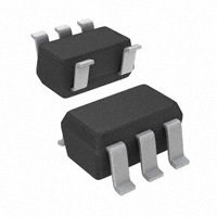
DBV PACKAGE
(TOP VIEW)
OUT 1
5 V+
GND 2
VIN+ 3
4 VIN-
DESCRIPTION
The INA193A current shunt monitors with voltage output can sense drops across shunts at common-mode
voltages from –16 V to 80 V, independent of the INA19x supply voltage. They are available with three output
voltage scales: 20 V/V, 50 V/V, and 100 V/V. The 500-kHz bandwidth simplifies use in current control loops.
The INA193A operates from a single 2.7-V to 18-V supply, drawing a maximum of 1300-μA of supply current. It
is specified over the extended operating temperature range (–55°C to 125°C), and is offered in a space-saving
SOT23 package.
1
Please be aware that an important notice concerning availability, standard warranty, and use in critical applications of
Texas Instruments semiconductor products and disclaimers thereto appears at the end of this data sheet.
PRODUCTION DATA information is current as of publication date.
Products conform to specifications per the terms of the Texas
Instruments standard warranty. Production processing does not
necessarily include testing of all parameters.
Copyright © 2007–2013, Texas Instruments Incorporated
�INA193A-EP
SBOS400A – MAY 2007 – REVISED SEPTEMBER 2013
www.ti.com
This integrated circuit can be damaged by ESD. Texas Instruments recommends that all integrated circuits be handled with
appropriate precautions. Failure to observe proper handling and installation procedures can cause damage.
ESD damage can range from subtle performance degradation to complete device failure. Precision integrated circuits may be more
susceptible to damage because very small parametric changes could cause the device not to meet its published specifications.
ORDERING INFORMATION (1)
TA
–55°C to 125°C
(1)
(2)
PACKAGE
(2)
ORDERABLE PART NUMBER
TOP-SIDE MARKING
INA193AMDBVREP
CCC
SOT23-5 – DBV
For the most current package and ordering information, see the Package Option Addendum at the end of this document, or see the TI
website at www.ti.com.
Package drawings, standard packing quantities, thermal data, symbolization, and PCB design guidelines are available at
www.ti.com/sc/package.
MODEL
GAIN
PACKAGE
INA193A
20 V/V
SOT23-5
IS
RS
VIN+
-16 V to 80 V
Negative
and
Positive
Common-Mode
Voltage
V+
2.7 V to 18 V
VIN+
VIN-
R1
R1
Load
A1
-
+
+
A2
OUT
INA193A
2
RL
Submit Documentation Feedback
Copyright © 2007–2013, Texas Instruments Incorporated
Product Folder Links: INA193A-EP
�INA193A-EP
www.ti.com
SBOS400A – MAY 2007 – REVISED SEPTEMBER 2013
Absolute Maximum Ratings (1)
over operating free-air temperature range (unless otherwise noted)
MIN
MAX
Supply voltage
VIN+
VIN–
18
–18
18
Common mode (2)
–16
80
GND – 0.3
(V+) + 0.3
5
mA
Operating temperature range
–55
150
°C
Storage temperature range
–65
150
°C
150
°C
Analog input voltage range
Input current into any pin
OUT
(2)
Junction temperature
ESD ratings
(2)
V
Differential (VIN+ – VIN–)
Analog outputt voltage range (2)
(1)
UNIT
Human-Body Model (HBM)
4000
Charged-Device Model (CDM)
1000
V
V
V
Stresses beyond those listed under "absolute maximum ratings" may cause permanent damage to the device. These are stress ratings
only, and functional operation of the device at these or any other conditions beyond those indicated under "recommended operating
conditions" is not implied. Exposure to absolute-maximum-rated conditions for extended periods may affect device reliability.
Input voltage at any pin may exceed the voltage shown if the current at that pin is limited to 5 mA.
Electrical Characteristics
VS = + 12 V. Boldface limits apply over the specified temperature range, TA = –55°C to 125°C. All specifications at
TA = 25°C, VS = 12 V, VIN+ = 12 V, and VSENSE = 100 mV (unless otherwise noted).
PARAMETER
TEST CONDITIONS
MIN
TYP
MAX
UNIT
0.15
(VS – 0.2)/Gain
V
80
V
INPUT
Full-scale input voltage
Common-mode input range
Common-mode rejection
VSENSE VSENSE = VIN+ – VIN–
VCM
CMR VIN+ = –16 V to 80 V
Over temperature
Offset voltage, RTI
–16
VIN+ = 12 V to 80 V
VOS
Over temperature
vs temperature
vs power supply
Input bias current, VIN– pin
dVOS/dT
80
94
100
120
dB
dB
±0.5
2
0.5
3
IB
mV
μV/°C
2.5
PSR VS = 2.7 V to 18 V, VIN+ = 18 V
mV
5
100
μV/V
±8
±23
μA
OUTPUT (VSENSE ≥ 20 mV)
Gain
G
20
VSENSE = 20 mV to 100 mV,
TA = 25°C
Gain error
Over temperature
Over temperature
Nonlinearity error
Output impedance
Maximum capacitive load
(1)
±0.2
±1
%
±2
%
±0.75
±2.2
%
±1
±3
%
±0.002
±0.1
%
VSENSE = 20 mV to 100 mV
Total output error (1)
VSENSE = 20 mV to 100 mV
RO
No sustained oscillation
V/V
1.5
Ω
10
nF
Total output error includes effects of gain error and VOS.
Submit Documentation Feedback
Copyright © 2007–2013, Texas Instruments Incorporated
Product Folder Links: INA193A-EP
3
�INA193A-EP
SBOS400A – MAY 2007 – REVISED SEPTEMBER 2013
www.ti.com
Electrical Characteristics (continued)
VS = + 12 V. Boldface limits apply over the specified temperature range, TA = –55°C to 125°C. All specifications at
TA = 25°C, VS = 12 V, VIN+ = 12 V, and VSENSE = 100 mV (unless otherwise noted).
PARAMETER
TEST CONDITIONS
MIN
TYP
MAX
UNIT
OUTPUT (VSENSE < 20 mV) (2)
–16 V ≤ VCM < 0 V
300
0 V ≤ VCM ≤ VS, VS = 5 V
VS < VCM ≤ 80 V
VOLTAGE OUTPUT (3)
mV
0.4
300
V
mV
RL = 100 KΩ to GND
Swing to V+ power-supply rail
Swing to GND (4)
(V+) – 0.1
(V+) – 0.2
V
VGND + 3
VGND + 50
mV
FREQUENCY RESPONSE
Bandwidth
BW CLOAD = 5 pF
Phase margin
Slew rate
Settling time (1%)
CLOAD < 10 nF
SR
tS
VSENSE = 10 mV to 100 mVPP,
CLOAD = 5 pF
500
kHz
40
Degrees
1
V/μs
2
μs
40
nV/√Hz
NOISE, RTI
Voltage noise density
POWER SUPPLY
Operating range
Quiescent Current
VS
2.7
IQ VOUT = 2 V
VSENSE = 0 mV
18
V
700
1300
μA
370
950
μA
TEMPERATURE RANGE
Specified temperature range
–55
125
°C
Operating temperature range
–55
150
°C
Storage temperature range
–65
150
Thermal resistance, SOT23
(2)
(3)
(4)
4
θJA
200
°C
°C/W
For details on this region of operation, see the Accuracy Variations as a Result of VSENSE and Common-Mode Voltage section in the
Applications Information.
See Typical Characteristic curve Output Swing vs Output Current.
Specified by design
Submit Documentation Feedback
Copyright © 2007–2013, Texas Instruments Incorporated
Product Folder Links: INA193A-EP
�INA193A-EP
www.ti.com
SBOS400A – MAY 2007 – REVISED SEPTEMBER 2013
TYPICAL CHARACTERISTICS
All specifications at TA = 25°C, VS = 12 V, and VIN+ = 12 V, and VSENSE = 100 mV (unless otherwise noted).
GAIN
vs
FREQUENCY
GAIN
vs
FREQUENCY
45
45
40
G = 50
35
Gain (dB)
30
G = 100
40
G = 50
35
Gain (dB)
CLOAD = 1000pF
G = 100
G = 20
25
20
30
20
15
15
10
10
5
G = 20
25
5
10k
100k
10k
1M
100k
Frequency (Hz)
COMMON-MODE AND POWER-SUPPLY REJECTION
vs
FREQUENCY
GAIN PLOT
20
140
18
130
Common−Mode and
Power−Supply Rejection (dB)
100V/V
16
VOUT (V)
14
50V/V
12
10
8
20V/V
6
4
2
0
120
CMR
110
100
90
PSR
80
70
60
50
40
20
100
200
300
400
500
600
700
800
900
10
100
1k
VDIFFERENTIAL (mV)
10k
100k
Frequency (Hz)
OUTPUT ERROR
vs
VSENSE
4.0
OUTPUT ERROR
vs
COMMON-MODE VOLTAGE
0.1
0.09
3.5
0.08
3.0
Output Error (% )
Output Error
(% error of the ideal output value)
1M
Frequency (Hz)
2.5
2.0
1.5
1.0
0.07
0.06
0.05
0.04
0.03
0.02
0.5
0.01
0
0
50
100 150
200
250 300
350 400
450 500
0
−16 −12 −8 −4
VSENSE (mV)
0
4
8
12 16 20
...
76 80
Common−Mode Voltage (V)
Submit Documentation Feedback
Copyright © 2007–2013, Texas Instruments Incorporated
Product Folder Links: INA193A-EP
5
�INA193A-EP
SBOS400A – MAY 2007 – REVISED SEPTEMBER 2013
www.ti.com
TYPICAL CHARACTERISTICS (continued)
All specifications at TA = 25°C, VS = 12 V, and VIN+ = 12 V, and VSENSE = 100 mV (unless otherwise noted).
POSITIVE OUTPUT VOLTAGE SWING
vs
OUTPUT CURRENT
QUIESCENT CURRENT
vs
OUTPUT VOLTAGE
1000
12
900
VS = 12V
10
9
800
Sourcing Current
+25_ C
8
700
−40_ C
+125_ C
7
6
IQ (µA)
Output Voltage (V )
11
VS = 3V
5
Sourcing Current
+25_ C
4
−40_ C
2
1
+125_ C
0
0
500
400
300
Output stage is designed
to source current. Current
sinking capability is
approximately 400µA.
3
600
200
100
0
5
10
25
20
15
30
0
1
2
Output Current (mA)
VS = 2.7V
IQ (µA)
675
575
475
VS = 12V
VS = 2.7V
275
Output Short−Circuit Current (mA)
VS = 12V
VSENSE = 0mV:
8
9
10
−40_C
30
+25_ C
26
+125_ C
22
18
14
10
6
0
4
8
12 16
20
...
2.5 3.5
76 80
VCM (V)
4.5
5.5 6.5
7.5
8.5
9.5 10.5 11.5 17
18
Supply Voltage (V)
STEP RESPONSE
STEP RESPONSE
G = 20
Output Voltage (50mV/div)
Output Voltage (500mV/div)
G = 20
VSENSE = 10mV to 20mV
VSENSE = 10mV to 100mV
Time (2µs/div)
Time (2µs/div)
6
7
6
34
VSENSE = 100mV:
175
−16 −12 −8 −4
5
OUTPUT SHORT-CIRCUIT CURRENT
vs
SUPPLY VOLTAGE
775
375
4
Output Voltage (V)
QUIESCENT CURRENT
vs
COMMON-MODE VOLTAGE
875
3
Submit Documentation Feedback
Copyright © 2007–2013, Texas Instruments Incorporated
Product Folder Links: INA193A-EP
�INA193A-EP
www.ti.com
SBOS400A – MAY 2007 – REVISED SEPTEMBER 2013
TYPICAL CHARACTERISTICS (continued)
All specifications at TA = 25°C, VS = 12 V, and VIN+ = 12 V, and VSENSE = 100 mV (unless otherwise noted).
STEP RESPONSE
STEP RESPONSE
G = 50
Output Voltage (50mV/div)
Output Voltage (100mV/div)
G = 20
VSENSE = 90mV to 100mV
VSENSE = 10mV to 20mV
Time (2µs/div)
Time (5µs/div)
STEP RESPONSE
STEP RESPONSE
G = 50
Output Voltage (1V/div)
Output Voltage (100mV/div)
G = 50
VSENSE = 10mV to 100mV
VSENSE = 90mV to 100mV
Time (5µs/div)
Time (5µs/div)
STEP RESPONSE
Output Voltage (2V/div)
G = 100
VSENSE = 10mV to 100mV
Time (10µs/div)
Submit Documentation Feedback
Copyright © 2007–2013, Texas Instruments Incorporated
Product Folder Links: INA193A-EP
7
�INA193A-EP
SBOS400A – MAY 2007 – REVISED SEPTEMBER 2013
www.ti.com
APPLICATION INFORMATION
Basic Connection
Figure 1 shows the basic connection of INA193A. The input pins, VIN+ and VIN–, should be connected as closely
as possible to the shunt resistor to minimize any resistance in series with the shunt resistance.
Power-supply bypass capacitors are required for stability. Applications with noisy or high impedance power
supplies may require additional decoupling capacitors to reject power supply noise. Connect bypass capacitors
close to the device pins.
RS
IS
VIN+
V+
2.7 V to 18 V
-16 V to 80 V
VIN+
VIN-
R1
R2
Load
OUT
INA193A
RL
Figure 1. INA193A Basic Connection
Power Supply
The input circuitry of the INA193A can accurately measure beyond its power supply voltage, V+. For example,
the V+ power supply can be 5 V, whereas the load power supply voltage is up to 80 V. The output voltage range
of the OUT terminal, however, is limited by the voltages on the power-supply pin.
Accuracy Variations as a Result of VSENSE and Common-Mode Voltage
The accuracy of the INA193A current shunt monitors is a function of two main variables:
VSENSE (VIN+ – VIN–) and common-mode voltage, VCM, relative to the supply voltage, VS. VCM is expressed as
(VIN+ + VIN–)/2; however, in practice, VCM is seen as the voltage at VIN+ because the voltage drop across VSENSE
is usually small.
8
Submit Documentation Feedback
Copyright © 2007–2013, Texas Instruments Incorporated
Product Folder Links: INA193A-EP
�INA193A-EP
www.ti.com
SBOS400A – MAY 2007 – REVISED SEPTEMBER 2013
This section addresses the accuracy of these specific operating regions:
Normal Case 1:
VSENSE ≥ 20 mV, VCM ≥ VS
Normal Case 2:
VSENSE ≥ 20 mV, VCM < VS
Low VSENSE Case 1:
VSENSE < 20 mV, –16 V ≤ VCM < 0
Low VSENSE Case 2:
VSENSE < 20 mV, 0 V ≤ VCM ≤ VS
Low VSENSE Case 3:
VSENSE < 20 mV, VS < VCM ≤ 80 V
Normal Case 1: VSENSE ≥ 20 mV, VCM ≥ VS
This region of operation provides the highest accuracy. Here, the input offset voltage is characterized and
measured using a two-step method. First, the gain is determined by (Equation 1).
V OUT1 * V OUT2
G+
100 mV * 20 mV
(1)
Where:
VOUT1 = Output voltage with VSENSE = 100 mV
VOUT2 = Output voltage with VSENSE = 20 mV
The offset voltage is then measured at VSENSE = 100 mV and referred to the input (RTI) of the current shunt
monitor, as shown in (Equation 2).
V OSRTI (Referred−To−Input) +
ǒV G Ǔ * 100 mV
OUT1
(2)
In the Typical Characteristics, the Output Error vs Common-Mode Voltage curve shows the highest accuracy for
the this region of operation. In this plot, VS = 12 V; for VCM ≥ 12 V, the output error is at its minimum. This case is
also used to create the VSENSE ≥ 20 mV output specifications in the Electrical Characteristics table.
Normal Case 2: VSENSE ≥ 20 mV, VCM < VS
This region of operation has slightly less accuracy than Normal Case 1 as a result of the common-mode
operating area in which the part functions, as seen in the Output Error vs Common-Mode Voltage curve. As
noted, for this graph VS = 12 V; for VCM < 12 V, the Output Error increases as VCM becomes less than 12 V, with
a typical maximum error of 0.005% at the most negative VCM = –16 V.
Low VSENSE Case 1: VSENSE < 20 mV, –16 V ≤ VCM < 0; and Low VSENSE Case 3: VSENSE < 20 mV,
VS < VCM ≤ 80 V
Although the INA193A is not designed for accurate operation in either of these regions, some applications are
exposed to these conditions; for example, when monitoring power supplies that are switched on and off while VS
is still applied to the INA193A. It is important to know what the behavior of the devices will be in these regions.
As VSENSE approaches 0 mV, in these VCM regions, the device output accuracy degrades. A larger-than-normal
offset can appear at the current shunt monitor output with a typical maximum value of VOUT = 300 mV for
VSENSE = 0 mV. As VSENSE approaches 20 mV, VOUT returns to the expected output value with accuracy as
specified in the Electrical Characteristics. Figure 2 illustrates this effect using the INA195A and INA198A
(Gain = 100).
Submit Documentation Feedback
Copyright © 2007–2013, Texas Instruments Incorporated
Product Folder Links: INA193A-EP
9
�INA193A-EP
SBOS400A – MAY 2007 – REVISED SEPTEMBER 2013
www.ti.com
2.0
1.8
1.6
VOUT (V)
1.4
1.2
Actual
1.0
0.8
Ideal
0.6
0.4
0.2
0
0
2
4
6
8
10
12
14
16
18
20
VSENSE (mV)
Figure 2. Example for Low VSENSE Cases 1 and 3
(INA195A, INA198A: Gain = 100)
Low VSENSE Case 2: VSENSE < 20 mV, 0 V ≤ VCM ≤ VS
This region of operation is the least accurate for the INA193A. To achieve the wide input common-mode voltage
range, these devices use two op amp front ends in parallel. One op amp front end operates in the positive input
common-mode voltage range, and the other in the negative input region. For this case, neither of these two
internal amplifiers dominates and overall loop gain is very low. Within this region, VOUT approaches voltages
close to linear operation levels for Normal Case 2. This deviation from linear operation becomes greatest the
closer VSENSE approaches 0 V. Within this region, as VSENSE approaches 20 mV, device operation is closer to that
described by Normal Case 2. Figure 3 illustrates this behavior for the INA195A. The VOUT maximum peak for this
case is tested by maintaining a constant VS, setting VSENSE = 0 mV and sweeping VCM from 0 V to VS. The exact
VCM at which VOUT peaks during this test varies from part to part, but the VOUT maximum peak is tested to be less
than the specified VOUT tested limit.
2.4
INA195, INA198 VOUT Tested Limit(1)
VCM1
2.2
2.0
Ideal
1.8
VCM2
VOUT (V)
1.6
1.4
VCM3
1.2
1.0
VOUT tested limit at
VSENSE = 0mV, 0 ≤ VCM1 ≤ VS.
VCM4
0.8
0.6
VCM2, VCM3, and VCM4 illustrate the variance
from part to part of the VCM that can cause
maximum VOUT with VSENSE < 20mV.
0.4
0.2
0
0
2
4
6
8
10
12
14
16
18
20
22
24
VSENSE (mV)
NOTE: (1) INA193, INA196 VOUT Tested Limit = 0.4V.
INA194, INA197 VOUT Tested Limit = 1V.
Figure 3. Example for Low VSENSE Case 2
(INA195A, INA198A: Gain = 100)
10
Submit Documentation Feedback
Copyright © 2007–2013, Texas Instruments Incorporated
Product Folder Links: INA193A-EP
�INA193A-EP
www.ti.com
SBOS400A – MAY 2007 – REVISED SEPTEMBER 2013
Shutdown
Because the INA193A consumes a quiescent current less than 1 mA, it can be powered by either the output of
logic gates or by transistor switches to supply power. Use a totem pole output buffer or gate that can provide
sufficient drive along with 0.1-μF bypass capacitor, preferably ceramic with good high frequency characteristics.
This gate should have a supply voltage of 3 V or greater because the INA193A requires a minimum supply
greater than 2.7 V. In addition to eliminating quiescent current, this gate also turns off the 10 μA bias current
present at each of the inputs. An example shutdown circuit is shown in Figure 4.
IL
RS
VIN+
-16 V to 80 V
Negative
and
Positive
Common-Mode
Voltage
VIN+
VIN-
R1
R2
V+
Load
V+ > 3 V
A1
0.1 mF
A2
OUT
INA193A
RL
Figure 4. INA193A Example Shutdown Circuit
Selecting RS
The value chosen for the shunt resistor, RS, depends on the application and is a compromise between smallsignal accuracy and maximum permissible voltage loss in the measurement line. High values of RS provide better
accuracy at lower currents by minimizing the effects of offset, while low values of RS minimize voltage loss in the
supply line. For most applications, best performance is attained with an RS value that provides a full-scale shunt
voltage range of 50 mV to 100 mV. Maximum input voltage for accurate measurements is 500 mV.
Transient Protection
The –16 V to 80 V common-mode range of the INA193A is ideal for withstanding automotive fault conditions
ranging from 12-V battery reversal up to 80-V transients, since no additional protective components are needed
up to those levels. In the event that the INA193A is exposed to transients on the inputs in excess of its ratings,
then external transient absorption with semiconductor transient absorbers (zeners or Transzorbs) will be
necessary. Use of MOVs or VDRs is not recommended except when they are used in addition to a
semiconductor transient absorber. Select the transient absorber such that it will never allow the INA193A to be
exposed to transients greater than 80 V (that is, allow for transient absorber tolerance, as well as additional
voltage due to transient absorber dynamic impedance). Despite the use of internal zener type ESD protection,
the INA193A– does not lend itself to using external resistors in series with the inputs since the internal gain
resistors can vary up to ±30% (if gain accuracy is not important, then resistors can be added in series with the
INA193A inputs with two equal resistors on each input).
Submit Documentation Feedback
Copyright © 2007–2013, Texas Instruments Incorporated
Product Folder Links: INA193A-EP
11
�INA193A-EP
SBOS400A – MAY 2007 – REVISED SEPTEMBER 2013
www.ti.com
Output Voltage Range
The output of the INA193A is accurate within the output voltage swing range set by the power-supply pin, V+.
This is best illustrated when using the INA195A or INA198A (which are both versions using a gain of 100), where
a 100 mV full-scale input from the shunt resistor requires an output voltage swing of 10 V, and a power-supply
voltage sufficient to achieve 10 V on the output.
RFI/EMI
Attention to good layout practices is always recommended. Keep traces short and, when possible, use a printed
circuit board (PCB) ground plane with surface-mount components placed as close to the device pins as possible.
Small ceramic capacitors placed directly across amplifier inputs can reduce RFI/EMI sensitivity. PCB layout
should locate the amplifier as far away as possible from RFI sources. Sources can include other components in
the same system as the amplifier itself, such as inductors (particularly switched inductors handling a lot of current
and at high frequencies). RFI can generally be identified as a variation in offset voltage or dc signal levels with
changes in the interfering RF signal. If the amplifier cannot be located away from sources of radiation, shielding
may be needed. Twisting wire input leads makes them more resistant to RF fields.
Input Filtering
An obvious and straightforward location for filtering is at the output of the INA193A; however, this location
negates the advantage of the low output impedance of the internal buffer. The only other option for filtering is at
the input pins of the INA193A, which is complicated by the internal 5-kΩ + 30% input impedance; this is
illustrated in Figure 5. Using the lowest possible resistor values minimizes both the initial shift in gain and effects
of tolerance. The effect on initial gain is given by:
ǒ
GainError% + 100 * 100
Ǔ
5k W
5k W ) RFILT
(3)
Total effect on gain error can be calculated by replacing the 5-kΩ term with 5 kΩ – 30%, (or 3.5 kΩ) or
5 kΩ + 30% (or 6.5 kΩ). The tolerance extremes of RFILT can also be inserted into the equation. If a pair of 100-Ω
1% resistors are used on the inputs, the initial gain error will be approximately 2%. Worst-case tolerance
conditions will always occur at the lower excursion of the internal 5-kΩ resistor (3.5 kΩ), and the higher excursion
of RFILT – 3% in this case. Note that the specified accuracy of the INA193A must then be combined in addition to
these tolerances. While this discussion treated accuracy worst-case conditions by combining the extremes of the
resistor values, it is appropriate to use geometric mean or root sum square calculations to total the effects of
accuracy variations.
12
Submit Documentation Feedback
Copyright © 2007–2013, Texas Instruments Incorporated
Product Folder Links: INA193A-EP
�INA193A-EP
www.ti.com
SBOS400A – MAY 2007 – REVISED SEPTEMBER 2013
RSHUNT comparator trip-point.
R1
OUT
TLV3012
INA193A
R2
REF
1.25-V
Internal
Reference
(a) INA193A output adjusted by voltage divider
VIN+
VIN-
V+
OUT
TLV3012
INA193A
R1
(b) Comparator reference voltage adjusted by voltage divider
R2
REF
1.25-V
Internal
Reference
For use with
small output signals
Figure 10. INA193A With Comparator
Submit Documentation Feedback
Copyright © 2007–2013, Texas Instruments Incorporated
Product Folder Links: INA193A-EP
17
�PACKAGE OPTION ADDENDUM
www.ti.com
10-Dec-2020
PACKAGING INFORMATION
Orderable Device
Status
(1)
Package Type Package Pins Package
Drawing
Qty
Eco Plan
(2)
Lead finish/
Ball material
MSL Peak Temp
Op Temp (°C)
Device Marking
(3)
(4/5)
(6)
INA193AMDBVREP
ACTIVE
SOT-23
DBV
5
3000
RoHS & Green
NIPDAU
Level-2-260C-1 YEAR
-55 to 125
CCC
V62/07638-01XE
ACTIVE
SOT-23
DBV
5
3000
RoHS & Green
NIPDAU
Level-2-260C-1 YEAR
-55 to 125
CCC
(1)
The marketing status values are defined as follows:
ACTIVE: Product device recommended for new designs.
LIFEBUY: TI has announced that the device will be discontinued, and a lifetime-buy period is in effect.
NRND: Not recommended for new designs. Device is in production to support existing customers, but TI does not recommend using this part in a new design.
PREVIEW: Device has been announced but is not in production. Samples may or may not be available.
OBSOLETE: TI has discontinued the production of the device.
(2)
RoHS: TI defines "RoHS" to mean semiconductor products that are compliant with the current EU RoHS requirements for all 10 RoHS substances, including the requirement that RoHS substance
do not exceed 0.1% by weight in homogeneous materials. Where designed to be soldered at high temperatures, "RoHS" products are suitable for use in specified lead-free processes. TI may
reference these types of products as "Pb-Free".
RoHS Exempt: TI defines "RoHS Exempt" to mean products that contain lead but are compliant with EU RoHS pursuant to a specific EU RoHS exemption.
Green: TI defines "Green" to mean the content of Chlorine (Cl) and Bromine (Br) based flame retardants meet JS709B low halogen requirements of