INA209
INA
209
www.ti.com ......................................................................................................................................................... SBOS403B – JUNE 2007 – REVISED MARCH 2009
High-Side Measurement, Bi-Directional Current/Power Monitor
with I2C™ Interface
FEATURES
DESCRIPTION
1
• SENSES BUS VOLTAGES FROM 0V TO +26V
• REPORTS CURRENT, VOLTAGE, AND
POWER; STORES PEAKS
• TRIPLE WATCHDOG LIMITS:
– Lower Warning with Delay
– Upper Over-limit, No Delay
– Fast Analog Critical
• HIGH ACCURACY: 1% MAX OVER TEMP
23
APPLICATIONS
•
•
•
•
•
•
•
•
SERVERS
TELECOM EQUIPMENT
AUTOMOTIVE
POWER MANAGEMENT
BATTERY CHARGERS
WELDING EQUIPMENT
POWER SUPPLIES
TEST EQUIPMENT
VIN+ VIN-
The INA209 also includes an analog comparator and
a programmable digital-to-analog converter (DAC)
that combine to provide the fastest possible
responses to current overload conditions.
The INA209 can be used together with hot swap
controllers that already use a current sense resistor.
The INA209 full-scale range can be selected to be
either within the hot-swap controller sense limits, or
wide enough to include them.
VS
(Supply Voltage)
INA209
Critical
DAC +
CMP
Filter
Critical
DAC -
The INA209 is a high-side current shunt and power
monitor with an I2C interface. The INA209 monitors
both shunt drop and shunt bus voltage. A
programmable calibration value, combined with an
internal multiplier, enables direct readouts in
amperes. An additional multiplying register calculates
power in watts. The INA209 features two separate,
onboard watchdog capabilities: a warning comparator
and an over-limit comparator. The warning
comparator is useful for monitoring lower warning
limits and incorporates a user-defined delay. The
over-limit comparator assists with monitoring upper
limits that could require immediate system shutdown.
Critical
The INA209 senses across shunts on buses that can
vary from 0V to 26V. The device uses a single +3V to
+5.5V supply, drawing a maximum of 1.5mA of
supply current. It is specified for operation from
–25°C to +85°C.
CMP
Overlimit
Watchdog
Warning
´
Power Register
Alert
2
IC
Interface
Current Register
ADC
Data
CLK
Voltage Register
GND
Convert
GPIO
1
2
3
Please be aware that an important notice concerning availability, standard warranty, and use in critical applications of Texas
Instruments semiconductor products and disclaimers thereto appears at the end of this data sheet.
I2C is a trademark of NXP Semiconductors.
All other trademarks are the property of their respective owners.
PRODUCTION DATA information is current as of publication date.
Products conform to specifications per the terms of the Texas
Instruments standard warranty. Production processing does not
necessarily include testing of all parameters.
Copyright © 2007–2009, Texas Instruments Incorporated
�INA209
SBOS403B – JUNE 2007 – REVISED MARCH 2009 ......................................................................................................................................................... www.ti.com
This integrated circuit can be damaged by ESD. Texas Instruments recommends that all integrated circuits be handled with
appropriate precautions. Failure to observe proper handling and installation procedures can cause damage.
ESD damage can range from subtle performance degradation to complete device failure. Precision integrated circuits may be more
susceptible to damage because very small parametric changes could cause the device not to meet its published specifications.
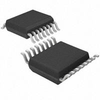
ORDERING INFORMATION (1)
(1)
PRODUCT
PACKAGE-LEAD
PACKAGE DESIGNATOR
PACKAGE MARKING
INA209
TSSOP-16
PW
INA209A
For the most current package and ordering information see the Package Option Addendum at the end of this document, or see the TI
web site at www.ti.com.
ABSOLUTE MAXIMUM RATINGS (1)
Over operating free-air temperature range (unless otherwise noted).
Supply Voltage, VS
Analog Inputs,
VIN+, VIN–
INA209
UNIT
6
V
Differential (VIN+) – (VIN–) (2)
–26 to +26
V
Common-Mode
–0.3 to +26
V
GND – 0.3 to +6
V
Open-Drain Digital Outputs
GPIO, Convert Pins
Input Current Into Any Pin
Open-Drain Digital Output Current
GND – 0.3 to VS + 0.3
V
5
mA
10
mA
Operating Temperature
–40 to +125
°C
Storage Temperature
–65 to +150
°C
Junction Temperature
+150
°C
Human Body Model
2000
V
Charged-Device Model
1000
V
Machine Model (MM)
150
V
ESD Ratings
(1)
(2)
2
Stresses above these ratings may cause permanent damage. Exposure to absolute maximum conditions for extended periods may
degrade device reliability. These are stress ratings only, and functional operation of the device at these or any other conditions beyond
those specified is not implied.
VIN+ and VIN– may have a differential voltage of –26V to +26V; however, the voltage at these pins must not exceed the range –0.3V to
+26V.
Submit Documentation Feedback
Copyright © 2007–2009, Texas Instruments Incorporated
Product Folder Link(s): INA209
�INA209
www.ti.com ......................................................................................................................................................... SBOS403B – JUNE 2007 – REVISED MARCH 2009
ELECTRICAL CHARACTERISTICS: VS = +3.3V
Boldface limits apply over the specified temperature range, TA = –25°C to +85°C.
At TA = +25°C, VIN+ = 12V, VSENSE = (VIN+ – VIN–) = 32mV, PGA = ÷ 1, and BRNG (1) = 1, unless otherwise noted.
INA209
PARAMETER
TEST CONDITIONS
MIN
PGA = ÷ 1
0
PGA = ÷ 2
PGA = ÷ 4
TYP
MAX
UNIT
±40
mV
0
±80
mV
0
±160
mV
PGA = ÷ 8
0
±320
mV
BRNG = 1
0
32
V
BRNG = 0
0
16
VIN+ = 0V to 26V
100
INPUT
Full-Scale Current Sense (Input) Voltage Range
Bus Voltage (Input Voltage) Range (2)
Common-Mode Rejection
CMRR
Offset Voltage, RTI (3)
VOS
PSRR
±10
±100
µV
PGA = ÷ 2
±20
±125
µV
PGA = ÷ 4
±30
±150
µV
PGA = ÷ 8
±40
±200
VS = 3V to 5.5V
Current Sense Gain Error
vs Temperature
Input Impedance
V
dB
PGA = ÷ 1
vs Temperature
vs Power Supply
120
µV
0.1
µV/°C
10
µV/V
±40
m%
10
ppm/°C
Active Mode
VIN+ Pin
20
µA
VIN– Pin
20 || 320
µA || kΩ
Input Leakage
Power-Down Mode
VIN+ Pin
0.1
±0.5
µA
VIN– Pin
0.1
±0.5
µA
DC ACCURACY
ADC Basic Resolution
12
Bits
1 LSB Step Size
Shunt Voltage
10
µV
Bus Voltage
4
mV
Current Measurement Error
±0.2
over Temperature
Bus Voltage Measurement Error
±0.2
over Temperature
%
±1
%
±0.5
%
±1
Differential Nonlinearity
±0.1
Critical DAC Full-Scale Range
255
Critical DAC Accuracy
±0.5
Critical DAC Resolution
mV
±1
mV
±0.3
Critical DAC Comparator Hysteresis (4)
See
Critical DAC Comparator Delay
%
Bits
1
Critical DAC Comparator Offset
%
LSB
8
Critical DAC 1 LSB Step Size
(1)
(2)
(3)
(4)
±0.5
±1.6
mV
(4)
5
µs
BRNG is bit 13 of the Configuration Register.
This parameter only expresses the full-scale range of the ADC scaling. In no event should more than 26V be applied to this device.
Referred-to-input (RTI).
User-programmable. See the Critical Comparator and Register sections.
Submit Documentation Feedback
Copyright © 2007–2009, Texas Instruments Incorporated
Product Folder Link(s): INA209
3
�INA209
SBOS403B – JUNE 2007 – REVISED MARCH 2009 ......................................................................................................................................................... www.ti.com
ELECTRICAL CHARACTERISTICS: VS = +3.3V (continued)
Boldface limits apply over the specified temperature range, TA = –25°C to +85°C.
At TA = +25°C, VIN+ = 12V, VSENSE = (VIN+ – VIN–) = 32mV, PGA = ÷ 1, and BRNG = 1, unless otherwise noted.
INA209
PARAMETER
TEST CONDITIONS
MIN
TYP
MAX
UNIT
12-Bit
532
586
µs
11-Bit
276
304
µs
10-Bit
148
163
µs
9-Bit
84
93
µs
ADC TIMING
ADC Conversion Time
Minimum Convert Input Low Time
µs
4
SMBus
SMBus Timeout (5)
28
35
ms
1
µA
V
DIGITAL INPUTS
(Convert, GPIO and SDA as Input, SCL, A0, A1)
Input Capacitance
3
0 ≤ VIN ≤ VS
Leakage Input Current
0.1
pF
Input Logic Levels:
VIH
0.7 (VS)
6
VIL
–0.3
0.3 (VS)
Hysteresis
500
V
mV
DIGITAL OUTPUTS
GPIO Pin Output Low
ISINK = 3mA
GPIO Pin Output High
ISOURCE = 3mA
0.15
VS – 0.4
0.4
VS – 0.15
V
V
OPEN-DRAIN DIGITAL OUTPUTS
(Critical, Over-Limit, Warning, Alert, SDA)
Logic '0' Output Level
High-Level Output Leakage Current
ISINK = 3mA
0.15
0.4
V
VOUT = VS
0.1
1
µA
POWER SUPPLY
Operating Supply Range
+5.5
V
Quiescent Current
+3
1
1.5
mA
Quiescent Current, Power-Down Mode
6
15
µA
Power-On Reset Threshold
2
V
TEMPERATURE RANGE
Specified Temperature Range
–25
+85
°C
Operating Temperature Range
–40
+125
°C
Thermal Resistance
θJA
TSSOP-16
(5)
4
+150
°C/W
SMBus timeout in the INA209 resets the interface any time SCL or SDA is low for over 28ms.
Submit Documentation Feedback
Copyright © 2007–2009, Texas Instruments Incorporated
Product Folder Link(s): INA209
�INA209
www.ti.com ......................................................................................................................................................... SBOS403B – JUNE 2007 – REVISED MARCH 2009
PIN CONFIGURATION
INA209
Top View
VIN+
1
16 SMBus Alert
VIN-
2
15 A1
Convert
3
14 A0
GND
4
13 SDA
VS+
5
12 SCL
GPIO
6
11 GND
Critical
7
10 VS+
Overlimit
8
9
Warning
PIN DESCRIPTIONS
PIN NO.
NAME
DESCRIPTION
1
VIN+
Positive differential shunt voltage. Connect to positive side of shunt resistor.
2
VIN–
Negative differential shunt voltage. Connect to negative side of shunt resistor. Bus voltage is measured
from this pin to ground.
3
Convert
Used to trigger conversions in triggered mode. In triggered mode, this pin should normally be high and
taken low to initiate conversion. It may be returned high after 4µs. If held low, the ADC converts each
time a triggered mode command is written via the I2C bus. If not used, this line should be tied high.
4
GND
5
VS+
6
GPIO
General-purpose, user-programmable input/output. Totem-pole output. Connect to ground or supply if
not used. Default state is as an input.
7
Critical
Open-drain critical watchdog output (filter set in Critical DAC– Register). Default state is disabled;
active-low; transparent (non-latched).
8
Overlimit
Open-drain over-limit watchdog output. Default state is disabled; active-low; transparent (non-latched).
9
Warning
Open-drain warning watchdog output (delay set in Critical DAC– Register). Default state is disabled;
active-low; transparent (non-latched).
Connect together with pin 11 to ground.
Connect together with pin 10 to supply, 3V to 5.5V.
10
VS+
11
GND
Connect together with pin 5 to supply, 3V to 5.5V.
Connect together with pin 4 to ground.
12
SCL
Serial bus clock line.
13
SDA
Serial bus data line.
14
A0
Address pin. Table 1 shows pin settings and corresponding addresses.
15
A1
Address pin. Table 1 shows pin settings and corresponding addresses.
16
SMBus Alert
Open-drain SMBus alert output. Controlled in SMBus Alert Mask Register. Default state is disabled.
Submit Documentation Feedback
Copyright © 2007–2009, Texas Instruments Incorporated
Product Folder Link(s): INA209
5
�INA209
SBOS403B – JUNE 2007 – REVISED MARCH 2009 ......................................................................................................................................................... www.ti.com
TYPICAL CHARACTERISTICS
At TA = +25°C, VIN+ = 12V, VSENSE = (VIN+ – VIN–) = 32mV, PGA = ÷ 1, and BRNG = 1, unless otherwise noted.
ADC SHUNT OFFSET vs TEMPERATURE
100
-10
80
-20
60
-30
40
Offset (mV)
Gain (dB)
FREQUENCY RESPONSE
0
-40
-50
-60
20
0
-20
-70
-40
-80
-60
-90
-80
-100
-100
100
10
1k
10k
100k
320mV Range
160mV Range
1M
80mV Range
0
-40 -25
Input Frequency (Hz)
40mV Range
25
Figure 1.
80
45
60
40
40
35
160mV Range
0
-20
-40
125
30
25
20
16V Range
32V Range
15
80mV Range 40mV Range
-60
10
-80
5
0
-100
-40 -25
0
25
50
75
100
0
-40 -25
125
25
50
75
100
125
Temperature (°C)
Temperature (°C)
Figure 3.
Figure 4.
ADC BUS GAIN ERROR vs TEMPERATURE
INTEGRAL NONLINEARITY vs INPUT VOLTAGE
100
20
80
15
60
10
40
16V Range
20
INL (mV)
Gain Error (m%)
100
ADC BUS VOLTAGE OFFSET vs TEMPERATURE
50
Offset (mV)
Gain Error (m%)
ADC SHUNT GAIN ERROR vs TEMPERATURE
320mV Range
75
Figure 2.
100
20
50
Temperature (°C)
0
-20
0
-5
32V Range
-40
5
-10
-60
-15
-80
-100
-40 -25
0
25
50
75
100
125
-20
-0.4
Temperature (°C)
-0.2
-0.1
0
0.1
0.2
0.3
0.4
Input Voltage (V)
Figure 5.
6
-0.3
Figure 6.
Submit Documentation Feedback
Copyright © 2007–2009, Texas Instruments Incorporated
Product Folder Link(s): INA209
�INA209
www.ti.com ......................................................................................................................................................... SBOS403B – JUNE 2007 – REVISED MARCH 2009
TYPICAL CHARACTERISTICS (continued)
At TA = +25°C, VIN+ = 12V, VSENSE = (VIN+ – VIN–) = 32mV, PGA = ÷ 1, and BRNG = 1, unless otherwise noted.
CRITICAL COMPARATOR FULL-SCALE ERROR vs
TEMPERATURE
CRITICAL COMPARATOR OFFSET vs TEMPERATURE
1.0
0.8
0.8
0.6
0.6
Offset (mV)
0.4
Full-Scale Error (mV)
1.0
Critical Comparator +
0.2
0
-0.2
-0.4
Critical Comparator -
0.2
0
-0.2
-0.4
-0.6
-0.6
-0.8
-0.8
-1.0
Critical Comparator +
-1.0
0
-40 -25
Critical Comparator -
0.4
25
50
75
100
-40 -25
125
50
Figure 7.
Figure 8.
75
100
125
100
125
ACTIVE IQ vs TEMPERATURE
1.2
VS+ = 5V
VS = 5V
1.5
1.0
1.0
0.8
0.5
IQ (mA)
Input Currents (mA)
25
Temperature (°C)
INPUT CURRENTS WITH LARGE DIFFERENTIAL
VOLTAGES
(VIN+ at 12V, Sweep of VIN–)
2.0
0
Temperature (°C)
VS+ = 3V
0
VS+ = 3V
VS = 3V
0.6
0.4
-0.5
0.2
-1.0
VS+ = 5V
0
-1.5
0
10
5
15
20
25
30
-40 -25
25
50
Temperature (°C)
Figure 9.
Figure 10.
75
ACTIVE IQ vs I2C CLOCK FREQUENCY
SHUTDOWN IQ vs TEMPERATURE
16
1.4
14
1.2
12
1.0
IQ (mA)
10
IQ (mA)
0
VIN- Voltage (V)
VS = 5V
8
VS = 5V
0.8
VS = 3V
0.6
6
VS = 3V
4
0.4
0.2
2
0
0
-40 -25
0
25
50
75
100
125
1k
10k
100k
Temperature (°C)
SCL Frequency (Hz)
Figure 11.
Figure 12.
1M
Submit Documentation Feedback
Copyright © 2007–2009, Texas Instruments Incorporated
Product Folder Link(s): INA209
10M
7
�INA209
SBOS403B – JUNE 2007 – REVISED MARCH 2009 ......................................................................................................................................................... www.ti.com
TYPICAL CHARACTERISTICS (continued)
At TA = +25°C, VIN+ = 12V, VSENSE = (VIN+ – VIN–) = 32mV, PGA = ÷ 1, and BRNG = 1, unless otherwise noted.
SHUTDOWN IQ vs I2C CLOCK FREQUENCY
400
350
300
IQ (mA)
250
200
VS = 5V
150
100
VS = 3V
50
0
1k
10k
100k
1M
10M
SCL Frequency (Hz)
Figure 13.
8
Submit Documentation Feedback
Copyright © 2007–2009, Texas Instruments Incorporated
Product Folder Link(s): INA209
�Copyright © 2007–2009, Texas Instruments Incorporated
Product Folder Link(s): INA209
Bus Voltage
Channel
Shunt Voltage
Channel
ADC
(1)
(1)
(1)
(1)
(2)
Data Registers
PGA
(In Configuration Register)
Shunt Voltage
Full-Scale Calibration
Current
Bus Voltage
Power
CMP
CMP
´
´
DAC
DAC
(2)
(2)
Peak-Hold Registers
Shunt Voltage- Peak
(2)
(2)
Shunt Voltage+ Peak
Bus Voltage
(2)
Minimum Peak
Bus Voltage
(2)
Maximum Peak
Power Peak
Critical DAC-
(2)
Critical DAC Hysteresis
Critical DAC+
(2)
(2)
(2)
CMP
CMP
CMP
CMP
CMP
CMP
CMP
CMP
Latch and
Polarity
Warning Registers and Output
Programmable Delay
(set in
Critical DAC- Register)
Warning Output Default:
· Disabled
· Active Low
· Transparent (not latched)
Overlimit Registers and Output
Latch and
Polarity
Enable/Disable
in SMBus/Enable
Register
Enable/Disable
in SMBus/Enable
Register
Enable/Disable
in SMBus/Enable
Register
Overlimit Output Default:
· Disabled
· Active Low
· Transparent (not latched)
Latch and
Polarity
NOTES: Dashed line indicates the flag is in the Status Register.
(1) Read-only.
(2) Read/Write.
Shunt Voltage- Warning
Shunt Voltage+ Warning
Bus Voltage Under(2)
Voltage Warning
Bus Voltage Over(2)
Voltage Warning
Power Warning
(2)
(2)
Bus Under-Voltage Over-limit
Bus Over-Voltage Over-limit
Power Over-limit
(2)
Programmable Delay
(set in
Critical DAC- Register)
Critical Output Default:
· Disabled
· Active Low
· Transparent (not latched)
Warning
(Open-Drain)
Over-limit
(Open-Drain)
Critical
(Open-Drain)
INA209
www.ti.com ......................................................................................................................................................... SBOS403B – JUNE 2007 – REVISED MARCH 2009
FUNCTIONAL BLOCK DIAGRAM
Figure 14.
Submit Documentation Feedback
9
�INA209
SBOS403B – JUNE 2007 – REVISED MARCH 2009 ......................................................................................................................................................... www.ti.com
APPLICATION INFORMATION
The INA209 is a digital current-shunt monitor with an
I2C and SMBus-compatible interface. It provides
digital current, voltage, and power readings
necessary
for
accurate
decision-making
in
precisely-controlled systems. Programmable registers
allow flexible configuration for setting warning limits,
measurement
resolution,
and
continuousversus-triggered
operation.
Detailed
register
information appears at the end of this data sheet,
beginning with Table 2. See the Functional Block
Diagram for a block diagram of the INA209.
To address a specific device, the master initiates a
START condition by pulling the data signal line (SDA)
from a HIGH to a LOW logic level while SCL is HIGH.
All slaves on the bus shift in the slave address byte
on the rising edge of SCL, with the last bit indicating
whether a read or write operation is intended. During
the ninth clock pulse, the slave being addressed
responds to the master by generating an
Acknowledge and pulling SDA LOW.
Data transfer is then initiated and eight bits of data
are sent, followed by an Acknowledge bit. During
data transfer, SDA must remain stable while SCL is
HIGH. Any change in SDA while SCL is HIGH is
interpreted as a START or STOP condition.
The INA209 offers compatability with I2C and SMBus
interfaces. The I2C and SMBus protocols are
essentially compatible with each other. I2C will be
used throughout this document, with SMBus being
specified only when a difference between the two
systems is being addressed. Two bi-directional lines,
SCL and SDA, connect the INA209 to the bus. Both
SCL and SDA are open-drain connections. Figure 15
shows a typical application circuit.
Once all data have been transferred, the master
generates a STOP condition, indicated by pulling
SDA from LOW to HIGH while SCL is HIGH. The
INA209 includes a 28ms timeout on its interface to
prevent locking up an SMBus.
BUS OVERVIEW
The device that initiates the transfer is called a
master, and the devices controlled by the master are
slaves. The bus must be controlled by a master
device that generates the serial clock (SCL), controls
the bus access, and generates START and STOP
conditions.
Current
Shunt
Load
Supply Voltage
(INA209 Power Supply Range is
3V to 5.5V)
Supply
3.3V Supply
CBYPASS
0.1mF
VIN+ VIN-
INA209
VS
Critical
DAC +
CMP
Filter
Critical
DAC -
Critical Output
CMP
Overlimit Output
Watchdog
Warning Output
´
Power Register
Alert
2
Current Register
IC
Interface
Data (SDA)
ADC
Clock (SCL)
Voltage Register
GND
Convert
GPIO
Figure 15. Typical Application Circuit
10
Submit Documentation Feedback
Copyright © 2007–2009, Texas Instruments Incorporated
Product Folder Link(s): INA209
�INA209
www.ti.com ......................................................................................................................................................... SBOS403B – JUNE 2007 – REVISED MARCH 2009
Serial Bus Address
WRITING TO/READING FROM THE INA209
To communicate with the INA209, the master must
first address slave devices via a slave address byte.
The slave address byte consists of seven address
bits, and a direction bit indicating the intent of
executing a read or write operation.
Accessing a particular register on the INA209 is
accomplished by writing the appropriate value to the
register pointer. Refer to Table 2 for a complete list of
registers and corresponding addresses. The value for
the register pointer as shown in Figure 19 is the first
byte transferred after the slave address byte with the
R/W bit LOW. Every write operation to the INA209
requires a value for the register pointer.
The INA209 has two address pins, A0 and A1.
Table 1 describes the pin logic levels for each of the
16 possible addresses. The state of pins A0 and A1
is sampled on every bus communication and should
be set before any activity on the interface occurs. The
address pins are read at the start of each
communication event.
Table 1. INA209 Address Pins and
Slave Addresses
A1
A0
SLAVE ADDRESS
GND
GND
1000000
GND
VS+
1000001
GND
SDA
1000010
GND
SCL
1000011
VS+
GND
1000100
VS+
VS+
1000101
VS+
SDA
1000110
VS+
SCL
1000111
SDA
GND
1001000
SDA
VS+
1001001
SDA
SDA
1001010
SDA
SCL
1001011
SCL
GND
1001100
SCL
VS+
1001101
SCL
SDA
1001110
SCL
SCL
1001111
Serial Interface
The INA209 operates only as a slave device on the
I2C bus and SMBus. Connections to the bus are
made via the open-drain I/O lines SDA and SCL. The
SDA and SCL pins feature integrated spike
suppression filters and Schmitt triggers to minimize
the effects of input spikes and bus noise. The INA209
supports the transmission protocol for fast (1kHz to
400kHz) and high-speed (1kHz to 3.4MHz) modes.
All data bytes are transmitted most significant byte
first.
Writing to a register begins with the first byte
transmitted by the master. This byte is the slave
address, with the R/W bit LOW. The INA209 then
acknowledges receipt of a valid address. The next
byte transmitted by the master is the address of the
register to which data will be written. This register
address value updates the register pointer to the
desired register. The next two bytes are written to the
register addressed by the register pointer. The
INA209 acknowledges receipt of each data byte. The
master may terminate data transfer by generating a
START or STOP condition.
When reading from the INA209, the last value stored
in the register pointer by a write operation determines
which register is read during a read operation. To
change the register pointer for a read operation, a
new value must be written to the register pointer. This
write is accomplished by issuing a slave address byte
with the R/W bit LOW, followed by the register pointer
byte. No additional data are required. The master
then generates a START condition and sends the
slave address byte with the R/W bit HIGH to initiate
the read command. The next byte is transmitted by
the slave and is the most significant byte of the
register indicated by the register pointer. This byte is
followed by an Acknowledge from the master; then
the slave transmits the least significant byte. The
master acknowledges receipt of the data byte. The
master may terminate data transfer by generating a
Not-Acknowledge after receiving any data byte, or
generating a START or STOP condition. If repeated
reads from the same register are desired, it is not
necessary to continually send the register pointer
bytes; the INA209 retains the register pointer value
until it is changed by the next write operation.
Figure 16 and Figure 17 show read and write
operation timing diagrams, respectively. Note that
register bytes are sent most-significant byte first,
followed by the least significant byte. Figure 18
shows the timing diagram for the SMBus Alert
response operation. Figure 19 illustrates a typical
register pointer configuration.
Submit Documentation Feedback
Copyright © 2007–2009, Texas Instruments Incorporated
Product Folder Link(s): INA209
11
�INA209
SBOS403B – JUNE 2007 – REVISED MARCH 2009 ......................................................................................................................................................... www.ti.com
Start By
Master
1
1
1
1
0
0
A3
A2
A1
A0
(1)
R/W
Frame 1 Two-Wire Slave Address Byte
0
A3
A2
A1
A0
(1)
9
ACK By
INA209
R/W
1
P7
P6
9
ACK By
INA209
1
D15 D14
P4
P3
P2
D13
P1
Frame 2 Register Pointer Byte
P5
D12
D11 D10
D9
(2)
From
INA209
Frame 2 Data MSByte
9
ACK By
INA209
P0
1
D15 D14
D13
D8
9
1
D7
ACK By
Master
D9
Frame 3 Data MSByte
D12 D11 D10
NOTES: (1) The value of the Slave Address Byte is determined by the settings of the A0 and A1 pins.
Refer to Table 1.
(2) Read data is from the last register pointer location. If a new register is desired, the register
pointer must be updated. See Figure 19.
(3) ACK by Master can also be sent.
0
Frame 1 Two-Wire Slave Address Byte
D8
D6
9
ACK By
INA209
D5
1
D7
D4
D3
From
INA209
D5
D4
D2
D3
D1
(2)
D2
Frame 3 Data LSByte
D6
9
9
ACK By
INA209
D0
NoACK By
Master
D0
D1
Frame 4 Data LSByte
(3)
Stop
Stop By
Master
Product Folder Link(s): INA209
SCL
SDA
SCL
SDA
Start By
Master
NOTE (1): The value of the Slave Address Byte is determined by the settings of the A0 and A1 pins. Refer to Table 1.
Copyright © 2007–2009, Texas Instruments Incorporated
Submit Documentation Feedback
12
Figure 17. Timing Diagram for Read Word Format
Figure 16. Timing Diagram for Write Word Format
�INA209
www.ti.com ......................................................................................................................................................... SBOS403B – JUNE 2007 – REVISED MARCH 2009
ALERT
1
9
1
9
SCL
SDA
0
0
0
1
1
0
0
1
R/W
Start By
Master
0
0
A3
A2
ACK By
INA209
A1
A0
0
From
INA209
Frame 1 SMBus ALERT Response Address Byte
Frame 2 Slave Address Byte
NACK By
Master
Stop By
Master
(1)
NOTE (1): The value of the Slave Address Byte is determined by the settings of the A0 and A1 pins. Refer to Table 1.
Figure 18. Timing Diagram for SMBus ALERT
1
9
1
9
SCL
¼
SDA
1
0
0
A3
A2
A1
A0
R/W
Start By
Master
P7
P6
P5
P4
P3
P2
P1
ACK By
INA209
Frame 1 Two-Wire Slave Address Byte
(1)
P0
Stop
ACK By
INA209
Frame 2 Register Pointer Byte
NOTE (1): The value of the Slave Address Byte is determined by the settings of the A0 and A1 pins. Refer to Table 1.
Figure 19. Typical Register Pointer Set
Submit Documentation Feedback
Copyright © 2007–2009, Texas Instruments Incorporated
Product Folder Link(s): INA209
13
�INA209
SBOS403B – JUNE 2007 – REVISED MARCH 2009 ......................................................................................................................................................... www.ti.com
High-Speed I2C Mode
The master then generates a repeated start condition
(a repeated start condition has the same timing as
the start condition). After this repeated start condition,
the protocol is the same as F/S mode, except that
transmission speeds up to 3.4Mbps are allowed.
Instead of using a stop condition, repeated start
conditions should be used to secure the bus in
HS-mode. A stop condition ends the HS-mode and
switches all the internal filters of the INA209 to
support the F/S mode.
When the bus is idle, both the SDA and SCL lines are
pulled high by the pull-up devices. The master
generates a start condition followed by a valid serial
byte containing High-Speed (HS) master code
00001XXX. This transmission is made in fast
(400kbps) or standard (100kbps) (F/S) mode at no
more than 400kbps. The INA209 does not
acknowledge the HS master code, but does
recognize it and switches its internal filters to support
3.4Mbps operation.
t(LOW)
tF
tR
t(HDSTA)
SCL
t(HDSTA)
t(HIGH)
t(SUSTO)
t(SUSTA)
t(HDDAT)
t(SUDAT)
SDA
t(BUF)
P
S
S
P
Figure 20. Bus Timing Diagram
Bus Timing Diagram Definitions
FAST MODE
PARAMETER
HIGH-SPEED MODE
MIN
MAX
MIN
MAX
UNITS
SCL Operating Frequency
f(SCL)
0.001
0.4
0.001
3.4
MHz
Bus Free Time Between STOP and START
Condition
t(BUF)
600
160
ns
Hold time after repeated START condition.
After this period, the first clock is generated.
t(HDSTA)
100
100
ns
Repeated START Condition Setup Time
t(SUSTA)
100
100
ns
STOP Condition Setup Time
t(SUSTO)
100
100
ns
Data Hold Time
t(HDDAT)
0
0
ns
Data Setup Time
t(SUDAT)
100
10
ns
SCL Clock LOW Period
t(LOW)
1300
160
ns
SCL Clock HIGH Period
t(HIGH)
600
60
Clock/Data Fall Time
tF
Clock/Data Rise Time
Clock/Data Rise Time for SCLK ≤ 100kHz
14
ns
300
160
ns
tR
300
160
ns
tR
1000
Submit Documentation Feedback
ns
Copyright © 2007–2009, Texas Instruments Incorporated
Product Folder Link(s): INA209
�INA209
www.ti.com ......................................................................................................................................................... SBOS403B – JUNE 2007 – REVISED MARCH 2009
Power-Up Conditions
BASIC ADC FUNCTIONS
Power-up conditions apply to a software reset via the
RST bit (bit 15) in the Configuration Register, or the
I2C bus General Call Reset. At device power up, all
Status bits are masked. Warning, Over-Limit, Critical,
and SMBus Alert functions are disabled. All watchdog
outputs default to active low and transparent
(non-latched) modes.
The two analog inputs to the INA209, VIN+ and VIN–,
connect to a shunt resistor in the bus of interest. The
INA209 is typically powered by a separate supply
from +3V to +5.5V. The bus being sensed can vary
from 0V to 26V. There are no special considerations
for power-supply sequencing (for example, a bus
voltage can be present with the supply voltage off,
and vice-versa). The INA209 senses the small drop
across the shunt for shunt voltage, and senses the
voltage with respect to ground from VIN– for the bus
voltage. Figure 21 illustrates this operation.
VSHUNT = VIN+ - VINTypically < 50mV
Current
Shunt
Supply
Load
Supply
Voltage
VIN+ VIN-
INA209 Power Supply
3V to 5.5V
VS
INA209
Critical
DAC +
CMP
Filter
Critical
CMP
Critical
DAC -
Overlimit
VBUS = VIN- - GND
Watchdog
Range of 0V to 26V
Typical Application 12V
Warning
´
Power Register
Alert
2
IC
Interface
Current Register
ADC
Data
CLK
Voltage Register
GND
Convert
GPIO
Figure 21. INA209 Configured for Shunt and Bus Voltage Measurement
Submit Documentation Feedback
Copyright © 2007–2009, Texas Instruments Incorporated
Product Folder Link(s): INA209
15
�INA209
SBOS403B – JUNE 2007 – REVISED MARCH 2009 ......................................................................................................................................................... www.ti.com
When the INA209 is in the normal operating mode
(that is, MODE bits of the Configuration Register are
set to '111'), it continuously converts the shunt
voltage up to the number set in the shunt voltage
averaging function (Configuration Register, SADC
bits). The device then converts the bus voltage up to
the number set in the bus voltage averaging
(Configuration Register, BADC bits). The Mode
control in the Configuration Register also permits
selecting modes to convert only voltage or current,
either continuously or in response to an event
(triggered).
All current and power calculations are performed in
the background and do not contribute to conversion
time; conversion times shown in the Electrical
Characteristics table can be used to determine the
actual conversion time.
Power-Down mode reduces the quiescent current
and turns off current into the INA209 inputs, avoiding
any supply drain. Full recovery from Power-Down
requires 40µs. ADC Off mode (set by the
Configuration Register, MODE bits) stops all
conversions.
In triggered mode, the external Convert line becomes
active. Convert commands are initiated by taking the
Convert line low for a minimum of 4µs. The Convert
line may be connected high when unused. Any
re-trigger of the Convert line during a conversion is
ignored, and the Convert line state is disregarded
until the conversion ends. There are several available
triggered modes; however, all conversions are
performed repeatedly up to the number set in the
Averaging function (Configuration Register, BADC
and SADC bits).
If the Convert line is held low, writing any of the
triggered convert modes into the Configuration
Register (even if the desired mode is already
programmed into the register) triggers a single-shot
conversion.
Although the INA209 can be read at any time, and
the data from the last conversion remain available,
the Conversion Ready bit (Status Register, CNVR bit)
is provided to help co-ordinate one-shot or triggered
conversions. The Conversion Ready bit is set after all
conversions, averaging, and multiplication operations
are complete.
16
The Conversion Ready bit clears under these
conditions:
1. Writing to the Configuration Register, except
when configuring the MODE bits for Power Down
or ADC off (Disable) modes;
2. Reading the Status Register; or
3. Triggering a single-shot conversion with the
Convert pin.
Power Measurement
Current and bus voltage are converted at different
points in time, depending on the resolution and
averaging mode settings. For instance, when
configured for 12-bit and 128 sample averaging, up to
68ms in time between sampling these two values is
possible. Again, these calculations are performed in
the background and do not add to the overall
conversion time.
Peak-Hold Registers
Shunt voltage peak registers hold the lowest and
highest converted reading for the shunt value. The
shunt value may be either positive or negative; as a
result, there is a need for a sign bit in either register.
For instance, the Shunt Voltage Positive Peak
Register in most systems records a positive voltage;
in most unidirectional current measurement
applications, the Shunt Voltage Negative Peak
Register also records a positive voltage. However,
certain conditions can occur in normally unidirectional
systems that cause a negative polarity across the
shunt; these events are recorded in the Shunt
Voltage Negative Peak Register.
Peak-hold registers do not record conditions that
trigger a Critical Comparator shutdown. A Critical
Comparator shutdown occurs within 5µs of detecting
a critical condition, while the ADC conversion
necessary to record a peak-hold requires 532µs.
Therefore, a system shutdown removes the fault
before the analog-to-digital conversion (ADC) can
record it.
Submit Documentation Feedback
Copyright © 2007–2009, Texas Instruments Incorporated
Product Folder Link(s): INA209
�INA209
www.ti.com ......................................................................................................................................................... SBOS403B – JUNE 2007 – REVISED MARCH 2009
Critical Comparator
PGA Function
The Critical Comparator function is included to
provide the fastest possible response to overload
events. This function bypasses the digital circuit by
capturing the event in the analog domain.
If larger full-scale shunt voltages are desired, the
INA209 provides a PGA function that increases the
full-scale range up to 2, 4, or 8 times (320mV).
Additionally, the bus voltage measurement has two
full-scale ranges: 16V or 32V.
The Critical Comparator responds only to shunt
voltage, and can be programmed for a value from
0mV to 255mV (in 1mV increments) in the Critical
DAC+ and Critical DAC– Registers. Two thresholds
are provided, allowing users to set different
thresholds in systems where bi-directional current
measurement occurs. For example, a power supply
may readily allow sourcing of 10A, but must indicate
an alarm whenever sinking more than 1A. The
SMBus Alert Mask/Enable Control Register allows the
user to enable or disable the Critical pin output
through the CREN bit. The CREN bit affects only the
Critical pin; it does not affect the CRIT+ or CRIT–
flags within the Status Register.
The Critical Comparator output filter is set by the CF
bits of the Critical DAC– Register. This filter
determines the duration of time that the CMP output
must be continuously active (not toggling) to
propagate to the Critical pin output and set the CRIT+
or CRIT– flags within the Status Register.
While the Critical Comparator output filter provides
settings from 0ms to 0.96ms, the CMP is actually
strobed every 4µs, providing multiple samples per
delay period. For the Critical output pin to become
active, the critical condition must be true for every
sample during the specified delay period.
When using the Critical Comparator in unidirectional
applications, where the Critical DAC– Register is
unused, the Comparator could trip in error if the input
is near zero, because the comparator can have an
offset of up to ±1.5mV. Noise also contributes to false
tripping. To avoid false tripping in unidirectional
applications, the Critical DAC– should be
programmed to a value beyond –2mV to account for
the offset, and an additional amount to provide a
noise margin. Alternatively, the Critical DAC– can be
programmed to negative full-scale range (–255mV),
in order to eliminate false tripping.
Compatibility with TI Hot Swap Controllers
The INA209 is designed for compatibility with hot
swap controllers such the TI TPS2490. The TPS2490
uses a high-side shunt with a limit at 50mV; the
INA209 full-scale range of 40mV enables the use of
the same shunt for current sensing below this limit.
When sensing is required at (or through) the 50mV
sense point of the TPS2490, the PGA of the INA209
can be set to ÷2 to provide an 80mV full-scale range.
A typical application connects the Critical pin output
to the TPS2490 enable line; this configuration
enables user-programmable current limits. Note that
the latched mode should be used for the Critical pin
output to avoid oscillation at the trip level.
Filtering and Input Considerations
Measuring current is often noisy, and such noise can
be difficult to define. The INA209 offers several
options for filtering by choosing resolution and
averaging in the Configuration Register. These
filtering options can be set independently for either
voltage or current measurement.
The internal ADC is based on a delta-sigma (ΔΣ)
front-end with a 500kHz (±10%) typical sampling rate.
This architecture has good inherent noise rejection;
however, transients that occur at or very close to the
sampling rate harmonics can cause problems.
Because these signals are at 1MHz and higher, they
can be dealt with by incorporating filtering at the input
of the INA209. The high frequency enables the use of
low-value series resistors on the filter for negligible
effects on measurement accuracy. Figure 22 shows
the INA209 with an additonal filter added at the input.
Submit Documentation Feedback
Copyright © 2007–2009, Texas Instruments Incorporated
Product Folder Link(s): INA209
17
�INA209
SBOS403B – JUNE 2007 – REVISED MARCH 2009 ......................................................................................................................................................... www.ti.com
Current
Shunt
Load
Supply
RFILTER 10W
RFILTER 10W
Supply
Voltage
0.1mF to 1mF
Ceramic Capcitor
3.3V Supply
VIN+ VIN-
INA209
VS
Critical
DAC +
CMP
Filter
Critical
DAC -
Critical Output
CMP
Overlimit Output
Watchdog
Warning Output
´
Alert
Power Register
2
Current Register
IC
Interface
Data (SDA)
ADC
Clock (SCL)
Voltage Register
GND
Convert
GPIO
Figure 22. INA209 with Input Filtering
Overload conditions are another consideration for the
INA209 inputs. The INA209 inputs are specified to
tolerate 26V across the inputs. A large differential
scenario might be a short to ground on the load side
of the shunt. This type of event can result in full
power-supply voltage across the shunt (as long the
power supply or energy storage capacitors support it).
It must be remembered that removing a short to
ground can result in inductive kickbacks that could
exceed the 26V differential and common-mode rating
of the INA209. Inductive kickback voltages are best
dealt with by zener-type transient-absorbing devices
(commonly called transzorbs) combined with
sufficient energy storage capacitance.
In applications that do not have large energy storage
electrolytics on one or both sides of the shunt, an
input overstress condition may result from an
excessive dV/dt of the voltage applied to the input. A
hard physical short is the most likely cause of this
event, particularly in applications with no large
electrolytics present. This problem occurs because an
excessive dV/dt can activate the ESD protection in
the INA209 in systems where large currents are
18
available. Testing has demonstrated that the addition
of 10Ω resistors in series with each input of the
INA209 sufficiently protects the inputs against dV/dt
failure up to the 26V rating of the INA209. These
resistors have no significant effect on accuracy.
SMBus Alert Response
The ALERT interrupt pin is set whenever Warning,
Over-Limit, Critical faults, or Conversion Ready states
(in triggered modes) occur. The ALERT interrupt
output signal is latched and can be cleared only by
either reading the Status Register or by successfully
responding to an alert response address. If the fault
is still present, the ALERT pin re-asserts. Asserting
the ALERT pin does not halt automatic conversions
that are already in progress. The ALERT output pin is
open-drain, allowing multiple devices to share a
common interrupt line. The ALERT output can be
disabled via the SMBus Alert Mask/Enable Control
Register using the SMAEN bit. When disabled, the
ALERT pin goes to a high state.
The INA209 responds to the SMBus alert response
address, an interrupt pointer return-address feature.
The SMBus alert response interrupt pointer provides
Submit Documentation Feedback
Copyright © 2007–2009, Texas Instruments Incorporated
Product Folder Link(s): INA209
�INA209
www.ti.com ......................................................................................................................................................... SBOS403B – JUNE 2007 – REVISED MARCH 2009
quick fault identification for simple slave devices.
When an ALERT occurs, the master can broadcast
the alert response slave address (0001 100).
Following this alert response, any slave devices that
generated interrupts identify themselves by putting
the respective addresses on the bus.
VIN+ VIN-
VS
Critical
Overlimit
INA209
The alert response can activate several different
slave devices simultaneously, similar to the I2C
General Call. If more than one slave attempts to
respond, bus arbitration rules apply; the device with
the lower address code wins. The losing device does
not generate an Acknowledge and continues to hold
the ALERT line low until the interrupt is cleared.
Successful completion of the read alert response
protocol clears the SMBus ALERT pin, provided that
the condition causing the alert no longer exists. The
SMBus Alert flag is cleared separately by either
reading the Status Register or by disabling the
SMBus Alert function.
The Status Register flags indicate which (if any) of
the watchdogs have been activated. After power-on
reset (POR), the normal state of all flag bits is '0',
assuming that no alarm conditions exist. The flags
are cleared by any successful read of the Status
Register, after a conversion is complete and the fault
no longer exists.
Warning
2
IC
Bus
Alert
Data
Clk
Gnd
VIN+ VIN-
Convert
GPIO
VS
Critical
Overlimit
INA209
Warning
Alert
Data
Clk
Gnd
VIN+ VIN-
Convert
VS
Critical
All Other Latches
Overlimit
The latches in the Configuration Register for the
Warning, Over-Limit, and Critical outputs are not
associated with the SMBus alert response, and are
cleared whenever the Status Register is read. If the
fault remains, they continue to set (they may also be
cleared by setting the latch enable to transparent,
and then returning it to latch mode).
The values in the Peak-Hold Registers must be
cleared by writing a '1' to the respective LSBs.
INA209
Warning
Alert
Data
Clk
Gnd
VIN+ VIN-
Convert
VS
Critical
Multichannel Data Acquisition
Overlimit
INA209
The INA209 can be used in multiple current
measurement channels where the controlling
processor sums the currents of all the channels for a
total current. Often these current measurements must
occur simultaneously. Use the GPIO output from one
of the INA209s and connect it to the Convert pin of
the other INA209s. This architecture allows for
sending conversion commands via the I2C bus to the
master device, and all devices will convert
simultaneously. Figure 23 illustrates this architecture
using four INA209s.
Warning
Alert
Data
Clk
Gnd
Convert
Figure 23. Multichannel Data Acquisition with
Simultaneous Sampling
Submit Documentation Feedback
Copyright © 2007–2009, Texas Instruments Incorporated
Product Folder Link(s): INA209
19
�INA209
SBOS403B – JUNE 2007 – REVISED MARCH 2009 ......................................................................................................................................................... www.ti.com
External Circuitry for Additional VBUS Input
The INA209 GPIO can be used to control an external
circuit to switch the VBUS measurement to an
alternate location. Switching is most often done to
perform bus voltage measurements on the opposite
side of a MOSFET switch in series with the shunt
resistor.
Consideration must be given to the typical 20µA input
current of each INA209 input, along with the 320kΩ
impedance present at the VIN– input where the bus
voltage is measured. These effects can create errors
Shunt
RSHUNT
through the resistance of any external switching
method used. The easiest way to avoid these errors
is by reducing this resistance to a minimum; select
switching MOSFETs with the lowest possible RDS(on)
values.
The circuit shown in Figure 24 uses MOSFET pairs to
reduce package count. Back-to-back MOSFETs must
be used in each leg because of the built-in back
diodes from source-to-drain. In this circuit, the normal
connection for VIN– is at the shunt, with the optional
voltage measurement at the output of the control
FET.
Control FET
From Hot
Swap
Controller
10kW
10kW
P-channel MOSFETs
dual pairs such as Vishay
Si3991DV
Supply
Voltage
VIN+ VIN-
N-channel MOSFETs
dual pair such as Vishay
Si1034
INA209
VS
Critical
DAC +
CMP
Filter
Critical
DAC -
Critical Output
CMP
Overlimit Output
Watchdog
Warning Output
´
Power Register
Alert
2
Current Register
IC
Interface
ADC
CLK (SCL)
Voltage Register
GND
Convert
Data (SDA)
GPIO
Figure 24. External Circuitry for Additional VBUS Input
20
Submit Documentation Feedback
Copyright © 2007–2009, Texas Instruments Incorporated
Product Folder Link(s): INA209
�INA209
www.ti.com ......................................................................................................................................................... SBOS403B – JUNE 2007 – REVISED MARCH 2009
PROGRAMMING THE INA209 POWER MEASUREMENT ENGINE
Calibration Register and Scaling
The Calibration Register makes it possible to set the scaling of the Current and Power Registers to whatever
values are most useful for a given application. One strategy may be to set the Calibration Register such that the
largest possible number is generated in the Current Register or Power Register at the expected full-scale point;
this approach yields the highest resolution. The Calibration Register can also be selected to provide values in the
Current and Power Registers that either provide direct decimal equivalents of the values being measured, or
yield a round LSB number. After these choices have been made, the Calibration Register also offers possibilities
for end user system-level calibration, where the value is adjusted slightly to cancel total system error.
Below are two examples for configuring the INA209 calibration. Both examples are written so the information
directly relates to the calibration set up found in the INA209EVM softwar.
Calibration Example 1: Calibrating the INA209 with no possibility for overflow. (Note that the numbers
used in this example are the same used with the INA209EVM software as shown in Figure 25.
1. Establish the following parameters:
VBUS_MAX = 32
VSHUNT_MAX = 0.32
RSHUNT = 0.5
2. Using Equation 1, determine the maximum possible current .
VSHUNT_MAX
MaxPossible_I =
RSHUNT
MaxPossible_I = 0.64
(1)
3. Choose the desired maximum current value. This value is selected based on system expectations.
Max_Expected_I = 0.6
4. Calculate the possible range of current LSBs. To calculate this range, first compute a range of LSBs that is
appropriate for the design. Next, select an LSB within this range. Note that the results will have the most
resolution when the minimum LSB is selected. Typically, an LSB is selected to be the nearest round number
to the minimum LSB value.
Max_Expected_I
Minimum_LSB =
32767
Minimum_LSB = 18.311 ´ 10-6
(2)
Max_Expected_I
4096
Maximum_LSB = 146.520 ´ 10-6
Maximum_LSB =
(3)
Choose an LSB in the range: Minimum_LSB 320.00
2. Translate this number to a whole decimal number ==> 32000
3. Convert it to binary==> 111 1101 0000 0000
4. Complement the binary result : 000 0010 1111 1111
5. Add 1 to the Complement to create the Two’s Complement formatted result ==> 000 0011 0000 0000
6. Extend the sign and create the 16-bit word: 1000 0011 0000 0000 = 8300h (Remember to extend the sign to
all sign-bits, as necessary based on the PGA setting.)
At PGA = ÷8, full-scale range = ±320mV (decimal = 32000, positive value hex = 7D00, negative value hex =
8300), and LSB = 10µV.
BIT #
D15
D14
D13
D12
D11
D10
D9
D8
D7
D6
D5
D4
D3
D2
D1
D0
BIT
NAME
SIGN
SD14_8
SD13_8
SD12_8
SD11_8
SD10_8
SD9_8
SD8_8
SD7_8
SD6_8
SD5_8
SD4_8
SD3_8
SD2_8
SD1_8
SD0_8
POR
VALUE
0
0
0
0
0
0
0
0
0
0
0
0
0
0
0
0
At PGA = ÷4, full-scale range = ±160mV (decimal = 16000, positive value hex = 3E80, negative value hex =
C180), and LSB = 10µV.
BIT #
D15
D14
D13
D12
D11
D10
D9
D8
D7
D6
D5
D4
D3
D2
D1
D0
BIT
NAME
SIGN
SIGN
SD13_4
SD12_4
SD11_4
SD10_4
SD9_4
SD8_4
SD7_4
SD6_4
SD5_4
SD4_4
SD3_4
SD2_4
SD1_4
SD0_4
POR
VALUE
0
0
0
0
0
0
0
0
0
0
0
0
0
0
0
0
At PGA = ÷2, full-scale range = ±80mV (decimal = 8000, positive value hex = 1F40, negative value hex = E0C0),
and LSB = 10µV.
BIT #
D15
D14
D13
D12
D11
D10
D9
D8
D7
D6
D5
D4
D3
D2
D1
D0
BIT
NAME
SIGN
SIGN
SIGN
SD12_2
SD11_2
SD10_2
SD9_2
SD8_2
SD7_2
SD6_2
SD5_2
SD4_2
SD3_2
SD2_2
SD1_2
SD0_2
POR
VALUE
0
0
0
0
0
0
0
0
0
0
0
0
0
0
0
0
At PGA = ÷1, full-scale range = ±40mV (decimal = 4000, positive value hex = 0FA0, negative value hex = F060),
and LSB = 10µV.
BIT #
D15
D14
D13
D12
D11
D10
D9
D8
D7
D6
D5
D4
D3
D2
D1
D0
BIT
NAME
SIGN
SIGN
SIGN
SIGN
SD11_1
SD10_1
SD9_1
SD8_1
SD7_1
SD6_1
SD5_1
SD4_1
SD3_1
SD2_1
SD1_1
SD0_1
POR
VALUE
0
0
0
0
0
0
0
0
0
0
0
0
0
0
0
0
34
Submit Documentation Feedback
Copyright © 2007–2009, Texas Instruments Incorporated
Product Folder Link(s): INA209
�INA209
www.ti.com ......................................................................................................................................................... SBOS403B – JUNE 2007 – REVISED MARCH 2009
Table 6. Shunt Voltage Register Format (1)
VSHUNT
Reading (mV)
Decimal
Value
PGA = ÷ 8
(D15…..................D0)
PGA = ÷ 4
(D15…..................D0)
PGA = ÷ 2
(D15…..................D0)
PGA = ÷ 1
(D15…..................D0)
320.02
32002
0111 1101 0000 0000
0011 1110 1000 0000
0001 1111 0100 0000
0000 1111 1010 0000
320.01
32001
0111 1101 0000 0000
0011 1110 1000 0000
0001 1111 0100 0000
0000 1111 1010 0000
320.00
32000
0111 1101 0000 0000
0011 1110 1000 0000
0001 1111 0100 0000
0000 1111 1010 0000
319.99
31999
0111 1100 1111 1111
0011 1110 1000 0000
0001 1111 0100 0000
0000 1111 1010 0000
319.98
31998
0111 1100 1111 1110
0011 1110 1000 0000
0001 1111 0100 0000
0000 1111 1010 0000
160.02
16002
0011 1110 1000 0010
0011 1110 1000 0000
0001 1111 0100 0000
0000 1111 1010 0000
160.01
16001
0011 1110 1000 0001
0011 1110 1000 0000
0001 1111 0100 0000
0000 1111 1010 0000
160.00
16000
0011 1110 1000 0000
0011 1110 1000 0000
0001 1111 0100 0000
0000 1111 1010 0000
159.99
15999
0011 1110 0111 1111
0011 1110 0111 1111
0001 1111 0100 0000
0000 1111 1010 0000
159.98
15998
0011 1110 0111 1110
0011 1110 0111 1110
0001 1111 0100 0000
0000 1111 1010 0000
80.02
8002
0001 1111 0100 0010
0001 1111 0100 0010
0001 1111 0100 0000
0000 1111 1010 0000
80.01
8001
0001 1111 0100 0001
0001 1111 0100 0001
0001 1111 0100 0000
0000 1111 1010 0000
80.00
8000
0001 1111 0100 0000
0001 1111 0100 0000
0001 1111 0100 0000
0000 1111 1010 0000
79.99
7999
0001 1111 0011 1111
0001 1111 0011 1111
0001 1111 0011 1111
0000 1111 1010 0000
79.98
7998
0001 1111 0011 1110
0001 1111 0011 1110
0001 1111 0011 1110
0000 1111 1010 0000
40.02
4002
0000 1111 1010 0010
0000 1111 1010 0010
0000 1111 1010 0010
0000 1111 1010 0000
40.01
4001
0000 1111 1010 0001
0000 1111 1010 0001
0000 1111 1010 0001
0000 1111 1010 0000
40.00
4000
0000 1111 1010 0000
0000 1111 1010 0000
0000 1111 1010 0000
0000 1111 1010 0000
39.99
3999
0000 1111 1001 1111
0000 1111 1001 1111
0000 1111 1001 1111
0000 1111 1001 1111
39.98
3998
0000 1111 1001 1110
0000 1111 1001 1110
0000 1111 1001 1110
0000 1111 1001 1110
0.02
2
0000 0000 0000 0010
0000 0000 0000 0010
0000 0000 0000 0010
0000 0000 0000 0010
0.01
1
0000 0000 0000 0001
0000 0000 0000 0001
0000 0000 0000 0001
0000 0000 0000 0001
0
0
0000 0000 0000 0000
0000 0000 0000 0000
0000 0000 0000 0000
0000 0000 0000 0000
–0.01
–1
1111 1111 1111 1111
1111 1111 1111 1111
1111 1111 1111 1111
1111 1111 1111 1111
–0.02
–2
1111 1111 1111 1110
1111 1111 1111 1110
1111 1111 1111 1110
1111 1111 1111 1110
–39.98
–3998
1111 0000 0110 0010
1111 0000 0110 0010
1111 0000 0110 0010
1111 0000 0110 0010
–39.99
–3999
1111 0000 0110 0001
1111 0000 0110 0001
1111 0000 0110 0001
1111 0000 0110 0001
–40.00
–4000
1111 0000 0110 0000
1111 0000 0110 0000
1111 0000 0110 0000
1111 0000 0110 0000
–40.01
–4001
1111 0000 0101 1111
1111 0000 0101 1111
1111 0000 0101 1111
1111 0000 0110 0000
–40.02
–4002
1111 0000 0101 1110
1111 0000 0101 1110
1111 0000 0101 1110
1111 0000 0110 0000
–79.98
–7998
1110 0000 1100 0010
1110 0000 1100 0010
1110 0000 1100 0010
1111 0000 0110 0000
–79.99
–7999
1110 0000 1100 0001
1110 0000 1100 0001
1110 0000 1100 0001
1111 0000 0110 0000
–80.00
–8000
1110 0000 1100 0000
1110 0000 1100 0000
1110 0000 1100 0000
1111 0000 0110 0000
–80.01
–8001
1110 0000 1011 1111
1110 0000 1011 1111
1110 0000 1100 0000
1111 0000 0110 0000
–80.02
–8002
1110 0000 1011 1110
1110 0000 1011 1110
1110 0000 1100 0000
1111 0000 0110 0000
–159.98
–15998
1100 0001 1000 0010
1100 0001 1000 0010
1110 0000 1100 0000
1111 0000 0110 0000
–159.99
–15999
1100 0001 1000 0001
1100 0001 1000 0001
1110 0000 1100 0000
1111 0000 0110 0000
–160.00
–16000
1100 0001 1000 0000
1100 0001 1000 0000
1110 0000 1100 0000
1111 0000 0110 0000
–160.01
–16001
1100 0001 0111 1111
1100 0001 1000 0000
1110 0000 1100 0000
1111 0000 0110 0000
–160.02
–16002
1100 0001 0111 1110
1100 0001 1000 0000
1110 0000 1100 0000
1111 0000 0110 0000
–319.98
–31998
1000 0011 0000 0010
1100 0001 1000 0000
1110 0000 1100 0000
1111 0000 0110 0000
–319.99
–31999
1000 0011 0000 0001
1100 0001 1000 0000
1110 0000 1100 0000
1111 0000 0110 0000
–320.00
–32000
1000 0011 0000 0000
1100 0001 1000 0000
1110 0000 1100 0000
1111 0000 0110 0000
–320.01
–32001
1000 0011 0000 0000
1100 0001 1000 0000
1110 0000 1100 0000
1111 0000 0110 0000
–320.02
–32002
1000 0011 0000 0000
1100 0001 1000 0000
1110 0000 1100 0000
1111 0000 0110 0000
(1)
Out-of-range values are shown in grey shading.
Submit Documentation Feedback
Copyright © 2007–2009, Texas Instruments Incorporated
Product Folder Link(s): INA209
35
�INA209
SBOS403B – JUNE 2007 – REVISED MARCH 2009 ......................................................................................................................................................... www.ti.com
Bus Voltage Register 04h (Read-Only)
The Bus Voltage Register stores the most recent bus voltage reading, VBUS.
At full-scale range = 32V (decimal = 8000, hex = 1F40), and LSB = 4mV.
BIT #
D15
D14
D13
D12
D11
D10
D9
D8
D7
D6
D5
D4
D3
D2
D1
D0
BIT
NAME
BD12
BD11
BD10
BD9
BD8
BD7
BD6
BD5
BD4
BD3
BD2
BD1
BD0
—
—
—
POR
VALUE
0
0
0
0
0
0
0
0
0
0
0
0
0
0
0
0
At full-scale range = 16V (decimal = 4000, hex = 0FA0), and LSB = 4mV.
BIT #
D15
D14
D13
D12
D11
D10
D9
D8
D7
D6
D5
D4
D3
D2
D1
D0
BIT
NAME
0
BD11
BD10
BD9
BD8
BD7
BD6
BD5
BD4
BD3
BD2
BD1
BD0
—
—
—
POR
VALUE
0
0
0
0
0
0
0
0
0
0
0
0
0
0
0
0
Power Register 05h (Read-Only)
Full-scale range and LSB are set by the Calibration Register. See the Programming the INA209 Power
Measurement Engine section.
BIT #
D15
D14
D13
D12
D11
D10
D9
D8
D7
D6
D5
D4
D3
D2
D1
D0
BIT
NAME
PD15
PD14
PD13
PD12
PD11
PD10
PD9
PD8
PD7
PD6
PD5
PD4
PD3
PD2
PD1
PD0
POR
VALUE
0
0
0
0
0
0
0
0
0
0
0
0
0
0
0
0
The Power Register records power in watts by multiplying the values of the current with the value of the bus
voltage according to the equation:
Current ´ BusVoltage
Power =
5000
Current Register 06h (Read-Only)
Full-scale range and LSB depend on the value entered in the Calibration Register. See the Programming the
INA209 Power Measurement Engine section. Negative values are stored in two's complement format.
BIT #
D15
D14
D13
D12
D11
D10
D9
D8
D7
D6
D5
D4
D3
D2
D1
D0
BIT
NAME
CSIGN
CD14
CD13
CD12
CD11
CD10
CD9
CD8
CD7
CD6
CD5
CD4
CD3
CD2
CD1
CD0
POR
VALUE
0
0
0
0
0
0
0
0
0
0
0
0
0
0
0
0
The value of the Current Register is calculated by multiplying the value in the Shunt Voltage Register with the
value in the Calibration Register according to the equation:
Current =
36
ShuntVoltage ´ Calibration Register
4096
Submit Documentation Feedback
Copyright © 2007–2009, Texas Instruments Incorporated
Product Folder Link(s): INA209
�INA209
www.ti.com ......................................................................................................................................................... SBOS403B – JUNE 2007 – REVISED MARCH 2009
PEAK-HOLD REGISTERS
Note: All peak-hold registers are cleared and reset to POR values by writing a '1' into the respective D0 bits.
Shunt Voltage Positive Peak Register 07h (Read/Write)
Mirrors highest voltage reading of the Shunt Voltage Register (03h).
BIT #
D15
BIT
NAME
SPP
SIGN
D14
D13
D12
D11
D10
D9
D8
D7
D6
D5
D4
D3
SPP14
SPP13
SPP12
SPP11
SPP10
SPP9
SPP8
SPP7
SPP6
SPP5
SPP4
SPP3
POR
VALUE
1
0
0
0
0
0
0
0
0
0
0
0
D2
D1
D0
SPP2
SPP1
SPP0/R
S
0
0
0
0
D3
D2
D1
D0
Shunt Voltage Negative Peak Register 08h (Read/Write)
Mirrors lowest voltage reading (positive or negative) of the Shunt Voltage Register (03h).
BIT #
D15
BIT
NAME
SPN
SIGN
D14
D13
D12
D11
D10
D9
D8
D7
D6
D5
D4
SPN14
SPN13
SPN12
SPN11
SPN10
SPN9
SPN8
SPN7
SPN6
SPN5
SPN4
SPN3
SPN2
SPN1
SPN0/R
S
POR
VALUE
0
1
1
1
1
1
1
1
1
1
1
1
1
1
1
1
Bus Voltage Maximum Peak Register 09h (Read/Write)
Mirrors highest voltage reading of the Bus Voltage Register (04h).
BIT #
D15
D14
D13
D12
D11
D10
D9
D8
D7
D6
D5
D4
D3
D2
D1
D0
BIT
NAME
BH12
BH11
BH10
BH9
BH8
BH7
BH6
BH5
BH4
BH3
BH2
BH1
BH0
—
—
BPK/RS
POR
VALUE
0
0
0
0
0
0
0
0
0
0
0
0
0
0
0
0
Bus Voltage Minimum Peak Register 0Ah (Read/Write)
Mirrors lowest voltage reading of the Bus Voltage Register (04h).
BIT #
D15
D14
D13
D12
D11
D10
D9
D8
D7
D6
D5
D4
D3
D2
D1
D0
BIT
NAME
BL12
BL11
BL10
BL9
BL8
BL7
BL6
BL5
BL4
BL3
BL2
BL1
BL0
—
—
BL/RS
POR
VALUE
1
1
1
1
1
1
1
1
1
1
1
1
1
0
0
0
Power Peak Register 0Bh (Read/Write)
Mirrors highest reading of the Power Register (05h).
BIT #
D15
D14
D13
D12
D11
D10
D9
D8
D7
D6
D5
D4
D3
D2
D1
D0
BIT
NAME
PPK15
PPK14
PPK13
PPK12
PPK11
PPK10
PPK9
PPK8
PPK7
PPK6
PPK5
PPK4
PPK3
PPK2
PPK1
PPK0/R
S
POR
VALUE
0
0
0
0
0
0
0
0
0
0
0
0
0
0
0
0
Submit Documentation Feedback
Copyright © 2007–2009, Texas Instruments Incorporated
Product Folder Link(s): INA209
37
�INA209
SBOS403B – JUNE 2007 – REVISED MARCH 2009 ......................................................................................................................................................... www.ti.com
WARNING WATCHDOG REGISTERS
These registers set warning limits that trigger flags in the Status Register and activate the Warning pin. Note:
Delayed output is set in the Critical DAC– Register (15h).
Shunt Voltage Positive Warning Register 0Ch (Read/Write)
At full-scale range = ±320mV, 15-bit + sign, LSB = 10µV (decimal = 32000, positive value hex = 7D00, negative
value hex = 8300).
BIT #
D15
D14
D13
D12
D11
D10
D9
D8
D7
D6
D5
D4
D3
D2
D1
D0
BIT
NAME
SWP
SIGN
SWP14
SWP13
SWP12
SWP11
SWP10
SWP9
SWP8
SWP7
SWP6
SWP5
SWP4
SWP3
SWP
SWP1
SWP0
POR
VALUE
0
0
0
0
0
0
0
0
0
0
0
0
0
0
0
0
Bit Descriptions
SWP:
Sets the shunt voltage positive warning limit.
Bits 15–0
If the value of the Shunt Voltage Register (03h) exceeds this limit, the WS+ bit of the Status Register (01h) is set to
'1' and the Warning pin asserts if the WRNEN bit is set.
Shunt Voltage Negative Warning Register 0Dh (Read/Write)
At full-scale range = ±320mV (decimal = 32000, positive value hex = 7D00, negative value hex = 8300),
15 bit + sign, LSB = 10µV.
BIT #
D15
D14
D13
D12
D11
D10
D9
D8
D7
D6
D5
D4
D3
D2
D1
D0
BIT
NAME
SWN
SIGN
SWN14
SWN13
SWN12
SWN11
SWN10
SWN9
SWN8
SWN7
SWN6
SWN5
SWN4
SWN3
SWN2
SWN1
SWN0
POR
VALUE
0
0
0
0
0
0
0
0
0
0
0
0
0
0
0
0
Bit Descriptions
SWN:
Sets the shunt voltage negative warning limit.
Bits 15–0
If the value of the Shunt Voltage Register (03h) is below this limit, the WS– bit of the Status Register (01h) is set to
'1' and the Warning pin asserts if the WRNEN bit is set.
Power Warning Register 0Eh (Read/Write)
At full-scale range, same as the Power Register.
BIT #
D15
D14
D13
D12
D11
D10
D9
D8
D7
D6
D5
D4
D3
D2
D1
D0
BIT
NAME
PW15
PW14
PW13
PW12
PW11
PW10
PW9
PW8
PW7
PW6
PW5
PW4
PW3
PW2
PW1
PW0
POR
VALUE
0
0
0
0
0
0
0
0
0
0
0
0
0
0
0
0
Bit Descriptions
PW:
Sets the power warning limit.
Bits 15–0
If the value of the Power Register (05h) exceeds this limit, the WP bit of the Status Register (01h) is set to '1' and
the Warning pin asserts if the WRNEN bit is set.
Bus Over-Voltage Warning Register 0Fh (Read/Write)
BIT #
D15
D14
D13
D12
D11
D10
D9
D8
D7
D6
D5
D4
D3
D2
D1
D0
BIT
NAME
BWO12
BWO11
BWO10
BWO9
BWO8
BWO7
BWO6
BWO5
BWO4
BWO3
BWO2
BWO1
BWO0
—
WPL
WNL
POR
VALUE
0
0
0
0
0
0
0
0
0
0
0
0
0
0
0
0
38
Submit Documentation Feedback
Copyright © 2007–2009, Texas Instruments Incorporated
Product Folder Link(s): INA209
�INA209
www.ti.com ......................................................................................................................................................... SBOS403B – JUNE 2007 – REVISED MARCH 2009
Bit Descriptions
BWO:
Sets the bus over-voltage warning limit.
Bits 15–3
If a Bus Voltage Register (04h) value exceeds this limit, the WOV bit of the Status Register (01h) is set to '1' and
the Warning pin asserts if the WRNEN bit is set.
WPL:
The Warning Polarity bit sets the Warning pin polarity.
Bit 1
1 = Inverted (active-high open collector)
0 = Normal (active-low open collector) (default)
WNL:
The Warning Latch bit configures the latching feature of the Warning pin.
Bit 0
1 = Latch enabled
0 = Transparent (default)
Bus Under-Voltage Warning Register 10h (Read/Write)
BIT #
D15
D14
D13
D12
D11
D10
D9
D8
D7
D6
D5
D4
D3
D2
D1
D0
BIT
NAME
BWU12
BWU11
BWU10
BWU9
BWU8
BWU7
BWU6
BWU5
BWU4
BWU3
BWU2
BWU1
BWU0
—
—
—
POR
VALUE
0
0
0
0
0
0
0
0
0
0
0
0
0
0
0
0
Bit Descriptions
BWU:
Sets the bus over-voltage warning limit.
Bits 15–3
If a Bus Voltage Register (04h) value is below this limit, the WUV bit of the Status Register (01h) is set to '1' and
the Warning pin asserts if the WRNEN bit is set.
Submit Documentation Feedback
Copyright © 2007–2009, Texas Instruments Incorporated
Product Folder Link(s): INA209
39
�INA209
SBOS403B – JUNE 2007 – REVISED MARCH 2009 ......................................................................................................................................................... www.ti.com
OVER-LIMIT/CRITICAL WATCHDOG REGISTERS
These registers set the over-limit and critical DAC limits that trigger flags to be set in the Status Register and
activate the Overlimit pin or the Critical pin.
Power Over-Limit Register 11h (Read/Write)
BIT #
D15
D14
D13
D12
D11
D10
D9
D8
D7
D6
D5
D4
D3
D2
D1
D0
BIT
NAME
PO15
PO14
PO13
PO12
PO11
PO10
PO9
PO8
PO7
PO6
PO5
PO4
PO3
PO2
PO1
PO0
POR
VALUE
0
0
0
0
0
0
0
0
0
0
0
0
0
0
0
0
Bit Descriptions
PO:
Sets the power over-limit value.
Bits 15–0
If the value of the Power Register (05h) exceeds this limit, the OLP bit of the Status Register (01h) is set to '1' and
the Overlimit pin asserts if the OLEN bit is set.
Bus Over-Voltage Over-Limit Register 12h (Read/Write)
BIT #
D15
D14
D13
D12
D11
D10
D9
D8
D7
D6
D5
D4
D3
D2
D1
D0
BIT
NAME
BOO12
BOO11
BOO10
BOO9
BOO8
BOO7
BOO6
BOO5
BOO4
BOO3
BOO2
BOO1
BOO0
—
OLP
OLL
POR
VALUE
0
0
0
0
0
0
0
0
0
0
0
0
0
0
0
0
Bit Descriptions
BOO:
Sets the bus over-voltage over-limit value.
Bits 15–3
If a Bus Voltage Register (04h) value exceeds this limit, the OLOV bit of the Status Register (01h) is set to '1' and
the Overlimit pin asserts if the OLEN bit is set.
OLP:
The Over-Limit Polarity bit sets the Overlimit pin polarity.
Bit 1
1 = Inverted (asserts high)
0 = Normal (asserts low) (default)
OLL:
The Over-Limit Latch bit configures the latching feature of the Overlimit pin.
Bit 0
1 = Latch enabled
0 = Transparent (default)
Bus Under-Voltage Over-Limit Register 13h (Read/Write)
BIT #
D15
D14
D13
D12
D11
D10
D9
D8
D7
D6
D5
D4
D3
D2
D1
D0
BIT
NAME
BUO12
BUO11
BUO10
BUO9
BUO8
BUO7
BUO6
BUO5
BUO4
BUO3
BUO2
BUO1
BUO0
—
—
—
POR
VALUE
0
0
0
0
0
0
0
0
0
0
0
0
0
0
0
0
Bit Descriptions
BUO:
Sets the bus under-voltage over-limit value.
Bits 15–3
If a Bus Voltage Register (04h) value is below this limit, the OLUV bit of the Status Register (01h) is set to '1' and
the Overlimit pin asserts if the OLEN bit is set.
40
Submit Documentation Feedback
Copyright © 2007–2009, Texas Instruments Incorporated
Product Folder Link(s): INA209
�INA209
www.ti.com ......................................................................................................................................................... SBOS403B – JUNE 2007 – REVISED MARCH 2009
Critical DAC+ Register (Critical Shunt Positive Voltage) 14h (Read/Write)
No sign bit (sets a positive limit only). At full-scale range = 255mV; LSB = 1mV; 8-bit.
BIT #
D15
D14
D13
D12
D11
D10
D9
D8
BIT
NAME
CDP7
CDP6
CDP5
CDP4
CDP3
CDP2
CDP1
CDP0
POR
VALUE
0
0
0
0
0
0
0
0
(1)
D7
GP
x
D6
D5
D4
D3
D2
D1
D0
CHYST
1
CHYST
0
CRL
0
0
0
GMP1
GPM0
CP
CHYST
2
0
0
0
0
(1)
POR value reflects the state of the GPIO pin.
Bit Descriptions
CDP:
Critical DAC+ limit setting.
Bits 15–8
GP:
GPIO read back.
Bit 7
Shows state of the GPIO pin.
GPM:
GPIO mode bit.
Bits 6, 5
The GPIO mode settings are shown in Table 7.
Table 7. GPIO Mode Settings (1)
(1)
GPM1
GPM0
STATE
NOTES
0
0
Hi-Z
0
1
Hi-Z
Use as an input in either of these
modes.
1
0
0
1
1
1
Shaded values are default.
CP:
Configures the Critical output pin polarity (open-drain output).
Bit 4
1 = Active high
0 = Active low (default)
CHYST:
Configures Critical comparator hysteresis.
Bits 3–1
The CHYST settings are shown in Table 8.
Table 8. CHYST Settings (1)
(1)
CHYST2
CHYST1
CHYST0
HYSTERESIS
0
0
0
0mV
0
0
1
2mV
0
1
0
4mV
0
1
1
6mV
1
0
0
8mV
1
0
1
10mV
1
1
0
12mV
1
1
1
14mV
Shaded values are default.
CRL:
Configures Critical pin latch feature.
Bit 0
1 = Latch enabled
0 = Transparent (default)
Submit Documentation Feedback
Copyright © 2007–2009, Texas Instruments Incorporated
Product Folder Link(s): INA209
41
�INA209
SBOS403B – JUNE 2007 – REVISED MARCH 2009 ......................................................................................................................................................... www.ti.com
Critical DAC– Register (Critical Shunt Negative Voltage) 15h (Read/Write)
No sign bit (sets negative limit only). At full-scale range = –255mV; LSB = 1mV; 8-bit.
BIT #
D15
D14
D13
D12
D11
D10
D9
D8
D7
D6
D5
D4
D3
D2
D1
D0
BIT
NAME
CDP7
CDP6
CDP5
CDP4
CDP3
CDP2
CDP1
CDP0
CF3
CF2
CF1
CF0
WD3
WD2
WD1
WD0
POR
VALUE
0
0
0
0
0
0
0
0
0
0
0
0
0
0
0
0
Bit Descriptions
CDP:
Critical DAC- limit setting.
Bits 15–8
CF:
Configures DAC Comparator output filter.
Bits 7–4
Ranges from 0 to 0.96ms; 64s/LSB. CF settings are listed in Table 9.
WD:
Configures Warning pin Output Delay from 0 to 1.5s; 0.1 second/LSB.
Bits 3–0
Default = 0. WD settings are listed in Table 10.
Table 9. CF Settings
42
FILTER SETTING
(ms)
CF3
CF2
CF1
CF0
0
0
0
0
0
0
0
0
1
0.064
0
0
1
0
0.128
0
0
1
1
0.192
0
1
0
0
0.256
0
1
0
1
0.320
0
1
1
0
0.384
0
1
1
1
0.448
1
0
0
0
0.512
1
0
0
1
0.576
1
0
1
0
0.640
1
0
1
1
0.704
1
1
0
0
0.768
1
1
0
1
0.832
1
1
1
0
0.896
1
1
1
1
0.960
Submit Documentation Feedback
Copyright © 2007–2009, Texas Instruments Incorporated
Product Folder Link(s): INA209
�INA209
www.ti.com ......................................................................................................................................................... SBOS403B – JUNE 2007 – REVISED MARCH 2009
Table 10. WD Settings
WD3
WD2
WD1
WD0
DELAY SETTING
(s)
0
0
0
0
0
0
0
0
1
0.1
0
0
1
0
0.2
0
0
1
1
0.3
0
1
0
0
0.4
0
1
0
1
0.5
0
1
1
0
0.6
0
1
1
1
0.7
1
0
0
0
0.8
1
0
0
1
0.9
1
0
1
0
1.0
1
0
1
1
1.1
1
1
0
0
1.2
1
1
0
1
1.3
1
1
1
0
1.4
1
1
1
1
1.5
Calibration Register 16h (Read/Write)
Current and power calibration are set by bits D15 to D1 of the Calibration Register. Note that bit D0 is not used in
the calculation. This register sets the current that corresponds to a full-scale drop across the shunt. Full-scale
range and the LSB of the current and power measurement depend on the value entered in this register. See the
Programming the INA209 Power Measurement Engine section. This register is suitable for use in overall system
calibration. Note that the '0' POR values are all default.
BIT #
D15
D14
D13
D12
D11
D10
D9
D8
D7
D6
D5
D4
D3
D2
D1
D0 (1)
BIT
NAME
FS14
FS13
FS12
FS11
FS10
FS9
FS8
FS7
FS6
FS5
FS4
FS3
FS2
FS1
FS0
FRB
POR
VALUE
0
0
0
0
0
0
0
0
0
0
0
0
0
0
0
0
(1)
D0 is a void bit and will always be '0'. It is not possible to write a '1' to D0. CALIBRATION is the value stored in D15:D1.
Submit Documentation Feedback
Copyright © 2007–2009, Texas Instruments Incorporated
Product Folder Link(s): INA209
43
�PACKAGE OPTION ADDENDUM
www.ti.com
10-Dec-2020
PACKAGING INFORMATION
Orderable Device
Status
(1)
Package Type Package Pins Package
Drawing
Qty
Eco Plan
(2)
Lead finish/
Ball material
MSL Peak Temp
Op Temp (°C)
Device Marking
(3)
(4/5)
(6)
INA209AIPW
ACTIVE
TSSOP
PW
16
90
RoHS & Green
NIPDAU
Level-2-260C-1 YEAR
-40 to 125
INA209A
INA209AIPWR
ACTIVE
TSSOP
PW
16
2000
RoHS & Green
NIPDAU
Level-2-260C-1 YEAR
-40 to 125
INA209A
(1)
The marketing status values are defined as follows:
ACTIVE: Product device recommended for new designs.
LIFEBUY: TI has announced that the device will be discontinued, and a lifetime-buy period is in effect.
NRND: Not recommended for new designs. Device is in production to support existing customers, but TI does not recommend using this part in a new design.
PREVIEW: Device has been announced but is not in production. Samples may or may not be available.
OBSOLETE: TI has discontinued the production of the device.
(2)
RoHS: TI defines "RoHS" to mean semiconductor products that are compliant with the current EU RoHS requirements for all 10 RoHS substances, including the requirement that RoHS substance
do not exceed 0.1% by weight in homogeneous materials. Where designed to be soldered at high temperatures, "RoHS" products are suitable for use in specified lead-free processes. TI may
reference these types of products as "Pb-Free".
RoHS Exempt: TI defines "RoHS Exempt" to mean products that contain lead but are compliant with EU RoHS pursuant to a specific EU RoHS exemption.
Green: TI defines "Green" to mean the content of Chlorine (Cl) and Bromine (Br) based flame retardants meet JS709B low halogen requirements of