INA
®
INA2141
214
INA
1
214
1
Dual, Low Power, G = 10, 100
INSTRUMENTATION AMPLIFIER
FEATURES
DESCRIPTION
● LOW OFFSET VOLTAGE: 50µV max
● LOW DRIFT: 0.5µV/°C max
The INA2141 is a low power, dual instrumentation
amplifier offering excellent accuracy. Its versatile
3-op amp design and small size make it ideal for a
wide range of applications. Current-feedback input
circuitry provides wide bandwidth even at high gain
(200kHz at G = 100).
● EXCELLENT GAIN ACCURACY:
±0.05% max at G = 10
● LOW INPUT BIAS CURRENT: 5nA max
● HIGH CMR: 117dB min (G = 100)
● INPUTS PROTECTED TO ±40V
Simple pin connections set an accurate gain of 10 or
100V/V without external resistors. Internal input protection can withstand up to ±40V without damage.
● WIDE SUPPLY RANGE: ±2.25V to ±18V
● LOW QUIESCENT CURRENT: 750µA/IA
The INA2141 is laser trimmed for very low offset
voltage (50µV), drift (0.5µV/°C) and high commonmode rejection (117dB at G = 100). It operates with
power supplies as low as ±2.25V, and quiescent current is only 750µA per amplifier—ideal for battery
operated systems.
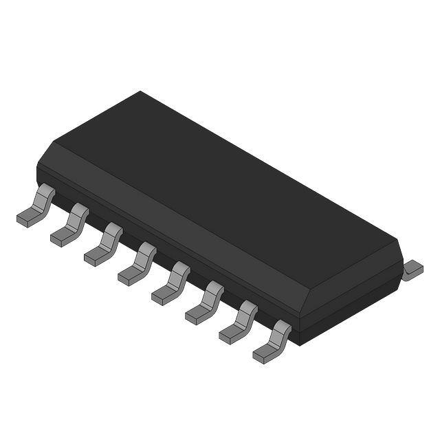
● 16-PIN PLASTIC DIP, SOL-16
APPLICATIONS
● SENSOR AMPLIFIER
THERMOCOUPLE, RTD, BRIDGE
● MEDICAL INSTRUMENTATION
Packages are 16-pin plastic DIP, and SOL-16
surface-mount, specified for the –40°C to +85°C
temperature range.
● MULTIPLE CHANNEL SYSTEMS
V+
–
VINA
G = 10
or
100
1
Over-Voltage
Protection
3
252Ω
4
5050Ω
252Ω
2
Over-Voltage
Protection
–
16
Over-Voltage
Protection
VINB
G = 10
or
100
+
VINB
14
252Ω
13
5050Ω
252Ω
15
INA2141
7
A1A
40kΩ
40kΩ
25kΩ
+
VINA
9
A3A
6
VOA
25kΩ
5
A2A
40kΩ
40kΩ
40kΩ
40kΩ
Ref
10
A1B
25kΩ
A3B
11
VOB
25kΩ
Over-Voltage
Protection
12
A2B
40kΩ
Ref
40kΩ
8
V–
International Airport Industrial Park • Mailing Address: PO Box 11400, Tucson, AZ 85734 • Street Address: 6730 S. Tucson Blvd., Tucson, AZ 85706 • Tel: (520) 746-1111 • Twx: 910-952-1111
Internet: http://www.burr-brown.com/ • FAXLine: (800) 548-6133 (US/Canada Only) • Cable: BBRCORP • Telex: 066-6491 • FAX: (520) 889-1510 • Immediate Product Info: (800) 548-6132
©1995 Burr-Brown Corporation
SBOS036
PDS-1244C
Printed in U.S.A. January, 1996
�SPECIFICATIONS
At TA = +25°C, VS = ±15V, and RL = 10kΩ, unless otherwise noted.
INA2141P, U
PARAMETER
CONDITIONS
INPUT
Offset Voltage, RTI
vs Temperature
vs Power Supply
Long-Term Stability
Safe Input Voltage
Common-Mode Rejection
TYP
MAX
±50
±100
±0.5
±2
±2
±10
(V+) – 2
(V–) + 2
±20
±50
±0.2
±0.5
±1
±2
0.2
0.5
1010 || 2
1010 || 9
(V+) – 1.4
(V–) + 1.7
117
97
125
106
G = 100
G = 10
G = 100
G = 10(2)
VS = ±2.25 to ±18V, G = 100
G = 10
G = 100
G = 10
Impedance, Differential
Common-Mode
Common-Mode Voltage Range(1)
VO = 0V
VCM = ±13V, ∆RS = 1kΩ
G = 100
G = 10
±2
±30
±1
±30
BIAS CURRENT
vs Temperature
Offset Current
vs Temperature
NOISE VOLTAGE, RTI
f = 10Hz
f = 100Hz
f = 1kHz
fB = 0.1Hz to 10Hz
f = 10Hz
f = 100Hz
f = 1kHz
fB = 0.1Hz to 10Hz
Noise Current
f = 10Hz
f = 1kHz
fB = 0.1Hz to 10Hz
GAIN
Gain Error
Gain vs Temperature(2)
Nonlinearity
G = 100, RS = 0Ω
G = 10, RS = 0Ω
VO = ±13.6V, G = 100
G = 10
G = 10, 100
G = 100
G = 10
OUTPUT
Voltage: Positive
Negative
Load Capacitance Stability
Short-Circuit Current
FREQUENCY RESPONSE
Bandwidth, –3dB
RL = 10kΩ
RL = 10kΩ
Overload Recovery
G = 100
G = 10
VO = ±10V, G = 10
VO = ±5V, G = 100
G = 10
50% Overdrive
POWER SUPPLY
Voltage Range
Current, Total
VIN = 0V
Slew Rate
Settling Time, 0.01%
TEMPERATURE RANGE
Specification
Operating
θJA
INA2141PA, UA
MIN
TYP
MAX
UNITS
±125
±250
±1.5
±5
±5
±20
✻
✻
✻
✻
✻
✻
✻
✻
✻
✻
✻
✻
✻
✻
µV
µV
µV/°C
µV/°C
µV/V
µV/V
µV/mo
µV/mo
Ω || pF
Ω || pF
V
V
V
110
93
120
100
±40
✻
±5
✻
✻
✻
✻
±5
±10
±10
nA
pA/°C
nA
pA/°C
✻
✻
✻
✻
✻
✻
✻
✻
nV/√Hz
nV/√Hz
nV/√Hz
µVp-p
nV/√Hz
nV/√Hz
nV/√Hz
µVp-p
0.9
0.3
30
✻
✻
✻
pA/√Hz
pA/√Hz
pAp-p
±0.075
±0.05
±10
±0.002
±0.001
✻
✻
✻
✻
✻
✻
✻
(V+) – 0.9
(V–) + 0.9
1000
+6/–15
200
1
4
9
7
4
±2.25
dB
dB
10
8
8
0.2
22
13
12
0.6
±0.03
±0.01
±2
±0.0005
±0.0003
(V+) – 1.4
(V–) + 1.4
MIN
±15
±1.5
–40
–40
±18
±1.6
✻
85
125
✻
✻
80
±0.15
±0.15
✻
±0.004
±0.002
%
%
ppm/°C
% of FSR
% of FSR
✻
✻
✻
✻
V
V
pF
mA
✻
✻
✻
✻
✻
✻
kHz
MHz
V/µs
µs
µs
µs
✻
✻
✻
✻
✻
V
mA
✻
✻
°C
°C
°C/W
✻ Specification same as INA2141P, U.
NOTE: (1) Input common-mode range varies with output voltage—see typical curves. (2) Guaranteed by wafer test.
The information provided herein is believed to be reliable; however, BURR-BROWN assumes no responsibility for inaccuracies or omissions. BURR-BROWN assumes
no responsibility for the use of this information, and all use of such information shall be entirely at the user’s own risk. Prices and specifications are subject to change
without notice. No patent rights or licenses to any of the circuits described herein are implied or granted to any third party. BURR-BROWN does not authorize or warrant
any BURR-BROWN product for use in life support devices and/or systems.
®
INA2141
2
�PIN CONFIGURATION
Top View
ELECTROSTATIC
DISCHARGE SENSITIVITY
DIP
SOL-16
–
VINA
1
–
16 VINB
+
VINA
2
+
15 VINB
JA
3
14 JB
JA
4
13 JB
RefA
5
12 RefB
VOA
6
11 VOB
SenseA
7
10 SenseB
V–
8
9
This integrated circuit can be damaged by ESD. Burr-Brown
recommends that all integrated circuits be handled with
appropriate precautions. Failure to observe proper handling
and installation procedures can cause damage.
ESD damage can range from subtle performance degradation
to complete device failure. Precision integrated circuits may
be more susceptible to damage because very small parametric
changes could cause the device not to meet its published
specifications.
V+
ORDERING INFORMATION
ABSOLUTE MAXIMUM RATINGS
Supply Voltage .................................................................................. ±18V
Analog Input Voltage Range ............................................................. ±40V
Output Short-Circuit (to ground) .............................................. Continuous
Operating Temperature ................................................. –40°C to +125°C
Storage Temperature ..................................................... –40°C to +125°C
Junction Temperature .................................................................... +150°C
Lead Temperature (soldering, 10s) ............................................... +300°C
PRODUCT
PACKAGE
PACKAGE
DRAWING
NUMBER(1)
INA2141PA
INA2141P
INA2141UA
INA2141U
16-Pin Plastic DIP
16-Pin Plastic DIP
SOL-16 Surface-Mount
SOL-16 Surface-Mount
180
180
211
211
TEMPERATURE
RANGE
–40°C to +85°C
–40°C to +85°C
–40°C to +85°C
–40°C to +85°C
NOTE: (1) For detailed drawing and dimension table, please see end of data
sheet, or Appendix C of Burr-Brown IC Data Book.
®
3
INA2141
�TYPICAL PERFORMANCE CURVES
At TA = +25°C, and VS = ±15V, unless otherwise noted.
COMMON-MODE REJECTION vs FREQUENCY
GAIN vs FREQUENCY
60
140
Common-Mode Rejection (dB)
50
40
Gain (dB)
G = 100V/V
30
20
G = 10V/V
10
0
–10
–20
G = 10V/V
100
80
60
40
20
0
1k
10k
100k
1M
10M
10
100
1k
100k
10k
Frequency (Hz)
Frequency (Hz)
POSITIVE POWER SUPPLY REJECTION
vs FREQUENCY
NEGATIVE POWER SUPPLY REJECTION
vs FREQUENCY
140
140
120
120
100
Power Supply Rejection (dB)
Power Supply Rejection (dB)
G = 100V/V
120
G = 100V/V
80
60
G = 10V/V
40
1M
G = 100V/V
100
80
60
40
G = 10V/V
20
20
0
0
10
100
1k
10k
100k
10
1M
100
1k
10k
100k
Frequency (Hz)
Frequency (Hz)
INPUT COMMON-MODE RANGE
vs OUTPUT VOLTAGE, VS = ±15V
INPUT COMMON-MODE RANGE
vs OUTPUT VOLTAGE, VS = ±5, ±2.5V
15
1M
5
Common-Mode Voltage (V)
Common-Mode Voltage (V)
4
10
5
VD/2
0
VD/2
+
–5
VCM
+15V
–
VO
+
–
Ref
+
–15V
–10
3
2
1
0
–1
–2
–3
VS = ±5V
VS = ±2.5V
–4
–15
–15
–10
–5
0
5
10
–5
–5
15
Output Voltage (V)
–3
–2
–1
0
1
Output Voltage (V)
®
INA2141
–4
4
2
3
4
5
�TYPICAL PERFORMANCE CURVES
(CONT)
At TA = +25°C, and VS = ±15V, unless otherwise noted.
CROSSTALK vs FREQUENCY
INPUT- REFERRED NOISE vs FREQUENCY
G = 100V/V
120
G = 10V/V
Crosstalk (dB)
100
80
60
40
20
0
100
1k
10
100
G = 10V/V
1
10
G = 100
Current Noise
0.1
1
10
100
1k
10k
100k
1M
Input Bias Current Noise (pA/√ Hz)
Input-Referred Voltage Noise (nV/√ Hz)
140
1
10
100
Frequency (Hz)
1k
10k
Frequency (Hz)
QUIESCENT CURRENT and SLEW RATE
vs TEMPERATURE
INPUT OVER-VOLTAGE V/I CHARACTERISTICS
1.8
6
1.7
5
5
4
Slew Rate
1.5
3
IQ
1.4
Input Current (mA)
1.6
3
Slew Rate (V/µs)
Quiescent Current (µA)
4
Flat region represents
normal linear operation.
2
G = 10V/V
0
–1
+15V
G = 10V/V
–2
–3
2
G = 100V/V
1
1/2
INA2141
G = 100V/V
VIN
–4
1.3
–75
–50
–25
0
25
50
75
100
IIN
–15V
–5
1
125
–50 –40 –30
–20 –10
0
10
20
30
40
50
Input Voltage (V)
Temperature (°C)
INPUT BIAS CURRENT vs TEMPERATURE
OFFSET VOLTAGE WARM-UP
2
10
G = 100V/V
6
Input Bias Current (nA)
Offset Voltage Change (µV)
8
4
2
0
–2
–4
IB
1
IOS
0
Typical IB and IOS
Range ±2nA at 25°C
–1
–6
–8
–2
–10
0
10
20
30
40
50
–75
Time (ms)
–50
–25
0
25
50
75
100
125
Temperature (°C)
®
5
INA2141
�TYPICAL PERFORMANCE CURVES
(CONT)
At TA = +25°C, and VS = ±15V, unless otherwise noted.
OUTPUT VOLTAGE SWING
vs POWER SUPPLY VOLTAGE
V+
(V+)–0.4
(V+)–0.4
Output Voltage Swing (V)
(V+)
(V+)–0.8
(V+)–1.2
(V+)+1.2
(V–)+0.8
+25°C +85°C
(V+)–0.8
–40°C
(V+)–1.2
RL = 10kΩ
(V–)+1.2
+25°C
–40°C
(V–)+0.8
(V–)+0.4
(V–)+0.4
+85°C
–40°C
0
1
2
3
0
4
Output Current (mA)
5
10
15
20
Power Supply Voltage (V)
SHORT-CIRCUIT OUTPUT CURRENT
vs TEMPERATURE
MAXIMUM OUTPUT VOLTAGE vs FREQUENCY
30
16
Peak-to-Peak Output Voltage (Vpp)
–ISC
14
Short Circuit Current (mA)
+85°C
V–
V–
12
10
8
6
4
+ISC
2
G = 10, 100
25
20
15
10
5
0
0
–75
–50
–25
0
25
50
75
100
1k
125
10k
100k
1M
Frequency (Hz)
Temperature (°C)
VOLTAGE NOISE 0.1 to 10Hz
INPUT-REFERRED, G = 100
TOTAL HARMONIC DISTORTION + NOISE
vs FREQUENCY
1
VO = 1Vrms
500kHz Measurement
Bandwidth
THD+N (%)
Output Voltage (V)
OUTPUT VOLTAGE SWING
vs OUTPUT CURRENT
0.1
RL = 10kΩ
G = 100, RL = 100kΩ
0.1µV/div
0.01
G = 10V/V
RL = 100kΩ
Dashed Portion
is noise limited.
0.001
100
1k
10k
100k
1s/div
Frequency (Hz)
®
INA2141
6
�TYPICAL PERFORMANCE CURVES
(CONT)
At TA = +25°C, and VS = ±15V unless otherwise noted.
SMALL-SIGNAL STEP RESPONSE
LARGE-SIGNAL STEP RESPONSE
G = 10
G = 10
20mV/div
5V/div
G = 100
G = 100
5µs/div
5µs/div
®
7
INA2141
�APPLICATION INFORMATION
Internal resistor ratios are laser trimmed to assure excellent
gain accuracy. Actual resistor values can vary by approximately ±25% from the nominal values shown.
Figure 1 shows the basic connections required for operation
of the INA2141. Applications with noisy or high impedance
power supplies may require decoupling capacitors close to
the device pins as shown.
Gains between 10 and 100 can be achieved by connecting an
external resistor to the jumper pins. This is not recommended, however, because the ±25% variation of internal
resistor values makes the required external resistor value
uncertain. A companion model, INA2128, features accurately trimmed internal resistors so that gains from 1 to
10,000 can be set with an external resistor.
The output is referred to the output reference (Ref) terminals
(RefA and RefB) which are normally grounded. These must
be low-impedance connections to assure good commonmode rejection. A resistance of 8Ω in series with a Ref pin
will cause a typical device to degrade to approximately
80dB CMR (G = 1).
The INA2141 has a separate output sense feedback connections SenseA and SenseB. These must be connected to their
respective output terminals for proper operation. The output
sense connection can be used to sense the output voltage
directly at the load for best accuracy.
DYNAMIC PERFORMANCE
The typical performance curve “Gain vs Frequency” shows
that despite its low quiescent current, the INA2141 achieves
wide bandwidth, even at high gain. This is due to its currentfeedback topology. Settling time also remains excellent at
high gain.
SETTING THE GAIN
Gain of each IA can be independently selected with a jumper
connection as shown in Figure 1. G = 10V/V with no jumper
installed. With a jumper installed G = 100V/V. To preserve
good gain accuracy, this jumper must have low series
resistance. A resistance of 0.5Ω in series with the jumper
will decrease the gain by 0.1%.
NOISE PERFORMANCE
The INA2141 provides very low noise in most applications.
Low frequency noise is approximately 0.2µVp-p measured
from 0.1 to 10Hz (G = 100). This provides dramatically
improved noise when compared to state-of-the-art chopperstabilized amplifiers.
V+
0.1µF
Pin numbers for
Channel B shown
in parenthesis.
–
VIN
G = 10V/V
Open Circuit
J
1
(16)
9
INA2141
Over-Voltage
Protection
40kΩ
3
(14)
252Ω
+
VIN
(13)
2
(15)
6
(11)
A3
25kΩ
Load VO
252Ω
–
Ref
A2
Over-Voltage
Protection
40kΩ
8
40kΩ
5
(12)
0.1µF
V–
Also drawn in simplified form:
–
VIN
INA2141
+
VIN
VO
Ref
FIGURE 1. Basic Connections.
®
INA2141
+
–
)
VO = G • (VIN – VIN
+
4
J
40kΩ
25kΩ
5050Ω
G = 100V/V
Connect Jumper
7 Sense
(10)
A1
8
NOTE: If channel is unused,
connect inputs to ground, sense
to VO, and leave Ref open-circuit.
�OFFSET TRIMMING
The INA2141 is laser trimmed for low offset voltage and
offset voltage drift. Most applications require no external
offset adjustment. Figure 2 shows an optional circuit for
trimming the output offset voltage. The voltage applied to
Ref terminal is summed with the output. The op amp buffer
provides low impedance at the Ref terminal to preserve good
common-mode rejection.
–
VIN
VO
1/2
INA2141
47kΩ
V+
1/2
INA2141
V+
Microphone,
Hydrophone
etc.
47kΩ
1/2
INA2141
Thermocouple
100µA
1/2 REF200
Ref
IN
10kΩ
OPA177
10kΩ
100Ω
(For other
channel)
±10mV
Adjustment Range
1/2
INA2141
100Ω
100µA
1/2 REF200
Center-tap provides
bias current return.
V–
FIGURE 2. Optional Trimming of Output Offset Voltage.
FIGURE 3. Providing an Input Common-Mode Current Path.
INPUT BIAS CURRENT RETURN PATH
The input impedance of the INA2141 is extremely high—
approximately 1010Ω. However, a path must be provided for
the input bias current of both inputs. This input bias current
is approximately ±2nA. High input impedance means that
this input bias current changes very little with varying input
voltage.
mon-mode input range is related to the output voltage of the
complete amplifier. This behavior also depends on supply
voltage—see performance curves “Input Common-Mode
Range vs Output Voltage”.
Input-overload can produce an output voltage that appears
normal. For example, if an input overload condition drives
both input amplifiers to their positive output swing limit, the
difference voltage measured by the output amplifier will be
near zero. The output of the INA2141 will be near 0V even
though both inputs are overloaded.
Input circuitry must provide a path for this input bias current
for proper operation. Figure 3 shows various provisions for
an input bias current path. Without a bias current path, the
inputs will float to a potential which exceeds the commonmode range of the INA2141 and the input amplifiers will
saturate.
LOW VOLTAGE OPERATION
The INA2141 can be operated on power supplies as low as
±2.25V. Performance remains excellent with power supplies ranging from ±2.25V to ±18V. Most parameters vary
only slightly throughout this supply voltage range—see
typical performance curves. Operation at very low supply
voltage requires careful attention to assure that the input
voltages remain within their linear range. Voltage swing
requirements of internal nodes limit the input commonmode range with low power supply voltage. Typical performance curves, “Input Common-Mode Range vs Output
Voltage” show the range of linear operation for ±15V, ±5V,
and ±2.5V supplies.
If the differential source resistance is low, the bias current
return path can be connected to one input (see the thermocouple example in Figure 3). With higher source impedance,
using two equal resistors provides a balanced input with
possible advantages of lower input offset voltage due to bias
current and better high-frequency common-mode rejection.
INPUT COMMON-MODE RANGE
The linear input voltage range of the input circuitry of the
INA2141 is from approximately 1.4V below the positive
supply voltage to 1.7V above the negative supply. As a
differential input voltage causes the output voltage increase,
however, the linear input range will be limited by the output
voltage swing of amplifiers A1 and A2. So the linear com-
®
9
INA2141
�INPUT PROTECTION
The inputs of the INA2141 are individually protected for
voltages up to ±40V. For example, a condition of –40V on
one input and +40V on the other input will not cause
damage. Internal circuitry on each input provides low series
impedance under normal signal conditions. To provide
equivalent protection, series input resistors would contribute
excessive noise. If the input is overloaded, the protection
circuitry limits the input current to a safe value of approximately 1.5 to 5mA. The typical performance curve “Input
Bias Current vs Common-Mode Input Voltage” shows this
input current limit behavior. The inputs are protected even if
the power supplies are disconnected or turned off.
there is virtually no signal coupling between channels.
Crosstalk increases with frequency and is dependent on
circuit gain, source impedance and signal characteristics.
As source impedance increases, careful circuit layout will
help achieve lowest channel crosstalk. Most crossstalk is
produced by capacitive coupling of signals from one channel
to the input section of the other channel. To minimize
coupling, separate the input traces as far as practical from
any signals associated with the opposite channel. A grounded
guard trace surrounding the inputs helps reduce stray coupling between channels. Run the differential inputs of each
channel parallel to each other or directly adjacent on top and
bottom side of a circuit board. Stray coupling then tends to
produce a common-mode signal which is rejected by the
IA’s input.
CHANNEL CROSSTALK
The two channels of the INA2141 are completely independent, including all bias circuitry. At DC and low frequency
VEX
X-axis
1/2
INA2141
V1
X-axis
VO
VO = 10 (V2 – V1) + 10 (V4 – V3)
1/2
INA2141
Ref
V2
VEX
V3
1/2
INA2141
Y-axis
Ref
1/2
INA2141
V4
Y-axis
VO
FIGURE 4. Two-Axis Bridge Amplifier.
FIGURE 5. Sum of Differences Amplifier.
1/4
OPA4131
1/2
INA2141
1/4
OPA4131
LA
RA
20kΩ
390kΩ
1/4
OPA4131
RL
VG
1/4
OPA4131
10kΩ
390kΩ
FIGURE 6. ECG Amplifier With Right-Leg Drive.
®
INA2141
10
VO
Ref
G = 10
20kΩ
�PACKAGE OPTION ADDENDUM
www.ti.com
7-Oct-2021
PACKAGING INFORMATION
Orderable Device
Status
(1)
Package Type Package Pins Package
Drawing
Qty
Eco Plan
(2)
Lead finish/
Ball material
MSL Peak Temp
Op Temp (°C)
Device Marking
(3)
(4/5)
(6)
INA2141U
ACTIVE
SOIC
DW
16
40
RoHS & Green
Call TI
Level-3-260C-168 HR
-40 to 85
INA2141UA
ACTIVE
SOIC
DW
16
40
RoHS & Green
Call TI
Level-3-260C-168 HR
INA2141U
A
INA2141UA/1K
ACTIVE
SOIC
DW
16
1000
RoHS & Green
Call TI
Level-3-260C-168 HR
INA2141U
A
INA2141UE4
ACTIVE
SOIC
DW
16
40
RoHS & Green
Call TI
Level-3-260C-168 HR
-40 to 85
INA2141U
A
INA2141U
A
(1)
The marketing status values are defined as follows:
ACTIVE: Product device recommended for new designs.
LIFEBUY: TI has announced that the device will be discontinued, and a lifetime-buy period is in effect.
NRND: Not recommended for new designs. Device is in production to support existing customers, but TI does not recommend using this part in a new design.
PREVIEW: Device has been announced but is not in production. Samples may or may not be available.
OBSOLETE: TI has discontinued the production of the device.
(2)
RoHS: TI defines "RoHS" to mean semiconductor products that are compliant with the current EU RoHS requirements for all 10 RoHS substances, including the requirement that RoHS substance
do not exceed 0.1% by weight in homogeneous materials. Where designed to be soldered at high temperatures, "RoHS" products are suitable for use in specified lead-free processes. TI may
reference these types of products as "Pb-Free".
RoHS Exempt: TI defines "RoHS Exempt" to mean products that contain lead but are compliant with EU RoHS pursuant to a specific EU RoHS exemption.
Green: TI defines "Green" to mean the content of Chlorine (Cl) and Bromine (Br) based flame retardants meet JS709B low halogen requirements of


 工商网监
湘ICP备2023018690号
工商网监
湘ICP备2023018690号
