User's Guide
SBOU177A – September 2016 – Revised July 2017
INA240EVM User's Guide
This user’s guide describes the characteristics, operation, and use of the INA240EVM evaluation module.
This guide discusses how to set up and configure the hardware. Throughout this document, the terms
evaluation board, evaluation module, and EVM are synonymous with the INA240EVM. This document
includes an electrical schematic, printed circuit board (PCB) layout drawings, and a parts list for the EVM.
1
2
3
Contents
Overview .....................................................................................................................
1.1
INA240EVM Kit Contents ..........................................................................................
1.2
Related Documentation from Texas Instruments ...............................................................
INA240EVM Hardware ......................................................................................................
2.1
Theory of Operation for the INA240EVM ........................................................................
2.2
INA240EVM Features ..............................................................................................
2.3
Quick-Start Setup and Use ........................................................................................
2.4
Voltage Inputs .......................................................................................................
2.5
Setting the Reference ..............................................................................................
Schematic, PCB Layout, and Bill of Materials ...........................................................................
3.1
Schematic ............................................................................................................
3.2
PCB Layout ..........................................................................................................
3.3
Bill of Materials ......................................................................................................
2
2
2
3
3
3
4
4
4
5
5
6
7
List of Figures
1
INA240EVM Test Board Block Diagram .................................................................................. 3
2
INA240EVM Test Board Schematic ....................................................................................... 5
3
INA240EVM Component Placement ...................................................................................... 6
SBOU177A – September 2016 – Revised July 2017
Submit Documentation Feedback
Copyright © 2016–2017, Texas Instruments Incorporated
INA240EVM User's Guide
1
�Overview
www.ti.com
4
PCB Top Layer ............................................................................................................... 6
5
PCB Bottom Layer ........................................................................................................... 6
List of Tables
1
INA240EVM Kit Contents ................................................................................................... 2
2
INA240 Test Board BOM
..................................................................................................
7
Trademarks
All trademarks are the property of their respective owners.
1
Overview
The INA240 device is a voltage output current shunt monitor that senses drops across shunts at specified
common-mode voltages from –4 V to 80 V, independent of the supply voltage.
NOTE: This EVM limits the maximum common-mode voltage to 70 V with clamping diodes D1 and
D2.
Remove D1 and D2 when test input signal is non-DC.
The device operates from a single 2.7-V to 5.5-V power supply, drawing a typical supply current of
approximately 1 mA. The INA240EVM package includes one large PCB that can be broken apart into four
separate PCBs, one for each of the four gain versions (INA240A1/A2/A3/A4). The EVM includes test
points for external hardware connections, placeholder pads to add filtering components, and surfacemount resistors for ease of setting the reference.
1.1
INA240EVM Kit Contents
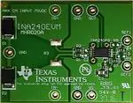
Table 1 lists the contents of the INA240EVM kit. The included hardware is pictured on the front page that
shows only one of the four INA240 devices and the associated EVM hardware. Contact the nearest Texas
Instruments Product Information Center if any component is missing. Take care to check the INA240
Product Folder on the TI web site at www.ti.com for any further information regarding this product.
Table 1. INA240EVM Kit Contents
1.2
ITEM
QUANTITY
INA240A1 EVM test board
1
INA240A2 EVM test board
1
INA240A3 EVM test board
1
INA240A4 EVM test board
1
Related Documentation from Texas Instruments
The following documents provide information regarding Texas Instruments' integrated circuits used in the
assembly of the INA240EVM. This user's guide is available from the TI web site under literature number
SBOU177. Any letter appended to the literature number corresponds to the document revision that is
current at the time of the writing of this document. Newer revisions may be available from the TI web site
(www.ti.com), or by calling the Texas Instruments' Literature Response Center at (800) 477-8924 or the
Product Information Center at (972) 644-5580. When ordering, identify the document by title and literature
number.
For related documentation, refer to INA240 Wide Common-Mode Range, Voltage Output, High- or LowSide Bidirectional, Zero-Drift, Current-Shunt Monitor (SBOS662)
2
INA240EVM User's Guide
SBOU177A – September 2016 – Revised July 2017
Submit Documentation Feedback
Copyright © 2016–2017, Texas Instruments Incorporated
�INA240EVM Hardware
www.ti.com
2
INA240EVM Hardware
The INA240EVM requires a 2.7-V to 5.5-V power supply. Connect the VIN+ and VIN– pins across an
external shunt resistor in series with a –4-V to 70-V supply to determine the current flowing through the
resistor. Use a voltmeter on the OUT pin to measure the voltage output. The REF1 and REF2 pins set the
output reference.
2.1
Theory of Operation for the INA240EVM
A block diagram of the INA240EVM test board hardware is shown in Figure 1. The INA240 test board
contains test points that provide access to all eight pins of the INA240 device for evaluation. A footprint is
provided for the input filtering circuitry. The REF1 and REF2 pins are equipped with jumpers to set the
output reference to VS, GND, half VS, or any desired external reference level.
INA240A1/2/3/4
GND
OUT
VS
IN+
REF1
IN±
REF2
VS
GND
VS
Copyright © 2017, Texas Instruments Incorporated
Figure 1. INA240EVM Test Board Block Diagram
2.2
INA240EVM Features
The INA240EVM provides a basic functional evaluation of the INA240. The fixture layout is not intended to
be a model for the target circuit, or laid out for electromagnetic compatibility (EMC) testing.
The layout of the INA240EVM printed circuit board (PCB) provides the following features:
• Simple access to all device pins
• Multiple input signal options
• Space for optional input filtering
• Configurable reference pins
The INA240EVM connects to both sides of a remote shunt resistor to measure current, or omits the shunt
resistor and applies a differential voltage directly to the device inputs. This flexibility allows the testing of
device operation in a simulated manner and an actual application.
See INA240 Wide Common-Mode Range, Voltage Output, High- or Low-Side Bidirectional, Zero-Drift,
Current-Shunt Monitor (SBOS662) for comprehensive information about the INA240 family.
SBOU177A – September 2016 – Revised July 2017
Submit Documentation Feedback
Copyright © 2016–2017, Texas Instruments Incorporated
INA240EVM User's Guide
3
�INA240EVM Hardware
2.3
www.ti.com
Quick-Start Setup and Use
Follow the procedure listed below to set up and use the INA240EVM:
1. Connect an external dc supply voltage between 2.7-V and 5.5-V to the VS test point.
2. Connect the desired input to input test points, IN+ and IN-. This input is a remote shunt resistor or a
differential voltage source with a common-mode voltage of –4 V to 70 V referenced to GND. Note that
the INA240 device has a rated common-mode voltage of 80 V, however the full 80 V is unavailable on
the EVM because the input is limited by the D1 and D2 clamping diodes.
2.4
Voltage Inputs
The IN+ and IN– test points connect to a remote shunt resistor or a differential voltage source. The
voltage differential is multiplied by the device gain of the INA240 device. There are four devices in this
family, which include: the INA240A1 with 20-V/V gain, the INA240A2 with 50-V/V gain, the INA240A3 with
100-V/V gain, and the INA240A4 with 200-V/V gain. The full-scale sense input voltage (VSENSE) is defined
as VIN+ – VIN–, and has a maximum input of (V+ – 0.20) per gain to achieve linear output. The minimum
voltage output is 10 mV.
2.5
Setting the Reference
The INA240 output is referenced to the voltage level defined by the REF1 and REF2 pins. The two
reference pins independently connect to VS, GND, or an external source. It is possible to set the reference
level to VS, GND, half VS, or an arbitrary level through external sources.
4
INA240EVM User's Guide
SBOU177A – September 2016 – Revised July 2017
Submit Documentation Feedback
Copyright © 2016–2017, Texas Instruments Incorporated
�Schematic, PCB Layout, and Bill of Materials
www.ti.com
3
Schematic, PCB Layout, and Bill of Materials
3.1
Schematic
Figure 2 shows the complete schematic of the INA240 test board. Only the EVM associated with
INA240A1 is shown. C1 and C3 are bypass capacitors for VS. C2, R1, and R2 create an optional filter for
the VIN+ and VIN– inputs. R3 is an optional shunt resistor for the INA input. R4 through R7 are jumpers
that enable the flexibility in configuring the reference level. The reference is set by splitting VS by default.
D1 and D2 are clamps that limit the maximum common-mode voltage to 70 V, although the INA240 is
rated at 80 V.
Figure 2. INA240EVM Test Board Schematic
SBOU177A – September 2016 – Revised July 2017
Submit Documentation Feedback
Copyright © 2016–2017, Texas Instruments Incorporated
INA240EVM User's Guide
5
�Schematic, PCB Layout, and Bill of Materials
3.2
www.ti.com
PCB Layout
Figure 3 shows the component placement on the INA240EVM test board. There are no components on
the bottom layer. Figure 4 and Figure 5 show the top and bottom layers of the test board, respectively.
Figure 3. INA240EVM Component Placement
Figure 4. PCB Top Layer
6
INA240EVM User's Guide
Figure 5. PCB Bottom Layer
SBOU177A – September 2016 – Revised July 2017
Submit Documentation Feedback
Copyright © 2016–2017, Texas Instruments Incorporated
�Schematic, PCB Layout, and Bill of Materials
www.ti.com
3.3
Bill of Materials
Table 2 lists the bill of materials (BOM) for the INA240 test board, which includes four identical PCBs, one
for each of the gain versions in the INA240 family.
Table 2. INA240 Test Board BOM
QUANTI
TY
REFDES
DESCRIPTION
PART NUMBER
MANUFACTURER
4
C1
CAP, CERM, 0.1 µF, 16 V, +/- 5%, X7R, 0603
0603YC104JAT2A
AVX
4
C3
CAP, CERM, 1 µF, 25 V, +/- 10%, X5R, 0805
08053D105KAT2A
AVX
8
D1, D2
Diode, TVS, Uni, 70 V, 600 W, SMB
SMBJ70A-13-F
Diodes Inc.
RES, 0, 5%, 0.1 W, 0603
ERJ-3GEY0R00V
Panasonic
Bumpon, Hemisphere, 0.44 × 0.20, Clear
SJ-5303 (CLEAR)
3M
16
R1, R2, R4, R7
16
H9,H10,H11,H12
1
U1
Wide Common-Mode Range, Voltage Output, High or Low-Side BiDirectional Zero-Drift Current Shunt Monitor, PW0008A
INA240A1PW
ERJ-6GEY0R00V
1
U2
Wide Common-Mode Range, Voltage Output, High or Low-Side BiDirectional Zero-Drift Current Shunt Monitor, PW0008A
INA240A2PW
Texas Instruments
1
U3
Wide Common-Mode Range, Voltage Output, High or Low-Side BiDirectional Zero-Drift Current Shunt Monitor, PW0008A
INA240A3PW
Texas Instruments
1
U4
Wide Common-Mode Range, Voltage Output, High or Low-Side BiDirectional Zero-Drift Current Shunt Monitor, PW0008A
INA240A4PW
Texas Instruments
SBOU177A – September 2016 – Revised July 2017
Submit Documentation Feedback
Copyright © 2016–2017, Texas Instruments Incorporated
INA240EVM User's Guide
7
�Revision History
www.ti.com
Revision History
NOTE: Page numbers for previous revisions may differ from page numbers in the current version.
Changes from Original (September 2016) to A Revision ............................................................................................... Page
•
8
Added note to remove D1 and D2 for non-DC test input signal
Revision History
....................................................................
2
SBOU177A – September 2016 – Revised July 2017
Submit Documentation Feedback
Copyright © 2016–2017, Texas Instruments Incorporated
�IMPORTANT NOTICE FOR TI DESIGN INFORMATION AND RESOURCES
Texas Instruments Incorporated (‘TI”) technical, application or other design advice, services or information, including, but not limited to,
reference designs and materials relating to evaluation modules, (collectively, “TI Resources”) are intended to assist designers who are
developing applications that incorporate TI products; by downloading, accessing or using any particular TI Resource in any way, you
(individually or, if you are acting on behalf of a company, your company) agree to use it solely for this purpose and subject to the terms of
this Notice.
TI’s provision of TI Resources does not expand or otherwise alter TI’s applicable published warranties or warranty disclaimers for TI
products, and no additional obligations or liabilities arise from TI providing such TI Resources. TI reserves the right to make corrections,
enhancements, improvements and other changes to its TI Resources.
You understand and agree that you remain responsible for using your independent analysis, evaluation and judgment in designing your
applications and that you have full and exclusive responsibility to assure the safety of your applications and compliance of your applications
(and of all TI products used in or for your applications) with all applicable regulations, laws and other applicable requirements. You
represent that, with respect to your applications, you have all the necessary expertise to create and implement safeguards that (1)
anticipate dangerous consequences of failures, (2) monitor failures and their consequences, and (3) lessen the likelihood of failures that
might cause harm and take appropriate actions. You agree that prior to using or distributing any applications that include TI products, you
will thoroughly test such applications and the functionality of such TI products as used in such applications. TI has not conducted any
testing other than that specifically described in the published documentation for a particular TI Resource.
You are authorized to use, copy and modify any individual TI Resource only in connection with the development of applications that include
the TI product(s) identified in such TI Resource. NO OTHER LICENSE, EXPRESS OR IMPLIED, BY ESTOPPEL OR OTHERWISE TO
ANY OTHER TI INTELLECTUAL PROPERTY RIGHT, AND NO LICENSE TO ANY TECHNOLOGY OR INTELLECTUAL PROPERTY
RIGHT OF TI OR ANY THIRD PARTY IS GRANTED HEREIN, including but not limited to any patent right, copyright, mask work right, or
other intellectual property right relating to any combination, machine, or process in which TI products or services are used. Information
regarding or referencing third-party products or services does not constitute a license to use such products or services, or a warranty or
endorsement thereof. Use of TI Resources may require a license from a third party under the patents or other intellectual property of the
third party, or a license from TI under the patents or other intellectual property of TI.
TI RESOURCES ARE PROVIDED “AS IS” AND WITH ALL FAULTS. TI DISCLAIMS ALL OTHER WARRANTIES OR
REPRESENTATIONS, EXPRESS OR IMPLIED, REGARDING TI RESOURCES OR USE THEREOF, INCLUDING BUT NOT LIMITED TO
ACCURACY OR COMPLETENESS, TITLE, ANY EPIDEMIC FAILURE WARRANTY AND ANY IMPLIED WARRANTIES OF
MERCHANTABILITY, FITNESS FOR A PARTICULAR PURPOSE, AND NON-INFRINGEMENT OF ANY THIRD PARTY INTELLECTUAL
PROPERTY RIGHTS.
TI SHALL NOT BE LIABLE FOR AND SHALL NOT DEFEND OR INDEMNIFY YOU AGAINST ANY CLAIM, INCLUDING BUT NOT
LIMITED TO ANY INFRINGEMENT CLAIM THAT RELATES TO OR IS BASED ON ANY COMBINATION OF PRODUCTS EVEN IF
DESCRIBED IN TI RESOURCES OR OTHERWISE. IN NO EVENT SHALL TI BE LIABLE FOR ANY ACTUAL, DIRECT, SPECIAL,
COLLATERAL, INDIRECT, PUNITIVE, INCIDENTAL, CONSEQUENTIAL OR EXEMPLARY DAMAGES IN CONNECTION WITH OR
ARISING OUT OF TI RESOURCES OR USE THEREOF, AND REGARDLESS OF WHETHER TI HAS BEEN ADVISED OF THE
POSSIBILITY OF SUCH DAMAGES.
You agree to fully indemnify TI and its representatives against any damages, costs, losses, and/or liabilities arising out of your noncompliance with the terms and provisions of this Notice.
This Notice applies to TI Resources. Additional terms apply to the use and purchase of certain types of materials, TI products and services.
These include; without limitation, TI’s standard terms for semiconductor products http://www.ti.com/sc/docs/stdterms.htm), evaluation
modules, and samples (http://www.ti.com/sc/docs/sampterms.htm).
Mailing Address: Texas Instruments, Post Office Box 655303, Dallas, Texas 75265
Copyright © 2017, Texas Instruments Incorporated
�