Product
Folder
Order
Now
Support &
Community
Tools &
Software
Technical
Documents
INA253
SLOS954A – JULY 2018 – REVISED DECEMBER 2018
INA253 High Voltage, Bidirectional, Zero-Drift, Current-Shunt Monitor
With Integrated, 2-mΩ, Precision, Low Inductive Shunt Resistor
1 Features
3 Description
•
The INA253 is a voltage-output, current sense
amplifier with an integrated shunt resistor of 2 mΩ.
The INA253 is designed to monitor bidirectional
currents over a wide common-mode range from
–4 V to +80 V, independent of the supply voltage.
Three fixed gains are available: 100 mV/A, 200 mV/A,
and 400 mV/A. The integration of the precision
resistor with a zero-drift chopped amplifier provides
calibration equivalent measurement accuracy, ultralow temperature drift performance of 15 ppm/°C, and
an optimized Kelvin layout for the sensing resistor.
1
•
•
•
•
•
•
•
Precision Integrated Shunt Resistor
– Shunt Resistor: 2 mΩ
– Shunt Inductance: 3 nH
– Shunt Resistor Tolerance: 0.1% (Max)
– ±15 A Continuous from –40°C to +85°C
– 0°C to 125°C Temperature Coefficient:
10 ppm/°C
High Bandwidth: 350 kHz
Enhanced PWM rejection
Excellent CMRR
– > 120-dB DC CMRR
– 90-dB AC CMRR at 50 kHz
Accuracy:
– Gain:
– Gain Error: 0.4% (Max)
– Gain Drift: 45 ppm/°C (Max)
– Offset:
– Offset Current: ±15 mA (Max)
– Offset Drift: 125 µA/°C (Max)
Wide Common-Mode Range: –4 V to +80 V
Available Gains: 100 mV/A, 200 mV/A,
and 400 mV/A
Quiescent Current: 2.4 mA (Max)
2 Applications
•
•
•
•
•
•
Solenoid and Valve Controls
Transmission control
Motor Controls
Actuator Controls
DC/DC Converters
Remote I/O Link Control
The INA253 is designed with enhanced PWM
rejection circuitry to suppress large (dv/dt) signals
that
enable
real-time
continuous
current
measurements. The measurements are critical for inline current measurements in a motor-drive
application, and for solenoid valve control
applications.
This device operates from a single 2.7-V to 5.5-V
power supply, drawing a maximum of 3 mA of supply
current. All gain versions are specified over the
extended operating temperature range (–40°C to
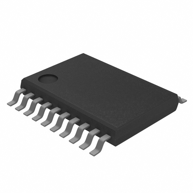
+125°C), and are available in a 20-pin TSSOP
package.
Device Information(1)
PART NUMBER
INA253
PACKAGE
BODY SIZE (NOM)
TSSOP (20)
6.50 mm × 4.40 mm
(1) For all available packages, see the package option addendum
at the end of the data sheet.
Typical Application
Up To 80 V
2.7-V to 5.5-V
Supply
VS
IN+
IN±
REF2
INA253
+
OUT
±
GND
REF1
1
An IMPORTANT NOTICE at the end of this data sheet addresses availability, warranty, changes, use in safety-critical applications,
intellectual property matters and other important disclaimers. PRODUCTION DATA.
�INA253
SLOS954A – JULY 2018 – REVISED DECEMBER 2018
www.ti.com
Table of Contents
1
2
3
4
5
6
7
8
Features ..................................................................
Applications ...........................................................
Description .............................................................
Revision History.....................................................
Device Comparison Table.....................................
Pin Configuration and Functions .........................
Specifications.........................................................
1
1
1
2
3
3
4
7.1
7.2
7.3
7.4
7.5
7.6
4
4
4
4
5
7
Absolute Maximum Ratings ......................................
ESD Ratings..............................................................
Recommended Operating Conditions.......................
Thermal Information ..................................................
Electrical Characteristics...........................................
Typical Characteristics ..............................................
Detailed Description ............................................ 12
8.1 Overview ................................................................. 12
8.2 Functional Block Diagram ....................................... 12
8.3 Feature Description................................................. 12
8.4 Device Functional Modes........................................ 16
9
Application and Implementation ........................ 19
9.1 Application Information............................................ 19
9.2 Typical Applications ............................................... 21
10 Power Supply Recommendations ..................... 27
11 Layout................................................................... 27
11.1 Layout Guidelines ................................................. 27
11.2 Layout Example .................................................... 27
12 Device and Documentation Support ................. 28
12.1
12.2
12.3
12.4
12.5
12.6
12.7
Device Support......................................................
Related Documentation .......................................
Receiving Notification of Documentation Updates
Community Resources..........................................
Trademarks ...........................................................
Electrostatic Discharge Caution ............................
Glossary ................................................................
28
28
28
28
28
28
28
13 Mechanical, Packaging, and Orderable
Information ........................................................... 28
4 Revision History
Changes from Original (July 2018) to Revision A
•
2
Page
Changed device status from advanced information to production data (active) .................................................................... 1
Submit Documentation Feedback
Copyright © 2018, Texas Instruments Incorporated
Product Folder Links: INA253
�INA253
www.ti.com
SLOS954A – JULY 2018 – REVISED DECEMBER 2018
5 Device Comparison Table
PRODUCT
GAIN (mV/A)
INA253A1
100
INA253A2
200
INA253A3
400
6 Pin Configuration and Functions
PW Package
20-Pin TSSOP
Top View
IS±
1
20
IS+
IS±
2
19
IS+
IS±
3
18
IS+
SH±
4
17
SH+
IN±
5
16
IN+
GND
6
15
NC
DNC1
7
14
DNC2
NC
8
13
OUT
VS
9
12
NC
10
11
REF1
REF2
Not to scale
Pin Functions
PIN
NO.
NAME
I/O
DESCRIPTION
1
IS–
Analog input
Connect to load
2
IS–
Analog input
Connect to load
3
IS–
Analog input
Connect to load
4
SH–
Analog output
5
IN–
Analog input
6
GND
—
Ground
7
DNC1
—
Do not connect this pin to any potential; leave this pin floating.
8
NC
—
No connect
9
VS
Analog
10
REF2
Analog input
Reference voltage 2, 0 V to VS
11
REF1
Analog input
Reference voltage 1, 0 V to VS
12
NC
—
13
OUT
Analog
14
DNC2
—
15
NC
Analog
Kelvin connection to internal shunt. Connect to IN– if no filtering is needed
Voltage input from load side of shunt resistor
Power supply, 2.7 V to 5.5 V
No connect
Output voltage
Do not connect this pin to any potential; leave this pin floating.
Reserved; connect this pin to ground
16
IN+
Analog input
17
SH+
Analog output
Voltage input from supply side of shunt resistor
18
IS+
Analog input
Connect to supply
19
IS+
Analog input
Connect to supply
20
IS+
Analog input
Connect to supply
Kelvin connection to internal shunt. Connect to IN+ if no filtering is needed
Submit Documentation Feedback
Copyright © 2018, Texas Instruments Incorporated
Product Folder Links: INA253
3
�INA253
SLOS954A – JULY 2018 – REVISED DECEMBER 2018
www.ti.com
7 Specifications
7.1 Absolute Maximum Ratings
over operating free-air temperature range (unless otherwise noted) (1)
MIN
MAX
Supply voltage
Shunt input current (ISENSE)
Continuous
Analog inputs (IS+, IS–)
Common-mode
Differential (VIN+) – (VIN–)
Analog inputs (VIN+,VIN–)
Common-mode
Analog inputs (REF1, REF2, NC)
Analog outputs (SH+, SH–)
Common-mode
Analog output (OUT)
Operating, TA
Temperature
(1)
V
±15
A
GND – 6
90
V
–80
80
GND – 6
90
GND – 0.3
VS + 0.3
V
GND – 6
90
V
GND – 0.3
VS + 0.3
V
–55
150
Junction, TJ
150
Storage, Tstg
UNIT
6
–65
150
V
°C
°C
Stresses beyond those listed under Absolute Maximum Ratings may cause permanent damage to the device. These are stress ratings
only, which do not imply functional operation of the device at these or any other conditions beyond those indicated under Recommended
Operating Conditions. Exposure to absolute-maximum-rated conditions for extended periods may affect device reliability.
7.2 ESD Ratings
VALUE
V(ESD)
(1)
(2)
Electrostatic discharge
Human-body model (HBM), per ANSI/ESDA/JEDEC JS-001 (1)
±2000
Charged-device model (CDM), per JEDEC specification JESD22-C101 (2)
±1000
UNIT
V
JEDEC document JEP155 states that 500-V HBM allows safe manufacturing with a standard ESD control process.
JEDEC document JEP157 states that 250-V CDM allows safe manufacturing with a standard ESD control process.
7.3 Recommended Operating Conditions
over operating free-air temperature range (unless otherwise noted)
MIN
NOM
MAX
UNIT
VCM
Common-mode input voltage
–4
80
V
VS
Operating supply voltage
2.7
5.5
V
TA
Operating free-air temperature
–40
125
℃
7.4 Thermal Information
INA253
THERMAL METRIC (1)
PW (TSSOP)
UNIT
20 PINS
RθJA
Junction-to-ambient thermal resistance
110.6
°C/W
RθJC(top)
Junction-to-case (top) thermal resistance
54.1
°C/W
RθJB
Junction-to-board thermal resistance
87.5
°C/W
ψJT
Junction-to-top characterization parameter
114.1
°C/W
ψJB
Junction-to-board characterization parameter
87.5
°C/W
(1)
4
For more information about traditional and new thermal metrics, see the Semiconductor and IC Package Thermal Metrics application
report.
Submit Documentation Feedback
Copyright © 2018, Texas Instruments Incorporated
Product Folder Links: INA253
�INA253
www.ti.com
SLOS954A – JULY 2018 – REVISED DECEMBER 2018
7.5 Electrical Characteristics
at TA = 25 °C, VS = 5 V, ISENSE = IS+ = 0 A, VCM = 12 V, and VREF1 = VREF2 = VS / 2 (unless otherwise noted)
PARAMETER
TEST CONDITIONS
MIN
TYP
MAX
UNIT
INPUT
VIN+ = –4 V to +80 V, ISENSE = 0 A,
TA = –40°C to +125°C
VCM
Common-mode input range
–4
CMR
Common-mode rejection
f = 50 kHz
±13
IOS
Offset current, input-referred
ISENSE = 0 A
±2.5
±15
mA
dIOS/dT
Offset current drift
ISENSE = 0 A, TA = –40°C to +125°C
25
125
µA/°C
PSRR
Power-supply rejection ratio
VS = 2.7 V to 5.5 V, ISENSE = 0 A
±0.5
±5
mA/V
IB
Input bias current
IB+, IB–, ISENSE = 0 A
VIN+ = –4 V to +80 V, ISENSE = 0 A,
TA = –40°C to +125°C
80
±125
±500
0
µA/V
mA/V
90
Reference input range
V
µA
VS
V
SHUNT RESISTOR
RSHUNT
Shunt resistance (SH+ to SH–)
Equivalent resistance when used with onboard
amplifier
Used as stand-alone resistor
1.998
2
2.002
1.9
2
2.1
mΩ
Package resistance
IS+ to IS–
4.5
mΩ
Package inductance
IS+ to IS–
3
nH
Resistor temperature coefficient
ISENSE
(1)
TA = –40°C to +125°C
15
TA = –40°C to 0°C
50
TA = 0°C to 125°C
10
Maximum continuous current (2)
TA = –40°C to +85°C
Shunt short time overload
ISENSE = 30 A for 5 seconds
Shunt thermal shock
–65°C to +150°C, 500 cycles
Shunt resistance to solder heat
260°C solder, 10 seconds
Shunt high temperature exposure
1000 hours, TA = 150°C
Shunt cold temperature storage
24 hours, TA = –65°C
ppm/°C
ppm/°C
±15
A
±0.05%
±0.1%
±0.1%
±0.15%
±0.025%
OUTPUT
G
Gain
System gain error (3)
INA253A1
100
INA253A2
200
INA253A3
400
GND + 50 mV ≤ VOUT ≤ VS – 200 mV,
TA = 25°C
±0.05%
TA = –40°C to +125°C
RVRR
Nonlinearity error
GND + 10 mV ≤ VOUT ≤ VS – 200 mV
Reference divider accuracy
VOUT = |(VREF1 – VREF2)| / 2 at ISENSE = 0 A,
TA = –40°C to +125°C
mV/A
mV/A
±0.4%
±45 ppm/°C
±0.01%
0.02%
Reference voltage rejection ratio (inputreferred)
INA253A2
INA253A1, INA253A3
1
Maximum capacitive load
No sustained oscillation
1
0.1%
2.5
mA/V
nF
VOLTAGE OUTPUT
(1)
(2)
(3)
Swing to VS power-supply rail
RL = 10 kΩ to GND, TA = –40°C to +125°C
VS – 0.05
VS – 0.2
Swing to GND
RL = 10 kΩ to GND, ISENSE = 0 A,
VREF1 = VREF2 = 0 V, TA = –40°C to +125°C
VGND + 1
VGND + 10
V
mV
The internal shunt resistor is intended to be used with the internal amplifier and is not intended to be used as a stand-alone resistor. See
the Integrated Shunt Resistor section for more information.
See Maximum Continuous Current for additional information on the current derating and review layout recommendations to improve the
current handling capability of the device at higher temperatures.
System gain error includes amplifier gain error and the integrated sense resistor tolerance. System gain error does not include the stress
related characteristics of the integrated sense resistor. These characteristics are described in the Shunt Resistor section of the Electrical
Characteristics table.
Submit Documentation Feedback
Copyright © 2018, Texas Instruments Incorporated
Product Folder Links: INA253
5
�INA253
SLOS954A – JULY 2018 – REVISED DECEMBER 2018
www.ti.com
Electrical Characteristics (continued)
at TA = 25 °C, VS = 5 V, ISENSE = IS+ = 0 A, VCM = 12 V, and VREF1 = VREF2 = VS / 2 (unless otherwise noted)
PARAMETER
TEST CONDITIONS
MIN
TYP
MAX
UNIT
FREQUENCY RESPONSE
BW
Bandwidth (4)
Output settling time
SR
All gains, –3-dB bandwidth
350
kHz
All gains, 2% THD+N (4)
100
kHz
Settles to 0.5% of final value
Slew rate
10
µs
2.4
V/µs
40
nV/√Hz
NOISE (Input Referred)
Voltage noise density
POWER SUPPLY
VS
IQ
(4)
6
Operating voltage range
Quiescent current
TA = –40°C to +125°C
ISENSE = 0 A
IQ vs temperature, TA = –40°C to +125°C
2.7
5.5
1.8
2.4
2.6
V
mA
See Bandwidth section for more details.
Submit Documentation Feedback
Copyright © 2018, Texas Instruments Incorporated
Product Folder Links: INA253
�INA253
www.ti.com
SLOS954A – JULY 2018 – REVISED DECEMBER 2018
7.6 Typical Characteristics
at TA = 25°C, VS = 5 V, VIN+ = 12 V, and VREF = VS / 2 (unless otherwise noted)
15
12
Population
Offset Current (mA)
9
6
3
0
-3
-6
-9
-12
-8
-7
-6
-5
-4
-3
-2
-1
0
1
2
3
4
5
6
7
8
9
10
-15
-50
Input Offset Current (mA)
-25
0
25
50
75
Temperature (qC)
D001
100
125
150
D002
All gains
Figure 2. Input Offset Current vs Temperature
Figure 1. Input Offset Voltage Production Distribution
Population
Common-Mode Rejection (PA/V)
500
250
0
-250
-325
-300
-275
-250
-225
-200
-175
-150
-125
-100
-75
-50
-25
0
25
50
75
100
125
-500
-50
-25
0
25
50
75
Temperature (qC)
D003
Common-Mode Rejection Ratio (PA/V)
100
125
150
D004
All gains
Figure 4. Common-Mode Rejection Ratio vs Temperature
Figure 3. Common-Mode Rejection Production Distribution
2.5
Population
0
0.10
0.08
0.06
0.04
0
0.02
-0.02
-0.04
-0.06
D005
-0.08
150
-0.10
125
-0.12
100
-0.14
25
50
75
Temperature (qC)
-0.16
0
-0.18
-25
-0.20
-5
-50
-0.22
-2.5
-0.24
Power-Supply Rejection (mA/V)
5
D006
System Gain Error (%)
Figure 5. Power-Supply Rejection Ratio vs Temperature
Figure 6. Gain Error Production Distribution (INA253A1)
Submit Documentation Feedback
Copyright © 2018, Texas Instruments Incorporated
Product Folder Links: INA253
7
�INA253
SLOS954A – JULY 2018 – REVISED DECEMBER 2018
www.ti.com
Typical Characteristics (continued)
System Gain Error (%)
0.30
0.08
0.15
0.00
-0.15
-0.30
-0.45
INA253A1
INA253A2
INA253A3
-0.60
0
25
50
75
Temperature (qC)
0.10
0.08
0.06
0.04
0
0.02
-0.02
-0.04
-0.06
-0.08
-0.10
Figure 8. Gain Error Production Distribution (INA253A3)
0.10
Amplifier Gain Error (%)
System Gain Error (%)
Figure 7. Gain Error Production Distribution (INA253A2)
-25
D008
System Gain Error (%)
0.45
-0.75
-50
-0.12
-0.14
-0.16
-0.18
-0.20
-0.24
D007
-0.22
Population
0.10
0.08
0.06
0.04
0
0.02
-0.02
-0.04
-0.06
-0.08
-0.10
-0.12
-0.14
-0.16
-0.18
-0.20
-0.22
-0.24
Population
at TA = 25°C, VS = 5 V, VIN+ = 12 V, and VREF = VS / 2 (unless otherwise noted)
100
125
0.05
0.02
0.00
-0.02
-0.05
INA253A1
INA253A2
INA253A3
-0.08
-0.10
-50
150
-25
0
D009
Figure 9. System Gain Error vs Temperature
25
50
75
Temperature (qC)
100
125
150
D010
Figure 10. Amplifier Gain Error vs Temperature
60
140
50
120
PSRR (dB)
Gain (dB)
40
30
20
100
80
10
0
-10
10
60
INA253A1
INA253A2
INA253A3
100
1k
10k
100k
Frequency (Hz)
1M
10M
40
10
D011
100
1k
10k
Frequency (Hz)
100k
1M
D012
VCM = 0 V, VDIFF = 10-mVPP sine
Figure 11. Amplifier Gain Error vs Frequency
8
Figure 12. Power-Supply Rejection Ratio vs Frequency
Submit Documentation Feedback
Copyright © 2018, Texas Instruments Incorporated
Product Folder Links: INA253
�INA253
www.ti.com
SLOS954A – JULY 2018 – REVISED DECEMBER 2018
Typical Characteristics (continued)
at TA = 25°C, VS = 5 V, VIN+ = 12 V, and VREF = VS / 2 (unless otherwise noted)
VS
135
VS - 1
Output Voltage Swing (V)
150
CMRR (dB)
120
105
90
25qC
125qC
-40qC
VS - 2
GND + 3
GND + 2
GND + 1
75
GND
60
10
100
1k
10k
Frequency (Hz)
100k
0
1M
1
2
D013
3
4
Output Current (mA)
5
6
7
D014
VS = 5 V
Figure 14. Output Voltage Swing vs Output Current
200
200
160
Input Bias Current (PA)
Input Bias Current (PA)
Figure 13. Common-Mode Rejection Ratio vs Frequency
240
160
120
80
40
80
40
0
0
-40
-10
120
0
10
20
30
40
50
60
Common-Mode Voltage (V)
70
80
-40
-10
90
0
10
20
30
40
50
60
Common-Mode Voltage (V)
D015
VS = 5 V
2.4
90
2.2
Quiescent Current (mA)
Input Bias Current (PA)
2.6
95
85
80
75
70
65
1.8
1.6
1.4
1.2
1.0
55
0.8
25
50
75
Temperature (qC)
D016
2.0
60
0
90
Figure 16. Input Bias Current vs Common-Mode Voltage
100
-25
80
VS = 0 V
Figure 15. Input Bias Current vs Common-Mode Voltage
50
-50
70
100
125
150
VS = 5V
VS = 5.5V
VS = 2.7V
0.6
-50
-25
D017
Figure 17. Input Bias Current vs Temperature
0
25
50
75
Temperature (qC)
100
125
150
D018
Figure 18. Quiescent Current vs Temperature
Submit Documentation Feedback
Copyright © 2018, Texas Instruments Incorporated
Product Folder Links: INA253
9
�INA253
SLOS954A – JULY 2018 – REVISED DECEMBER 2018
www.ti.com
Typical Characteristics (continued)
at TA = 25°C, VS = 5 V, VIN+ = 12 V, and VREF = VS / 2 (unless otherwise noted)
1.95
100
1.85
Refered-to-Input
Current Noise (PA/—Hz)
Quiescent Current (mA)
1.90
1.80
1.75
1.70
1.65
1.60
-10
0
10
20
30
40
50
60
Common-Mode Voltage (V)
70
80
10
10
90
100
D019
Figure 19. Quiescent Current vs Common-mode Voltage
100k
1M
D020
Figure 20. INA253A1 Input-Referred Voltage Noise vs
Frequency
Refered-to-Input
Current Noise (PA/—Hz)
100
Refered-to-Input
Current Noise (PA/—Hz)
100
1k
10k
Frequency (Hz)
10
10
100
1k
10k
Frequency (Hz)
100k
10
10
1M
D021
Figure 21. INA253A2 Input-Referred Voltage Noise vs
Frequency
100
1k
10k
Frequency (Hz)
100k
1M
D022
Figure 22. INA253A3 Input-Referred Voltage Noise vs
Frequency
Output Voltage (1 V/div)
Referred-to-Input
Current Noise (100 PA/div)
Input Voltage (10 mV/div)
Input
Output
0
Time (1 s/div)
Time (10 Ps/div)
D023
D024
VREF1 = VREF2 = 0 V, 10-mVPP input step
Figure 23. 0.1-Hz to 10-Hz Voltage Noise (Referred-to-Input)
10
Submit Documentation Feedback
Figure 24. Amplifier Step Response
Copyright © 2018, Texas Instruments Incorporated
Product Folder Links: INA253
�INA253
www.ti.com
SLOS954A – JULY 2018 – REVISED DECEMBER 2018
Typical Characteristics (continued)
at TA = 25°C, VS = 5 V, VIN+ = 12 V, and VREF = VS / 2 (unless otherwise noted)
3.5
Common-Mode Input (V)
2.0
120
Voltage (2 V/div)
2.5
Supply
Output
Output (V)
3.0
Common-Mode Input Voltage 1.5
Output Voltage
90
60
30
0
0
-30
Time (2 Ps/div)
Time (0.5 Ps/div)
D026
D025
VREF1 = VREF2 = 0 V
3.5
3.0
3.0
Common-Mode Input (V)
2.0
120
Common-Mode Input Voltage 1.5
Output Voltage
90
60
30
0
-30
2.5
2.0
Common-Mode Input (V)
2.5
Output (V)
3.5
Output (V)
Figure 26. Start-Up Response
Figure 25. Common-Mode Transient Response
Common-Mode Input Voltage 1.5
Output Voltage
120
90
60
30
0
-30
Time (0.25 Ps/div)
Time (0.25 Ps/div)
D027
D028
Rising Edge
Falling Edge
Figure 27. Common-Mode Voltage Transient Response
Figure 28. Common-Mode Voltage Transient Response
Submit Documentation Feedback
Copyright © 2018, Texas Instruments Incorporated
Product Folder Links: INA253
11
�INA253
SLOS954A – JULY 2018 – REVISED DECEMBER 2018
www.ti.com
8 Detailed Description
8.1 Overview
The INA253 features a precision, 2-mΩ current-sensing resistor and supports common mode voltages up to 80
V. The internal amplifier features a precision zero-drift topology with excellent common-mode rejection ratio
(CMRR). The internal amplifier also features an enhanced pulse-width modulation (PWM) rejection currentsensing amplifier integrated into a single package. High-precision measurements are enabled by matching the
shunt resistor value and the current-sensing amplifier gain, thus providing a highly-accurate, system-calibrated
method for measuring current. Enhanced PWM rejection reduces the effect of common-mode transients on the
output signal that are associated with PWM signals. Multiple gain versions are available to allow for the
optimization of the desired full-scale output voltage based on the target current range expected in the application.
8.2 Functional Block Diagram
IS±
VS
SH± IN±
±
PWM
Rejection
2m
0.1%
OUT
+
50 k
REF2
50 k
REF1
IS+
SH+ IN+
GND
8.3 Feature Description
8.3.1 Integrated Shunt Resistor
The INA253 features a precise, low-drift, current-sensing resistor that provides accurate measurements over the
entire specified temperature range of –40°C to +125°C. The integrated current-sensing resistor provides
measurement stability over temperature, and simplifies printed circuit board (PCB) layout and board constraint
difficulties common in high-precision measurements.
The onboard current-sensing resistor is designed as a 4-wire (or Kelvin) connected resistor that enables accurate
measurements through a force-sense connection. Connecting the amplifier inputs pins (VIN– and VIN+) to the
sense pins of the shunt resistor (SH– and SH+) eliminates many of the parasitic impedances commonly found in
typical very-low sensing-resistor level measurements. Although the sense connection of the current-sensing
resistor can be accessed through the SH+ and SH– pins, this resistor is not intended to be used as a standalone component. The INA253 is system-calibrated to makes sure that the current-sensing resistor and currentsensing amplifier are both precisely matched to one another. Use of the shunt resistor without the onboard
amplifier results in a current-sensing resistor tolerance of approximately 5%. To achieve the optimized system
gain specification, the onboard sensing resistor must be used with the internal current-sensing amplifier.
The INA253 has approximately 4.5 mΩ of package resistance. Of this total package resistance, 2 mΩ is a
precisely-controlled resistance from the Kelvin-connected current-sensing resistor used by the amplifier. The
power dissipation requirements of the system and package are based on the total 4.5-mΩ package resistance
between the IS+ and IS– pins. The heat dissipated across the package when current flows through the device
ultimately determines the maximum current that can be safely handled by the package. The current consumption
of the silicon is relatively low, leaving the total package resistance to carry the high load current as the primary
contributor to the total power dissipation of the package. The maximum safe-operating current level is set to
make sure that the heat dissipated across the package is limited so that no damage occurs to the resistor or the
package, or that the internal junction temperature of the silicon does not exceed a 150°C limit.
12
Submit Documentation Feedback
Copyright © 2018, Texas Instruments Incorporated
Product Folder Links: INA253
�INA253
www.ti.com
SLOS954A – JULY 2018 – REVISED DECEMBER 2018
Feature Description (continued)
External factors, such as ambient temperature, external air flow, and PCB layout, contribute to how effectively
the device dissipates heat. The internal heat is developed as a result of the current flowing through the total
package resistance of 4.5 mΩ. Under the conditions of no air flow, a maximum ambient temperature of 85°C, and
1-oz. copper input power planes, the INA253 accommodates continuous current levels up to 15 A. Figure 29
shows that the current-handling capability is derated at temperatures greater than the 85°C level, with safe
operation up to 10 A at a 125°C ambient temperature. With air flow and larger 2-oz. copper input power planes,
the INA253 safely accommodates continuous current levels up to 15 A across the entire –40°C to +125°C
temperature range.
20
Maximum Continuous
Current (A)
17.5
15
12.5
10
7.5
5
±50
±25
0
25
50
75
100
125
Temperature (ƒC)
150
C026
Figure 29. Maximum Continuous Current vs Temperature
8.3.2 Short-Circuit Duration
The INA253 features a physical shunt resistance that is able to withstand current levels higher than the
continuous handling limit of 15 A without sustaining damage to the current-sensing resistor or the current-sensing
amplifier, if the excursions are brief. Figure 30 shows the short-circuit duration curve for the INA253.
100
Current (A)
80
60
40
20
0
0.1
1
10
Time (s)
100
C027
Figure 30. Short-Circuit Duration
Submit Documentation Feedback
Copyright © 2018, Texas Instruments Incorporated
Product Folder Links: INA253
13
�INA253
SLOS954A – JULY 2018 – REVISED DECEMBER 2018
www.ti.com
Feature Description (continued)
8.3.3 Temperature Stability
System calibration is common for many industrial applications in order to eliminate initial component and systemlevel errors that can be present. A system-level calibration reduces the initial accuracy requirement for many of
the individual components because the errors associated with these components are effectively eliminated
through the calibration procedure. This calibration enables precise measurements at the temperature in which
the system is calibrated. As the system temperature changes because of external ambient changes or self
heating, measurement errors are reintroduced. Without accurate temperature compensation used in addition to
the initial adjustment, the calibration procedure is not effective. The user must account for temperature-induced
changes. One of the primary benefits of the low temperature coefficient of the INA253 (including both the
integrated current-sensing resistor and current-sensing amplifier) is that the device measurement remains
accurate, even when the temperature changes throughout the specified temperature range of the device.
Figure 31 shows the drift performance for the integrated current-sensing resistor. Use Figure 31 to determine the
typical variance in the shunt resistor value at various temperatures. As with any resistive element, the tolerance
of the component varies when exposed to different temperature conditions. For the current-sensing resistor
integrated in the INA253, the resistor does vary slightly more when operated in temperatures ranging from –40°C
to 0°C than when operated from 0°C to 125°C. Even in the –40°C to 0°C temperature range, the drift is still low
at 25 ppm/°C.
Shunt Resistance (m )
2.005
2
1.995
1.99
±50
±25
0
25
50
75
Temperature (ƒC)
100
125
150
C030
Figure 31. Sensing Resistor vs Temperature
An additional aspect to consider is that when current flows through the current-sensing resistor, power is
dissipated across this component. This dissipated power results in an increase in the internal temperature of the
package, including the integrated sensing resistor. This resistor self-heating effect results in an increase of the
resistor temperature helping to move the component out of the colder, wider drift temperature region.
8.3.4 Enhanced PWM Rejection Operation
The enhanced PWM rejection feature of the INA253 provides increased attenuation of large common-mode
ΔV/Δt transients. Large ΔV/Δt common-mode transients associated with PWM signals are employed in
applications such as motor or solenoid drive and switching power supplies. Traditionally, large ΔV/Δt commonmode transitions are handled strictly by increasing the amplifier signal bandwidth, which can increase chip size,
complexity and ultimately cost. The INA253 is designed with high common-mode rejection techniques to reduce
large ΔV/Δt transients before the system is disturbed as a result of these large signals. The high ac CMRR, in
conjunction with signal bandwidth, allows the INA253 to provide minimal output transients and ringing compared
with standard circuit approaches.
14
Submit Documentation Feedback
Copyright © 2018, Texas Instruments Incorporated
Product Folder Links: INA253
�INA253
www.ti.com
SLOS954A – JULY 2018 – REVISED DECEMBER 2018
Feature Description (continued)
8.3.5 Input Signal Bandwidth
The INA253 input signal, which represents the current being measured, is accurately measured with minimal
disturbance from large ΔV/Δt common-mode transients as previously described. For PWM signals typically
associated with motors, solenoids, and other switching applications, the current being monitored varies at a
significantly slower rate than the faster PWM frequency.
The INA253 bandwidth is defined by the –3-dB bandwidth of the current-sense amplifier inside the device; see
the Electrical Characteristics for more information. The device bandwidth provides fast throughput and fast
response required for the rapid detection and processing of overcurrent events. Without the higher bandwidth,
protection circuitry may not have adequate response time, and damage may occur to the monitored application
or circuit.
Figure 32 shows the performance profile of the device over frequency. Harmonic distortion increases at the
upper end of the amplifier bandwidth with no adverse change in detection of overcurrent events. However,
increased distortion at the highest frequencies must be considered when the measured current bandwidth begins
to approach the INA253 bandwidth.
10%
THD+N
1%
0.1%
90% FS Input
0.01%
1
10
100
1k
10k
Frequency (Hz)
100k
1M
D006
Figure 32. Amplifier Performance Over Frequency
For applications requiring distortion sensitive signals, Figure 32 provides information to show that there is an
optimal frequency performance range for the amplifier. The full amplifier bandwidth is always available for fast
overcurrent events at the same time that the lower-frequency signals are amplified at a low distortion level. The
output signal accuracy is reduced for frequencies closer to the maximum bandwidth. Individual requirements
determine the acceptable limits of distortion for high-frequency, current-sensing applications. Testing and
evaluation in the end application or circuit are required to determine the acceptance criteria, and to validate the
performance levels meet the system specifications.
Submit Documentation Feedback
Copyright © 2018, Texas Instruments Incorporated
Product Folder Links: INA253
15
�INA253
SLOS954A – JULY 2018 – REVISED DECEMBER 2018
www.ti.com
8.4 Device Functional Modes
8.4.1 Adjusting the Output Midpoint With the Reference Pins
Figure 33 shows a test circuit for reference-divider accuracy. The INA253 output is configurable to allow for
unidirectional or bidirectional operation.w
CAUTION
Do not connect the REF1 pin or the REF2 pin to any voltage source lower than GND
or higher than VS.
The output voltage is set by applying a voltage or voltages to the reference voltage inputs, REF1 and REF2. The
reference inputs are connected to an internal gain network. There is no operational difference between the two
reference pins.
IS±
SH± IN±
VS
PWM
Rejection
2m
0.1%
±
OUT
+
50 k
REF2
50 k
REF1
IS+
GND
SH+ IN+
Figure 33. Adjusting the Output Midpoint
8.4.2 Reference Pin Connections for Unidirectional Current Measurements
Unidirectional operation allows current measurements through a resistive shunt in
unidirectional operation, connect the device reference pins together and then to the negative
Referenced Output section). The required differential input polarity depends on the output
amplifier output moves away from the referenced rail proportional to the current passing
shunt resistor.
one direction. For
rail (see the Ground
voltage setting. The
through the internal
8.4.3 Ground Referenced Output
When using the INA253 in unidirectional mode with a ground-referenced output, both reference inputs are
connected to ground. Figure 34 shows how this configuration takes the output to ground when there is 0-A
flowing across the internal shunt.
IS±
SH± IN±
VS
PWM
Rejection
2m
0.1%
±
OUT
+
50 k
REF2
50 k
REF1
IS+
SH+ IN+
GND
Figure 34. Ground-Referenced Output
16
Submit Documentation Feedback
Copyright © 2018, Texas Instruments Incorporated
Product Folder Links: INA253
�INA253
www.ti.com
SLOS954A – JULY 2018 – REVISED DECEMBER 2018
Device Functional Modes (continued)
8.4.4 Reference Pin Connections for Bidirectional Current Measurements
Bidirectional operation allows the INA253 to measure currents through a resistive shunt in two directions. For this
case, set the output voltage anywhere within the reference input limits. A common configuration is to set the
reference inputs at half-scale for equal range in both directions. However, the reference inputs can be set to a
voltage other than half-scale when the bidirectional current is nonsymmetrical.
8.4.4.1 Output Set to External Reference Voltage
Connecting both pins together and then to a reference voltage results in an output voltage equal to the reference
voltage for the condition of shorted input pins or a 0-V differential input. Figure 35 shows this configuration. The
output voltage decreases below the reference voltage when the IN+ pin is negative relative to the IN– pin, and
increases when the IN+ pin is positive relative to the IN– pin. This technique is the most accurate way to bias the
output to a precise voltage.
IS±
SH± IN±
VS
PWM
Rejection
2m
0.1%
±
OUT
+
50 k
REF2
REF5025
2.5-V
Reference
50 k
REF1
IS+
GND
SH+ IN+
Figure 35. External Reference Output
8.4.5 Output Set to Mid-Supply Voltage
Figure 36 shows that by connecting one reference pin to VS and the other to the GND pin, the output is set at
half of the supply when there is no differential input. This method creates a ratiometric offset to the supply
voltage, where the output voltage remains at VS / 2 when 0 V is applied between the IN+ and IN– inputs.
IS±
SH± IN±
VS
PWM
Rejection
2m
0.1%
±
OUT
+
50 k
REF2
50 k
REF1
IS+
SH+ IN+
GND
Figure 36. Mid-Supply Voltage Output
Submit Documentation Feedback
Copyright © 2018, Texas Instruments Incorporated
Product Folder Links: INA253
17
�INA253
SLOS954A – JULY 2018 – REVISED DECEMBER 2018
www.ti.com
Device Functional Modes (continued)
8.4.6 Output Set to Mid-External Reference
In this example, an external reference is divided by two by connecting one REF pin to ground and the other REF
pin to the reference, as shown in Figure 37.
IS±
SH± IN±
VS
±
PWM
Rejection
2m
0.1%
OUT
+
50 k
REF2
50 k
REF5025
2.5-V
Reference
REF1
IS+
GND
SH+ IN+
Figure 37. Mid-External Reference Output
8.4.7 Output Set Using Resistor Divide
The INA253 REF1 and REF2 pins allow for the midpoint of the output voltage to be adjusted for system circuitry
connections to analog to digital converters (ADCs) or other amplifiers. The REF pins are designed to be
connected directly to supply, ground, or a low-impedance reference voltage. The REF pins can be connected
together and biased using a resistor divider to achieve a custom output voltage. If the amplifier is used in this
configuration, as shown in Figure 38, use the output as a differential signal with respect to the resistor divider
voltage. For most accurate results, do not use single-ended measurements at the amplifier output because the
internal impedance shifts can adversely affect device performance specifications.
IS±
SH± IN±
VS
R1
PWM
Rejection
2m
0.1%
±
+
OUT
50 k
+
ADC
REF2
±
50 k
IS+
SH+ IN+
REF1
R2
GND
Figure 38. Setting the Reference Using a Resistor Divider
18
Submit Documentation Feedback
Copyright © 2018, Texas Instruments Incorporated
Product Folder Links: INA253
�INA253
www.ti.com
SLOS954A – JULY 2018 – REVISED DECEMBER 2018
9 Application and Implementation
NOTE
Information in the following applications sections is not part of the TI component
specification, and TI does not warrant its accuracy or completeness. TI’s customers are
responsible for determining suitability of components for their purposes. Customers should
validate and test their design implementation to confirm system functionality.
9.1 Application Information
The INA253 measures the voltage developed as current flows across the integrated low inductive currentsensing resistor. The device provides reference pins to configure operation as either unidirectional or
bidirectional output swing. When using the INA253 for inline motor current sense or measuring current in an hbridge, the device is commonly configured for bidirectional operation.
9.1.1 Input Filtering
NOTE
Input filters are not required for accurate measurements using the INA253. For most
accurate results, do not use filters at the IN+ and IN– inputs. However, If filter components
are used on the input of the amplifier, follow the guidelines in this section to minimize
effects on performance.
Based strictly on user design requirements, external filtering of the current signal may be desired. The initial
location that can be considered for the filter is at the output of the current amplifier. Although placing the filter at
the output satisfies the filtering requirements, this location changes the low output impedance measured by any
circuitry connected to the output voltage pin. The other location for filter placement is at the current amplifier
input pins. This location also satisfies the filtering requirement, but carefully select the components to minimize
the impact on device performance. Figure 39 shows a filter placed at the inputs pins.
IS±
SH±
VS
IN±
PWM
Rejection
2m
0.1%
±
OUT
+
50 k
REF2
50 k
REF1
IS+
SH+
IN+
GND
Figure 39. Filter at Input Pins
External series resistance provides a source of additional measurement error. Therefore, keep the value of these
series resistors to 10-Ω or less in order to reduce loss of accuracy. The internal bias network shown in Figure 39
creates a mismatch in input bias currents when a differential voltage is applied between the input pins (see
Figure 40). If additional external series filter resistors are added to the circuit, a mismatch is created in the
voltage drop across the filter resistors. This voltage is a differential error voltage in the shunt resistor voltage. In
addition to the absolute resistor value, mismatch resulting from resistor tolerance can significantly impact the
error because this value is calculated based on the actual measured resistance.
Submit Documentation Feedback
Copyright © 2018, Texas Instruments Incorporated
Product Folder Links: INA253
19
�INA253
SLOS954A – JULY 2018 – REVISED DECEMBER 2018
www.ti.com
Application Information (continued)
250
IB+
Input Bias Current (PA)
200
150
100
IB50
0
-50
-100
0
0.2
0.4
0.6
Differential Input Voltage (V)
0.8
1
Figure 40. Input Bias Current vs Differential Input Voltage
Calculate the measurement error expected from the additional external filter resistors using Equation 1.
Gain Error (%) = 100 - (100 ´ Gain Error Factor)
where
•
Gain Error Factor is calculated using Equation 2.
Gain Error Factor
(1)
3000
RS 3000
Where:
•
RS is the external filter resistance value
(2)
Calculate the gain error factor, shown in Equation 2, in order to determine the gain error introduced by the
additional external series resistance. Equation 1 calculates the deviation of the shunt voltage resulting from the
attenuation and imbalance created by the added external filter resistance. Table 1 provides the gain error factor
and gain error for several resistor values.
Table 1. Gain Error Factor and Gain Error for External Input Resistors
20
EXTERNAL RESISTANCE (Ω)
GAIN ERROR FACTOR
GAIN ERROR (%)
5
0.998
0.17
10
0.997
0.33
100
0.968
3.23
Submit Documentation Feedback
Copyright © 2018, Texas Instruments Incorporated
Product Folder Links: INA253
�INA253
www.ti.com
SLOS954A – JULY 2018 – REVISED DECEMBER 2018
9.2 Typical Applications
The INA253 offers advantages for multiple applications including the following:
• High common-mode range and excellent CMRR enables direct inline sensing
• Precision low-inductive, low-drift shunt eliminates the need for overtemperature system calibration
• Ultra-low offset and drift eliminates the necessity of calibration
• Wide supply range enables a direct interface with most microprocessors
9.2.1 High-Side, High-Drive, Solenoid Current-Sense Application
Challenges exist in solenoid drive current sensing that are similar to those in motor inline current sensing. In
certain topologies, the current-sensing amplifier is exposed to the full-scale PWM voltage between ground and
supply. The INA253 is an excellent choice for this type of application. The 2-mΩ integrated shunt with a total
system accuracy of 0.2% with a total system drift of 25 ppm/°C provides system accuracy across temperature
eliminating the need for tri temperature system calibration.
12 V
2.7-V to 5.5-V
Supply
VS
IN+
IN±
REF2
INA253
+
OUT
±
GND
REF1
Figure 41. Solenoid Drive Application Circuit
9.2.1.1 Design Requirements
For this application, the INA253 measures current in the driver circuit of a 12-V, 500-mA hydraulic valve.
Table 2. Design Parameters
DESIGN PARAMETER
EXAMPLE VALUE
Common-mode voltage
12 V
Maximum sense current
500 mA
Power-supply voltage
3.3 V
Submit Documentation Feedback
Copyright © 2018, Texas Instruments Incorporated
Product Folder Links: INA253
21
�INA253
SLOS954A – JULY 2018 – REVISED DECEMBER 2018
www.ti.com
9.2.1.2 Detailed Design Procedure
To demonstrate the performance of the device, the INA253, with a gain of 400mV/A, is selected for this design
and powered from a 5-V supply.
Using the information in the Output Set to Mid-Supply Voltage section, the reference point is set to midscale by
splitting the supply with REF1 connected to ground and REF2 connected to supply. Alternatively, the reference
pins can be tied together and driven with an external precision reference.
9.2.1.3 Application Curve
Common-Mode Input Signal (V)
Common-Mode Input Signal
INA253A3 Output
15
12
9
6
3
0
-3
Time (50ms/div)
Figure 42. Solenoid Drive Current Sense Input and Output Signals
22
Submit Documentation Feedback
Copyright © 2018, Texas Instruments Incorporated
Product Folder Links: INA253
�INA253
www.ti.com
SLOS954A – JULY 2018 – REVISED DECEMBER 2018
9.2.2 Speaker Enhancements and Diagnostics Using Current Sense Amplifier
CLASS-D audio amplifiers in conjunction with the INA253 provide accurate speaker load current. Speaker load
current is used to determine speaker diagnostics, and can further be expanded to measure key speaker
parameters, such as speaker coil resistance and speaker real-time ambient temperature.
VDD
IN±
±
REF1
+
GND
IN+
VS
2.7-V to 5.5-V
REF2
OUT
INA253
Figure 43. Current Sensing in a CLASS-D Subsystem
9.2.2.1 Design Requirements
Table 3. Design Parameters
DESIGN PARAMETER
EXAMPLE VALUE
Common-mode voltage
24 V
Power-supply voltage
5V
Maximum rms current
5A
Frequency sweep
20 Hz to 20 Khz
9.2.2.2 Detailed Design Procedure
For this application, the INA253 measures current flowing through the speaker from the CLASS-D amplifier. The
integrated shunt of 2 mΩ with an inductance of only 3 nH is an excellent choice for current sensing in speaker
applications where low inductance is required. The low-inductive shunt enables accurate current sensing across
frequencies over the audio range of 20 hz to 20 kHz.
The INA253 is setup in a bidirectional with the reference set to mid-supply as shown in Figure 37. The power
supply to INA253 is setup at 5 V. The output of INA253 is set at 2.5 V. The INA253 with a gain of 100 mV/A, the
INA253 output for a peak to peak of 10-A current the output of the INA253 will swing from 3.5 V to 1.5 V. The
output can be directly connected to ADC input that has a full scale range of 5 V. The INA253 has a low THD+N
of 0.1% at 1 kHz that enables distortion measurement of speaker. The INA253 can measure the impedance of
the speaker and accurately measure the resonance frequency and peak impedance at resonance frequency. The
INA253 can accurately track changes in impedance real time.
Submit Documentation Feedback
Copyright © 2018, Texas Instruments Incorporated
Product Folder Links: INA253
23
�INA253
SLOS954A – JULY 2018 – REVISED DECEMBER 2018
www.ti.com
9.2.2.3 Application Curve
A typical example output response of speaker of 4-Ω impedance measurement from 20 Hz to 20 kHz is as
shown in Figure 44.
28
24
Impedance
(Ohms)
20
16
12
4
Re
100
20
Inductive Rise
(Le)
Impedance at
Resonance
500
1000
10000
20000
Frequency (hZ)
Figure 44. Speaker Impedance Measurement
24
Submit Documentation Feedback
Copyright © 2018, Texas Instruments Incorporated
Product Folder Links: INA253
�INA253
www.ti.com
SLOS954A – JULY 2018 – REVISED DECEMBER 2018
9.2.3 Current Sensing for Remote I/Os in PLC
In industrial remote IOs, there is often one power supply for several ports, as shown in Figure 45. For example,
an IO-Link master has one power supply of 24 V 5 A, but eight IO-Link ports, where each port can deliver up to 1
A. The IO-Link master must measure the total current to make sure in order to not overload the power supply. To
prevent from overloading the system, each port is only turned on if sufficient headroom in the total system
current is available. Figure 45 shows the block diagram of such a system. This is example is implemented on TI
reference design TIDA-010016. The INA253 is an excellent choice for this design because this device is simple
to use, and delivers high accuracy over a wide temperature range. The integrated 2-mΩ shunt has a low voltage
drop .and therefore low power dissipation.
24 V
INA253
Power
Management
Remote I/O
Link
Control
Microcontroller
ADC
I/O Input
8 Port
IO-Link
Master
Ethernet
Figure 45. Current Sensing in Remote I/O
9.2.3.1 Design Requirements
Table 4. Design Parameters
DESIGN PARAMETER
EXAMPLE VALUE
Common-mode voltage
24 V
Maximum current
9A
ADC input voltage
1.8 V
Supply voltage
3.3 V
In this design, the current flow is unidirectional; therfore, the REF inputs must be tied to GND. Because of the
given ADC input range and current, the 200-mV/A version is chosen.
Submit Documentation Feedback
Copyright © 2018, Texas Instruments Incorporated
Product Folder Links: INA253
25
�INA253
SLOS954A – JULY 2018 – REVISED DECEMBER 2018
www.ti.com
9.2.3.2 Application Curve
0.175
25
0.15
20
0.125
15
0.1
10
0.075
VCM
VOUT
A typical response of INA253 in a remote I/O application is shown in Figure 46. The common-mode voltage steps
from 0 V to 24 V, and the current output across the 24 V power supply is measured using the INA253.
5
0.05
0
VCM
VOUT
0.025
-0.005
-5
0.005
0.015
Time (s)
0.025
0.035
D027
Figure 46. INA253 Current Sense Output Response in Remote I/O
26
Submit Documentation Feedback
Copyright © 2018, Texas Instruments Incorporated
Product Folder Links: INA253
�INA253
www.ti.com
SLOS954A – JULY 2018 – REVISED DECEMBER 2018
10 Power Supply Recommendations
The INA253 makes accurate measurements beyond the connected power-supply voltage (VS) because the
inputs (IN+ and IN–) operate anywhere between –4 V and +80 V, independent of VS. For example, the VS power
supply equals 5 V and the common-mode voltage of the measured shunt can be as high as 80 V. Although the
common-mode voltage of the input can be beyond the supply voltage, the output voltage range of the INA253 is
constrained to the supply voltage.
Place the power-supply bypass capacitor as close as possible to the supply and ground pins. The recommended
value of this bypass capacitor is 0.1 μF. Additional decoupling capacitance can be added to compensate for
noisy or high-impedance power supplies. If the INA253 output is set to mid-supply, then take extreme care to
minimize noise on the power supply.
11 Layout
11.1 Layout Guidelines
•
•
•
•
This device is specified for current handling of up to 10 A over the entire –40°C to +125°C temperature range
using a 1-oz copper pour for the input power plane, as well as no external airflow passing over the device.
The primary current-handling limitation for this device is how much heat is dissipated inside the package.
Efforts to improve heat transfer out of the package and into the surrounding environment improve the ability of
the device to handle currents of up to 15 A over the entire –40°C to +125°C temperature range.
Heat transfer improvements primarily involve larger copper power traces and planes with increased copper
thickness (2 oz), as well as providing airflow to pass over the device. The INA253 evaluation module (EVM)
features a 2-oz copper pour for the planes, and is capable of supporting 15 A at temperatures up to 125°C.
Place the power-supply bypass capacitor as close as possible to the supply and ground pins. The
recommended value of this bypass capacitor is 0.1 µF. Additional decoupling capacitance can be added to
compensate for noisy or high-impedance power supplies.
11.2 Layout Example
Signal Plane
Signal Plane
IS-
IS+
IS-
IS+
IS-
IS+
SH-
SH+
IN+
INGND
Bypass
Capacitor
Power
Supply
VIA
INA253
NC
DNC1
DNC2
NC
OUT
VS
NC
REF2
REF1
GnD
VIA
GnD
VIA
Figure 47. INA253 Layout Example
Submit Documentation Feedback
Copyright © 2018, Texas Instruments Incorporated
Product Folder Links: INA253
27
�INA253
SLOS954A – JULY 2018 – REVISED DECEMBER 2018
www.ti.com
12 Device and Documentation Support
12.1 Device Support
12.1.1 Development Support
INA253 Evaluation Module (EVM)
12.2 Related Documentation
For related documentation see the following: INA253EVM User's Guide
12.3 Receiving Notification of Documentation Updates
To receive notification of documentation updates, navigate to the device product folder on ti.com. In the upper
right corner, click on Alert me to register and receive a weekly digest of any product information that has
changed. For change details, review the revision history included in any revised document.
12.4 Community Resources
The following links connect to TI community resources. Linked contents are provided "AS IS" by the respective
contributors. They do not constitute TI specifications and do not necessarily reflect TI's views; see TI's Terms of
Use.
TI E2E™ Online Community TI's Engineer-to-Engineer (E2E) Community. Created to foster collaboration
among engineers. At e2e.ti.com, you can ask questions, share knowledge, explore ideas and help
solve problems with fellow engineers.
Design Support TI's Design Support Quickly find helpful E2E forums along with design support tools and
contact information for technical support.
12.5 Trademarks
E2E is a trademark of Texas Instruments.
All other trademarks are the property of their respective owners.
12.6 Electrostatic Discharge Caution
This integrated circuit can be damaged by ESD. Texas Instruments recommends that all integrated circuits be handled with
appropriate precautions. Failure to observe proper handling and installation procedures can cause damage.
ESD damage can range from subtle performance degradation to complete device failure. Precision integrated circuits may be more
susceptible to damage because very small parametric changes could cause the device not to meet its published specifications.
12.7 Glossary
SLYZ022 — TI Glossary.
This glossary lists and explains terms, acronyms, and definitions.
13 Mechanical, Packaging, and Orderable Information
The following pages include mechanical, packaging, and orderable information. This information is the most
current data available for the designated devices. This data is subject to change without notice and revision of
this document. For browser-based versions of this data sheet, refer to the left-hand navigation.
28
Submit Documentation Feedback
Copyright © 2018, Texas Instruments Incorporated
Product Folder Links: INA253
�PACKAGE OPTION ADDENDUM
www.ti.com
10-Dec-2020
PACKAGING INFORMATION
Orderable Device
Status
(1)
Package Type Package Pins Package
Drawing
Qty
Eco Plan
(2)
Lead finish/
Ball material
MSL Peak Temp
Op Temp (°C)
Device Marking
(3)
(4/5)
(6)
INA253A1IPW
ACTIVE
TSSOP
PW
20
70
RoHS & Green
NIPDAU
Level-2-260C-1 YEAR
-40 to 125
I253A1
INA253A1IPWR
ACTIVE
TSSOP
PW
20
2000
RoHS & Green
NIPDAU
Level-2-260C-1 YEAR
-40 to 125
I253A1
INA253A2IPW
ACTIVE
TSSOP
PW
20
70
RoHS & Green
NIPDAU
Level-2-260C-1 YEAR
-40 to 125
I253A2
INA253A2IPWR
ACTIVE
TSSOP
PW
20
2000
RoHS & Green
NIPDAU
Level-2-260C-1 YEAR
-40 to 125
I253A2
INA253A3IPW
ACTIVE
TSSOP
PW
20
70
RoHS & Green
NIPDAU
Level-2-260C-1 YEAR
-40 to 125
I253A3
INA253A3IPWR
ACTIVE
TSSOP
PW
20
2000
RoHS & Green
NIPDAU
Level-2-260C-1 YEAR
-40 to 125
I253A3
(1)
The marketing status values are defined as follows:
ACTIVE: Product device recommended for new designs.
LIFEBUY: TI has announced that the device will be discontinued, and a lifetime-buy period is in effect.
NRND: Not recommended for new designs. Device is in production to support existing customers, but TI does not recommend using this part in a new design.
PREVIEW: Device has been announced but is not in production. Samples may or may not be available.
OBSOLETE: TI has discontinued the production of the device.
(2)
RoHS: TI defines "RoHS" to mean semiconductor products that are compliant with the current EU RoHS requirements for all 10 RoHS substances, including the requirement that RoHS substance
do not exceed 0.1% by weight in homogeneous materials. Where designed to be soldered at high temperatures, "RoHS" products are suitable for use in specified lead-free processes. TI may
reference these types of products as "Pb-Free".
RoHS Exempt: TI defines "RoHS Exempt" to mean products that contain lead but are compliant with EU RoHS pursuant to a specific EU RoHS exemption.
Green: TI defines "Green" to mean the content of Chlorine (Cl) and Bromine (Br) based flame retardants meet JS709B low halogen requirements of