INA333-HT
www.ti.com
SBOS514C – MARCH 2010 – REVISED OCTOBER 2013
Micro-Power, Zerø-Drift, Rail-to-Rail Out
Instrumentation Amplifier
Check for Samples: INA333-HT
FEATURES
1
•
2
•
•
•
•
•
•
•
•
Low Offset Voltage: 25 μV (max at 25°C),
G ≥ 100
Low Drift: 0.2 μV/°C, G ≥ 1000
Low Noise: 55 nV/√Hz, G ≥ 100
High CMRR: 100 dB (min at 25°C), G ≥ 10
Supply Range: +1.8 V to +5.5 V
Input Voltage: (V–) +0.1 V to (V+) –0.1 V
Output Range: (V–) +0.05 V to (V+) –0.05V
Low Quiescent Current: 198 μA
RFI Filtered Inputs
SUPPORTS EXTREME TEMPERATURE
APPLICATIONS
•
•
•
•
•
•
•
•
APPLICATIONS
•
•
Down-Hole Drilling
High Temperature Environments
(1)
Controlled Baseline
One Assembly/Test Site
One Fabrication Site
Available in Extreme (–55°C/210°C)
Temperature Range (1)
Extended Product Life Cycle
Extended Product-Change Notification
Product Traceability
Texas Instruments' high temperature products
utilize highly optimized silicon (die) solutions
with design and process enhancements to
maximize performance over extended
temperatures.
Custom temperature ranges available
DESCRIPTION
The INA333 is a low-power, precision instrumentation amplifier offering excellent accuracy. The versatile 3-op
amp design, small size, and low power make it ideal for a wide range of portable applications.
A single external resistor sets any gain from 1 to 1000. The INA333 is designed to use an industry-standard gain
equation: G = 1 + (100kΩ/RG).
The INA333 provides very low offset voltage (25 μV at 25°C, G ≥ 100), excellent offset voltage drift (0.2 μV/°C,
G ≥ 100), and high common-mode rejection (100 dB at 25°C, G ≥ 10). It operates with power supplies as low as
1.8 V (±0.9V), and quiescent current is only 50 μA—ideal for battery-operated systems. Using autocalibration
techniques to ensure excellent precision over the extended industrial temperature range, the INA333 also offers
exceptionally low noise density (55 nV/√Hz) that extends down to dc.
The INA333 is is specified over the TA = –55°C to +210°C temperature range.
1
2
Please be aware that an important notice concerning availability, standard warranty, and use in critical applications of
Texas Instruments semiconductor products and disclaimers thereto appears at the end of this data sheet.
All trademarks are the property of their respective owners.
PRODUCTION DATA information is current as of publication date.
Products conform to specifications per the terms of the Texas
Instruments standard warranty. Production processing does not
necessarily include testing of all parameters.
Copyright © 2010–2013, Texas Instruments Incorporated
�INA333-HT
SBOS514C – MARCH 2010 – REVISED OCTOBER 2013
www.ti.com
V+
7
VIN-
2
RFI Filtered Inputs
150kW
150kW
A1
1
RFI Filtered Inputs
50kW
6
A3
RG
VOUT
50kW
8
RFI Filtered Inputs
VIN+
3
150kW
150kW
5
A2
REF
RFI Filtered Inputs
INA333
4
V-
G=1+
100kW
RG
This integrated circuit can be damaged by ESD. Texas Instruments recommends that all integrated circuits be handled with
appropriate precautions. Failure to observe proper handling and installation procedures can cause damage.
ESD damage can range from subtle performance degradation to complete device failure. Precision integrated circuits may be more
susceptible to damage because very small parametric changes could cause the device not to meet its published specifications.
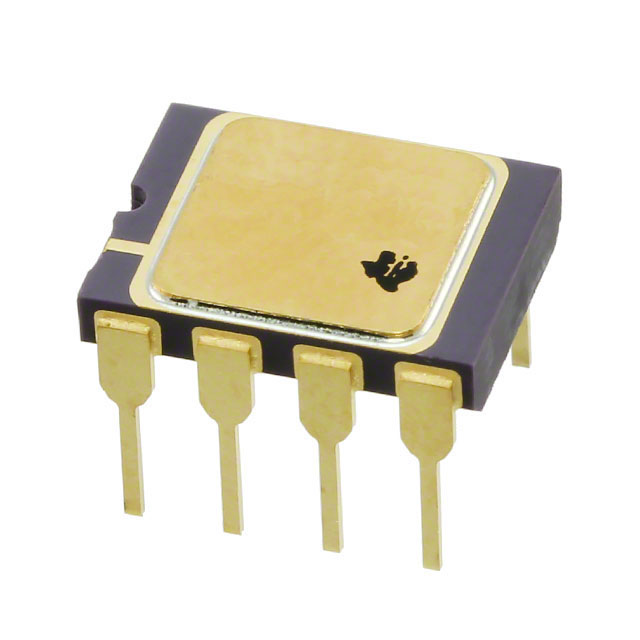
ORDERING INFORMATION (1)
ORDERABLE PART
NUMBER
TOP-SIDE MARKING
PACKAGE QTY | CARRIER
INA333SKGD1
NA
240 | TRAY
INA333SKGD2
NA
10 | TRAY
JD
INA333SJD
INA333SJD
1 | TUBE
HKJ
INA333SHKJ
INA333SHKJ
1 | TUBE
HKQ
INA333SHKQ
INA333SHKQ
1 | TUBE
PACKAGE (2)
TA
KGD
–55°C to 210°C
(1)
(2)
For the most current package and ordering information see the Package Option Addendum at the end of this document, or see the TI
web site at www.ti.com.
Package drawings, standard packaging quantities, thermal data, symbolization, and PCB design guidelines are available at
www.ti.com/packaging.
ABSOLUTE MAXIMUM RATINGS (1)
Supply voltage
Analog input voltage range
(2)
INA333
UNIT
+7
V
(V–) – 0.3 to (V+) + 0.3
Output short-circuit (3)
V
Continuous
Operating temperature range, TA
–55 to +210
°C
Storage temperature range, TSTG
–65 to +210
°C
+210
°C
Human body model (HBM)
4000
V
Charged device model (CDM)
1000
V
Machine model (MM)
200
V
Junction temperature, TJ
ESD rating
(1)
(2)
(3)
2
Stresses above these ratings may cause permanent damage. Exposure to absolute maximum conditions for extended periods may
degrade device reliability. These are stress ratings only, and functional operation of the device at these or any other conditions beyond
those specified is not implied.
Input terminals are diode-clamped to the power-supply rails. Input signals that can swing more than 0.3V beyond the supply rails should
be current limited to 10mA or less.
Short-circuit to ground.
Submit Documentation Feedback
Copyright © 2010–2013, Texas Instruments Incorporated
Product Folder Links: INA333-HT
�INA333-HT
www.ti.com
SBOS514C – MARCH 2010 – REVISED OCTOBER 2013
PIN CONFIGURATIONS
HKQ PACKAGE
(TOP VIEW)
JD OR HKJ PACKAGE
MSOP-8
(TOP VIEW)
RG
RG
8
1
8
1
RG
RG
V+
VINVIN+
VIN-
2
7
V+
VOUT
VIN+
3
6
VOUT
REF
V-
4
5
REF
5
4
V-
HKQ as formed or HKJ mounted dead bug
INA333
BARE DIE INFORMATION
DIE THICKNESS
BACKSIDE FINISH
BACKSIDE
POTENTIAL
BOND PAD
METALLIZATION COMPOSITION
15 mils.
Silicon with backgrind
V-
Al-Si-Cu (0.5%)
Origin
a
c
b
d
Submit Documentation Feedback
Copyright © 2010–2013, Texas Instruments Incorporated
Product Folder Links: INA333-HT
3
�INA333-HT
SBOS514C – MARCH 2010 – REVISED OCTOBER 2013
www.ti.com
Table 1. Bond Pad Coordinates in Microns
(1)
4
(1)
DESCRIPTION
PAD NUMBER
X MIN
Y MIN
X MAX
Y MAX
RG
1
250
1604.8
326
1680.8
VIN-
2
21.2
1300
97.2
1376
VIN+
3
21.2
978.5
97.2
1054.5
NC
4
21.2
748.65
97.2
824.65
V-
5
31.3
300
107.3
376
REF
6
1072.15
21.2
1148.15
97.2
VOUT
7
1299.8
216.2
1375.8
292.2
V+
8
1289.7
700
1365.7
776
RG
9
1071
1604.8
1147
1680.8
Substrate is N/C
Submit Documentation Feedback
Copyright © 2010–2013, Texas Instruments Incorporated
Product Folder Links: INA333-HT
�INA333-HT
www.ti.com
SBOS514C – MARCH 2010 – REVISED OCTOBER 2013
THERMAL CHARACTERISTICS FOR JD PACKAGE
over operating free-air temperature range (unless otherwise noted)
PARAMETER
TEST CONDITIONS
θJA
Junction-to-ambient thermal resistance (1)
θJB
Junction-to-board thermal resistance
θJC
Junction-to-case thermal resistance
(1)
(2)
High-K board
MIN
TYP
(2)
, no airflow
MAX
64.9
UNIT
°C/W
No airflow
83.4
High-K board without underfill
27.9
°C/W
6.49
°C/W
The intent of θJA specification is solely for a thermal performance comparison of one package to another in a standardized environment.
This methodolgy is not meant to and will not predict the performance of a package in an application-specific environment.
JED51-7, high effective thermal conductivity test board for leaded surface mount packages.
THERMAL CHARACTERISTICS FOR HKJ OR HKQ PACKAGE
over operating free-air temperature range (unless otherwise noted)
PARAMETER
θJC
Junction-to-case thermal resistance
MIN
TYP
MAX
to ceramic side of case
UNIT
5.7
to top of case lid (metal side of case)
°C/W
13.7
ELECTRICAL CHARACTERISTICS: VS = +1.8 V to +5.5 V
At TA = +25°C, RL = 10kΩ, VREF = VS/2, and G = 1, unless otherwise noted.
TA = –55°C to +125°C
PARAMETER
TEST CONDITIONS
MIN
TA = +210°C
TYP
MAX
MIN
±10 ±25/G
±25 ±75/G
TYP
MAX
UNIT
INPUT (1)
Offset voltage,
RTI (2)
VOSI
vs Temperature
vs Power supply
±0.1 ±0.5/G
PSR
1.8 V ≤ VS ≤ 5.5 V
±1 ±5/G
Long-term stability
See note
Turn-on time to specified
VOSI
μV
±15
(3)
0.2
(4) (5)
μV/°C
2.5 (4)
±5 ±15/G
μV/V
(6)
See Typical characteristics
See Typical characteristics
Impedance
Differential
ZIN
100 || 3
100 || 3
GΩ || pF
Common-mode
ZIN
100 || 3
100 || 3
GΩ || pF
Common-mode
voltage range
VCM
Common-mode
rejection
CMR
VO = 0 V
(V–) + 0.1
(V+) – 0.1
(V–) + 0.1
(V+) – 0.1 V
V
DC to 60 Hz
G=1
VCM = (V–) + 0.1 V to
(V+) – 0.1 V
80
90
dB
G = 10
VCM = (V–) + 0.1 V to
(V+) – 0.1 V
100
110
dB
G = 100
VCM = (V–) + 0.1 V to
(V+) – 0.1 V
100
115
110
dB
G = 1000
VCM = (V–) + 0.1 V to
(V+) – 0.1 V
100
115
113
dB
INPUT BIAS CURRENT
Input bias current
IB
vs Temperature
Input offset current
IOS
vs Temperature
(1)
(2)
(3)
(4)
(5)
(6)
±70
±200
See Typical Characteristic curve
±50
±1260
±2044
pA/°C
See Typical Characteristic curve
pA/°C
±200
See Typical Characteristic curve
pA
See Typical Characteristic curve
pA
Total VOS, Referred-to-input = (VOSI) + (VOSO/G).
RTI = Referred-to-input.
Temperature drift is measured from –55°C to +125°C.
G = 1000
Temperature drift is measured from 125°C to +210°C.
300-hour life test at +150°C demonstrated randomly distributed variation of approximately 1 μV.
Submit Documentation Feedback
Copyright © 2010–2013, Texas Instruments Incorporated
Product Folder Links: INA333-HT
5
�INA333-HT
SBOS514C – MARCH 2010 – REVISED OCTOBER 2013
www.ti.com
ELECTRICAL CHARACTERISTICS: VS = +1.8 V to +5.5 V (continued)
At TA = +25°C, RL = 10kΩ, VREF = VS/2, and G = 1, unless otherwise noted.
TA = –55°C to +125°C
PARAMETER
TEST CONDITIONS
MIN
TYP
TA = +210°C
MAX
MIN
TYP
MAX
UNIT
INPUT VOLTAGE NOISE
Input voltage noise
eNI
G = 100, RS = 0 Ω
f = 10 Hz
42
63
nV/√Hz
f = 100 Hz
40
70
nV/√Hz
f = 1 kHz
50
55
nV/√Hz
f = 0.1Hz to 10 Hz
2
6
μVPP
Input current noise
iN
f = 10Hz
f = 0.1Hz to 10Hz
100
fA/√Hz
2
pAPP
GAIN
Gain equation
G
1 + (100kΩ/RG)
Range of gain (7)
1
1 + (100kΩ/RG)
1000
100
V/V
1000
V/V
VS = 5.5 V,
(V–) + 100mV ≤ VO ≤
(V+) – 100mV
Gain error
G=1
±0.02
±0.1
G = 10
±0.05
±0.5
%
G = 100
±0.01
±0.5
±1.3
%
G = 1000
±0.43
±1.15
±1.7
%
%
GAIN (continued)
Gain vs Temperature
G=1
±1
±5
ppm/°C
G > 1 (8)
±15
±50
ppm/°C
Gain nonlinearity
VS = 5.5 V,
(V–) + 100mV ≤ VO ≤
(V+) – 100mV
G = 1 to 1000
RL = 10 kΩ
10
10
ppm
OUTPUT
Output voltage swing from
rail (9)
VS = 5.5 V, RL = 10 kΩ
Capacitive load drive
Short-circuit
current
ISC
Continuous to common
See note
(9)
50
185
mV
500
500
pF
–55, +5
–36, +1
mA
FREQUENCY
RESPONSE
Bandwidth, –3dB
Range of gain (7)
G=1
150
G = 10
35
G = 100
3.5
3.1
kHz
G = 1000
350
300
Hz
G=1
0.16
0.25
V/μs
G = 100
0.06
0.04
V/μs
Slew rate
Settling time to
0.01%
kHz
VS = 5 V, VO = 4 V Step
tS
G=1
VSTEP = 4 V
35
32
μs
G = 100
VSTEP = 4 V
240
326
μs
Settling time to
0.001%
(7)
(8)
(9)
6
SR
kHz
tS
Not recommend gain < 100 for 210°C application.
Does not include effects of external resistor RG.
See Typical Characteristics curve, Output Voltage Swing vs Output Current (Figure 31).
Submit Documentation Feedback
Copyright © 2010–2013, Texas Instruments Incorporated
Product Folder Links: INA333-HT
�INA333-HT
www.ti.com
SBOS514C – MARCH 2010 – REVISED OCTOBER 2013
ELECTRICAL CHARACTERISTICS: VS = +1.8 V to +5.5 V (continued)
At TA = +25°C, RL = 10kΩ, VREF = VS/2, and G = 1, unless otherwise noted.
TA = –55°C to +125°C
PARAMETER
TEST CONDITIONS
MIN
TYP
TA = +210°C
MAX
MIN
TYP
MAX
UNIT
G=1
VSTEP = 4 V
60
55
μs
G = 100
VSTEP = 4 V
500
530
μs
50% overdrive
52
28
μs
Overload recovery
REFERENCE INPUT
RIN
300
Voltage range
300
kΩ
V–
V+
V–
V+
V
+1.8
+5.5
+1.8
+5.5
V
±2.75
±0.9
±2.75
POWER SUPPLY
Voltage range
Single
Dual
±0.9
Quiescent current
IQ
VIN = VS/2
50
vs Temperature
V
μA
75
80
198
345
μA
TEMPERATURE RANGE
Specified temperature
range
–55
+125
–55
+210
°C
Operating temperature
range
–55
+125
–55
+210
°C
1000000
Estimated Life (Hours)
100000
10000
1000
Electromigration Fail Mode
100
10
1
110
130
150
170
190
210
230
Continous TJ (°C)
Notes
1. See datasheet for absolute maximum and minimum recommended operating conditions.
2. Silicon operating life design goal is 10 years at 105°C junction temperature (does not include package
interconnect life).
Figure 1. INA333SKGD1 Operating Life Derating Chart
Submit Documentation Feedback
Copyright © 2010–2013, Texas Instruments Incorporated
Product Folder Links: INA333-HT
7
�INA333-HT
SBOS514C – MARCH 2010 – REVISED OCTOBER 2013
www.ti.com
TYPICAL CHARACTERISTICS
At TA = +25°C, VS = 5V, RL = 10kΩ, VREF = midsupply, and G = 1, unless otherwise noted.
INPUT VOLTAGE OFFSET DRIFT
(–40°C to +125°C)
INPUT OFFSET VOLTAGE
VS = 5.5V
-25.0
-22.5
-20.0
-17.5
-15.0
-12.5
-10.0
-7.5
-5.0
-2.5
0
2.5
5.0
7.5
10.0
12.5
15.0
17.5
20.0
22.5
25.0
-0.10
-0.09
-0.08
-0.07
-0.06
-0.05
-0.04
-0.03
-0.02
-0.01
0
0.01
0.02
0.03
0.04
0.05
0.06
0.07
0.08
0.09
0.10
Population
Population
VS = 5.5V
Input Offset Voltage (mV)
Input Voltage Offset Drift (mV/°C)
Figure 2.
Figure 3.
INPUT VOLTAGE OFFSET DRIFT
(125°C to +210°C)
OUTPUT OFFSET VOLTAGE
VS = 5.5V
-75.0
-67.5
-60.0
-52.5
-45.0
-37.5
-30.0
-22.5
-15.0
-7.5
0
7.5
15.0
22.5
30.0
37.5
45.0
52.5
60.0
67.5
75.0
0.75
0.80
0.65
0.70
0.55
0.60
0.45
0.50
0.35
0.40
0.25
0.30
0.15
0.20
0.05
0.10
0.00
Population
Population
Vs = 5.5V
Gain = 1000
Output Offset Voltage (mV)
Input Voltage Offset Drift (µV/°C)
Figure 4.
Figure 5.
OUTPUT VOLTAGE OFFSET DRIFT
(–40°C to +125°C)
OFFSET VOLTAGE vs COMMON-MODE VOLTAGE
0
VS = 5.5V
VS = 1.8V
-5
VOS (mV)
Population
VS = 5V
-10
-15
-0.50
-0.45
-0.40
-0.35
-0.30
-0.25
-0.20
-0.15
-0.10
-0.05
0
0.05
0.10
0.15
0.20
0.25
0.30
0.35
0.40
0.45
0.50
-20
-25
0
0.5
1.0
1.5
2.0
2.5
3.0
3.5
4.0
4.5
5.0
VCM (V)
Output Voltage Offset Drift (mV/°C)
Figure 6.
8
Figure 7.
Submit Documentation Feedback
Copyright © 2010–2013, Texas Instruments Incorporated
Product Folder Links: INA333-HT
�INA333-HT
www.ti.com
SBOS514C – MARCH 2010 – REVISED OCTOBER 2013
TYPICAL CHARACTERISTICS (continued)
At TA = +25°C, VS = 5V, RL = 10kΩ, VREF = midsupply, and G = 1, unless otherwise noted.
0.1Hz TO 10Hz NOISE
0.1Hz TO 10Hz NOISE
Gain = 100
Noise (1mV/div)
Noise (0.5mV/div)
Gain = 1
Time (1s/div)
Time (1s/div)
Figure 8.
Figure 9.
SPECTRAL NOISE DENSITY
NONLINEARITY ERROR
0.012
Output Noise
100
100
Current Noise
Input Noise
10
10
2
(Input Noise) +
Total Input-Referred Noise =
(Output Noise)
2
G
1
1
0.1
1
10
100
1k
10k
DC Output Nonlinearity Error (%FSR)
1000
Current Noise Density (fA/ÖHz)
Voltage Noise Density (nV/ÖHz)
1000
G = 1000
G = 100
G = 10
G=1
0.008
VS = ±2.75V
0.004
0
-0.004
-0.008
-0.012
0
Frequency (Hz)
0.5
1.0
1.5
2.0
2.5
3.0 3.5
4.0
4.5
5.0
5.5
VOUT (V)
Figure 10.
Figure 11.
LARGE SIGNAL RESPONSE
LARGE-SIGNAL STEP RESPONSE
Output Voltage (1V/div)
Gain = 100
Output Voltage (1V/div)
Gain = 1
Time (25ms/div)
Time (100ms/div)
Figure 12.
Figure 13.
Submit Documentation Feedback
Copyright © 2010–2013, Texas Instruments Incorporated
Product Folder Links: INA333-HT
9
�INA333-HT
SBOS514C – MARCH 2010 – REVISED OCTOBER 2013
www.ti.com
TYPICAL CHARACTERISTICS (continued)
At TA = +25°C, VS = 5V, RL = 10kΩ, VREF = midsupply, and G = 1, unless otherwise noted.
SMALL-SIGNAL STEP RESPONSE
SMALL-SIGNAL STEP RESPONSE
Output Voltage (50mV/div)
Gain = 100
Output Voltage (50mV/div)
Gain = 1
Time (10ms/div)
Time (100ms/div)
Figure 14.
Figure 15.
SETTLING TIME vs GAIN
STARTUP SETTLING TIME
10000
Gain = 1
Supply
Supply (1V/div)
Time (ms)
VOUT
0.001%
100
0.01%
0.1%
10
1
VOUT (50mV/div)
1000
Time (50ms/div)
1000
100
10
Gain (V/V)
Figure 16.
Figure 17.
GAIN vs FREQUENCY
COMMON-MODE REJECTION RATIO
80
VS = 5.5V
G = 1000
60
G = 100
G = 10
Population
Gain (dB)
40
20
G=1
0
-20
-60
10
100
1k
10k
Frequency (Hz)
100k
1M
-100
-90
-80
-70
-60
-50
-40
-30
-20
-10
0
10
20
30
40
50
60
70
80
90
100
-40
CMRR (mV/V)
Figure 18.
10
Figure 19.
Submit Documentation Feedback
Copyright © 2010–2013, Texas Instruments Incorporated
Product Folder Links: INA333-HT
�INA333-HT
www.ti.com
SBOS514C – MARCH 2010 – REVISED OCTOBER 2013
TYPICAL CHARACTERISTICS (continued)
At TA = +25°C, VS = 5V, RL = 10kΩ, VREF = midsupply, and G = 1, unless otherwise noted.
COMMON-MODE REJECTION RATIO vs FREQUENCY
160
140
G = 1000
120
4
2
0
-2
-4
-6
-8
-10
G = 100
CMRR (dB)
CMRR (µV/V)
COMMON-MODE REJECTION RATIO vs TEMPERATURE
10
Vs = ±2.75V
8
Vs = ±0.9V
6
G = 1000
G = 100
100
80
60
G=1
40
G = 10
20
-65 -40 -15 10
0
35 60 85 110 135 160 185 210
10
Frequency (Hz)
Figure 20.
Figure 21.
TYPICAL COMMON-MODE RANGE vs OUTPUT VOLTAGE
TYPICAL COMMON-MODE RANGE vs OUTPUT VOLTAGE
2.0
5
VS = ±2.5V
VREF = 0
Common-Mode Voltage (V)
2.5
Common-Mode Voltage (V)
100k
10k
1k
100
Temperature (°C)
1.0
All Gains
0
-1.0
VS = +5V
VREF = 0
4
3
All Gains
2
1
-2.0
2.5
-2.5 -2.0
0
0
-1.0
2.0
1.0
0
2.5
5
4
Output Voltage (V)
Figure 22.
Figure 23.
TYPICAL COMMON-MODE RANGE vs OUTPUT VOLTAGE
TYPICAL COMMON-MODE RANGE vs OUTPUT VOLTAGE
0.7
1.8
VS = ±0.9V
VREF = 0
0.5
0.3
0.1
All Gains
-0.1
-0.3
-0.5
-0.7
-0.9
-0.9
VS = +1.8V
VREF = 0
1.6
Common-Mode Voltage (V)
0.9
Common-Mode Voltage (V)
3
2
1
Output Voltage (V)
1.4
1.2
1.0
All Gains
0.8
0.6
0.4
0.2
0
-0.7
-0.5
-0.3
-0.1
0.1
0.3
0.5
0.7
0.9
0
Output Voltage (V)
0.2
0.4
0.5
0.8
1.0
1.2
1.4
1.6
1.8
Output Voltage (V)
Figure 24.
Figure 25.
Submit Documentation Feedback
Copyright © 2010–2013, Texas Instruments Incorporated
Product Folder Links: INA333-HT
11
�INA333-HT
SBOS514C – MARCH 2010 – REVISED OCTOBER 2013
www.ti.com
TYPICAL CHARACTERISTICS (continued)
At TA = +25°C, VS = 5V, RL = 10kΩ, VREF = midsupply, and G = 1, unless otherwise noted.
POSITIVE POWER-SUPPLY REJECTION RATIO
NEGATIVE POWER-SUPPLY REJECTION RATIO
160
160
140
140
G = 1000
-PSRR (dB)
+PSRR (dB)
100
G = 100
80
60
G = 10
20
80
G = 10
60
40
G=1
0
0
1
10
100
1k
10k
100k
-20
1M
0.1
10
1
100
1k
Frequency (Hz)
Frequency (Hz)
Figure 26.
Figure 27.
INPUT BIAS CURRENT vs TEMPERATURE
10k
100k
1M
| INPUT BIAS CURRENT | vs COMMON-MODE VOLTAGE
200
+IB
-IB
180
160
140
| IB | (pA)
IB (pA)
G = 1000
100
20
G=1
1400
1200
1000
800
600
400
200
0
-200
G = 100
120
120
40
VS = 5V
Vs = ±0.9V
120
100
80
60
Vs = ±2.75V
VS = 5V
40
20
VS = 1.8V
0
0
-65 -40 -15 10 35 60 85 110 135 160 185 210
0.5
1.0
1.5
2.0
2.5
3.0
3.5
4.0
4.5
5.0
VCM (V)
Temperature (°C)
Figure 28.
Figure 29.
INPUT OFFSET CURRENT vs TEMPERATURE
OUTPUT VOLTAGE SWING vs OUTPUT CURRENT
150
50
VOUT (V)
IOS (pA)
100
Vs = ±2.75V
0
Vs = ±0.9V
-50
-65 -40 -15 10 35 60 85 110 135 160 185 210
(V+)
(V+) - 0.25
(V+) - 0.50
(V+) - 0.75
(V+) - 1.00
(V+) - 1.25
(V+) - 1.50
(V+) - 1.75
VS = ±2.75V
VS = ±0.9V
(V-) + 1.75
(V-) + 1.50
(V-) + 1.25
(V-) + 1.00
(V-) + 0.75
(V-) + 0.50
(V-) + 0.25
(V-)
+125°C
+25°C
-40°C
0
10
20
30
40
50
60
IOUT (mA)
Temperature (°C)
Figure 30.
12
Figure 31.
Submit Documentation Feedback
Copyright © 2010–2013, Texas Instruments Incorporated
Product Folder Links: INA333-HT
�INA333-HT
www.ti.com
SBOS514C – MARCH 2010 – REVISED OCTOBER 2013
TYPICAL CHARACTERISTICS (continued)
At TA = +25°C, VS = 5V, RL = 10kΩ, VREF = midsupply, and G = 1, unless otherwise noted.
QUIESCENT CURRENT vs TEMPERATURE
QUIESCENT CURRENT vs COMMON-MODE VOLTAGE
80
250
70
VS = 5V
200
60
Vs = 5V
IQ (mA)
IQ (uA)
50
150
40
VS = 1.8V
30
100
20
50
10
Vs = 1.8V
0
0
0
-65 -40 -15 10 35 60 85 110 135 160 185 210
1.0
3.0
2.0
4.0
5.0
VCM (V)
Temperature (°C)
Figure 32.
Figure 33.
Submit Documentation Feedback
Copyright © 2010–2013, Texas Instruments Incorporated
Product Folder Links: INA333-HT
13
�INA333-HT
SBOS514C – MARCH 2010 – REVISED OCTOBER 2013
www.ti.com
APPLICATION INFORMATION
Application information below is provided for
commercial temperature as a reference and not for
high temperature.
It is not recommended to use a gain < 100 for high
temperature (210°C) applications. For gains > 100 in
such applications, a compensation circuit is needed
at pins 1 and 8. The circuit is needed at each pin and
consists of a resistor in series with a capacitor
referenced to ground. Recommended values for the
resistor and capacitor are 3.5 kΩ and 10 nF
respectively.
Figure 34 shows the basic connections required for
operation of the INA333. Good layout practice
mandates the use of bypass capacitors placed close
to the device pins as shown.
The output of the INA333 is referred to the output
reference (REF) terminal, which is normally
grounded. This connection must be low-impedance to
assure good common-mode rejection. Although 15 Ω
or less of stray resistance can be tolerated while
maintaining specified CMRR, small stray resistances
of tens of ohms in series with the REF pin can cause
noticeable degradation in CMRR.
14
SETTING THE GAIN
Gain of the INA333 is set by a single external
resistor, RG, connected between pins 1 and 8. The
value of RG is selected according to Equation 1:
G = 1 + (100 kΩ/RG)
(1)
(1)
Table 2 lists several commonly-used gains and
resistor values. The 100 kΩ term in Equation 1
comes from the sum of the two internal feedback
resistors of A1 and A2. These on-chip resistors are
laser trimmed to accurate absolute values. The
accuracy and temperature coefficient of these
resistors are included in the gain accuracy and drift
specifications of the INA333.
The stability and temperature drift of the external gain
setting resistor, RG, also affects gain. The contribution
of RG to gain accuracy and drift can be directly
inferred from the gain Equation 1. Low resistor values
required for high gain can make wiring resistance
important. Sockets add to the wiring resistance and
contribute additional gain error (possibly an unstable
gain error) in gains of approximately 100 or greater.
To ensure stability, avoid parasitic capacitance of
more than a few picofarads at the RG connections.
Careful matching of any parasitics on both RG pins
maintains optimal CMRR over frequency.
Submit Documentation Feedback
Copyright © 2010–2013, Texas Instruments Incorporated
Product Folder Links: INA333-HT
�INA333-HT
www.ti.com
SBOS514C – MARCH 2010 – REVISED OCTOBER 2013
V+
0.1mF
7
VIN-
2
RFI Filter
150kW
150kW
A1
VO = G ´ (VIN+ - VIN-)
RFI Filter
1
50kW
RG
G=1+
6
A3
50kW
+
8
Load VO
RFI Filter
VIN+
100kW
RG
150kW
150kW
A2
3
-
5
Ref
RFI Filter
INA333
4
0.1mF
V-
Also drawn in simplified form:
VINRG
VO
INA333
Ref
VIN+
Figure 34. Basic Connections
Table 2. Commonly-Used Gains and Resistor Values
DESIRED GAIN
(1)
RG (Ω)
(1)
NEAREST 1% RG (Ω)
1
NC
2
100k
100k
NC
5
25k
24.9k
10
11.1k
11k
20
5.26k
5.23k
50
2.04k
2.05
100
1.01k
1k
200
502.5
499
500
200.4
200
1000
100.1
100
NC denotes no connection. When using the SPICE model, the simulation will not converge unless a resistor is connected to the RG pins;
use a very large resistor value.
Submit Documentation Feedback
Copyright © 2010–2013, Texas Instruments Incorporated
Product Folder Links: INA333-HT
15
�INA333-HT
SBOS514C – MARCH 2010 – REVISED OCTOBER 2013
www.ti.com
INTERNAL OFFSET CORRECTION
The INA333 internal op amps use an auto-calibration
technique with a time-continuous 350-kHz op amp in
the signal path. The amplifier is zero-corrected every
8 μs using a proprietary technique. Upon power-up,
the amplifier requires approximately 100 μs to
achieve specified VOS accuracy. This design has no
aliasing or flicker noise.
OFFSET TRIMMING
Most applications require no external offset
adjustment; however, if necessary, adjustments can
be made by applying a voltage to the REF terminal.
Figure 35 shows an optional circuit for trimming the
output offset voltage. The voltage applied to REF
terminal is summed at the output. The op amp buffer
provides low impedance at the REF terminal to
preserve good common-mode rejection.
Input circuitry must provide a path for this input bias
current for proper operation. Figure 36 illustrates
various provisions for an input bias current path.
Without a bias current path, the inputs will float to a
potential that exceeds the common-mode range of
the INA333, and the input amplifiers will saturate. If
the differential source resistance is low, the bias
current return path can be connected to one input
(see the thermocouple example in Figure 36). With
higher source impedance, using two equal resistors
provides a balanced input with possible advantages
of lower input offset voltage as a result of bias current
and better high-frequency common-mode rejection.
Microphone,
Hydrophone,
etc.
INA333
47kW
VIN-
V+
RG
VIN+
47kW
INA333
VO
100mA
1/2 REF200
Ref
Thermocouple
OPA333
±10mV
Adjustment Range
INA333
100W
10kW
10kW
100W
100mA
1/2 REF200
INA333
V-
(1) REF200 and OPA333 are not tested or characterized at 210°C.
Center tap provides
bias current return.
Figure 35. Optional Trimming of Output Offset
Voltage
Figure 36. Providing an Input Common-Mode
Current Path
NOISE PERFORMANCE
The auto-calibration technique used by the INA333
results in reduced low frequency noise, typically only
50 nV/√Hz, (G = 100). The spectral noise density can
be seen in detail in Figure 10. Low frequency noise of
the INA333 is approximately 1 μVPP measured from
0.1 Hz to 10 Hz, (G = 100).
INPUT BIAS CURRENT RETURN PATH
The input impedance of the INA333 is extremely
high—approximately 100 GΩ. However, a path must
be provided for the input bias current of both inputs.
This input bias current is typically ±70 pA. High input
impedance means that this input bias current
changes very little with varying input voltage.
16
INPUT COMMON-MODE RANGE
The linear input voltage range of the input circuitry of
the INA333 is from approximately 0.1 V below the
positive supply voltage to 0.1 V above the negative
supply. As a differential input voltage causes the
output voltage to increase, however, the linear input
range is limited by the output voltage swing of
amplifiers A1 and A2. Thus, the linear common-mode
input range is related to the output voltage of the
complete amplifier. This behavior also depends on
supply voltage—see Typical Characteristic curves
Typical Common-Mode Range vs Output Voltage
(Figure 22 to Figure 25).
Submit Documentation Feedback
Copyright © 2010–2013, Texas Instruments Incorporated
Product Folder Links: INA333-HT
�INA333-HT
www.ti.com
SBOS514C – MARCH 2010 – REVISED OCTOBER 2013
Input overload conditions can produce an output
voltage that appears normal. For example, if an input
overload condition drives both input amplifiers to the
respective positive output swing limit, the difference
voltage measured by the output amplifier is near
zero. The output of the INA333 is near 0 V even
though both inputs are overloaded.
+3V
3V
2V - DV
RG
300W
VO
INA333
Ref
2V + DV
OPERATING VOLTAGE
150W
The INA333 operates over a power-supply range of
+1.8 V to +5.5 V (±0.9 V to ±2.75 V). Supply voltages
higher than +7 V (absolute maximum) can
permanently damage the device. Parameters that
vary over supply voltage or temperature are shown in
the Typical Characteristics section of this data sheet.
R1
1.5V
(1)
(1) R1 creates proper common-mode voltage, only for low-voltage
operation—see the Single-Supply Operation section.
Figure 37. Single-Supply Bridge Amplifier
LOW VOLTAGE OPERATION
INPUT PROTECTION
The INA333 can be operated on power supplies as
low as ±0.9 V. Most parameters vary only slightly
throughout this supply voltage range—see the Typical
Characteristics section. Operation at very low supply
voltage requires careful attention to assure that the
input voltages remain within the linear range. Voltage
swing requirements of internal nodes limit the input
common-mode range with low power-supply voltage.
The Typical Characteristic curves Typical CommonMode Range vs Output Voltage (Figure 22 to
Figure 25) show the range of linear operation for
various supply voltages and gains.
The input terminals of the INA333 are protected with
internal diodes connected to the power-supply rails.
These diodes clamp the applied signal to prevent it
from damaging the input circuitry. If the input signal
voltage can exceed the power supplies by more than
0.3 V, the input signal current should be limited to
less than 10 mA to protect the internal clamp diodes.
This current limiting can generally be done with a
series input resistor. Some signal sources are
inherently current-limited and do not require limiting
resistors.
GENERAL LAYOUT GUIDELINES
SINGLE-SUPPLY OPERATION
The INA333 can be used on single power supplies of
+1.8 V to +5.5 V. Figure 37 illustrates a basic singlesupply circuit. The output REF terminal is connected
to mid-supply. Zero differential input voltage demands
an output voltage of mid-supply. Actual output voltage
swing is limited to approximately 50 mV above
ground, when the load is referred to ground as
shown. The typical characteristic curve Output
Voltage Swing vs Output Current (Figure 31) shows
how the output voltage swing varies with output
current.
With single-supply operation, VIN+ and VIN– must both
be 0.1V above ground for linear operation. For
instance, the inverting input cannot be connected to
ground to measure a voltage connected to the
noninverting input.
To illustrate the issues affecting low voltage
operation, consider the circuit in Figure 37. It shows
the INA333 operating from a single 3-V supply. A
resistor in series with the low side of the bridge
assures that the bridge output voltage is within the
common-mode range of the amplifier inputs.
Attention to good layout practices is always
recommended. Keep traces short and, when
possible, use a printed circuit board (PCB) ground
plane with surface-mount components placed as
close to the device pins as possible. Place a 0.1-μF
bypass capacitor closely across the supply pins.
These guidelines should be applied throughout the
analog circuit to improve performance and provide
benefits such as reducing the electromagneticinterference (EMI) susceptibility.
Instrumentation amplifiers vary in the susceptibility to
radio-frequency interference (RFI). RFI can generally
be identified as a variation in offset voltage or dc
signal levels with changes in the interfering RF signal.
The INA333 has been specifically designed to
minimize susceptibility to RFI by incorporating
passive RC filters with an 8-MHz corner frequency at
the VIN+ and VIN– inputs. As a result, the INA333
demonstrates remarkably low sensitivity compared to
previous generation devices. Strong RF fields may
continue to cause varying offset levels, however, and
may require additional shielding.
APPLICATION IDEAS
Additional application ideas are shown in Figure 38 to
Figure 41.
Submit Documentation Feedback
Copyright © 2010–2013, Texas Instruments Incorporated
Product Folder Links: INA333-HT
17
�INA333-HT
SBOS514C – MARCH 2010 – REVISED OCTOBER 2013
www.ti.com
2.8kW
LA
RA
RG/2
INA333
VO
Ref
2.8kW
G = 10
390kW
1/2
OPA2333
RL
1/2
OPA2333
10kW
390kW
Figure 38. ECG Amplifier With Right-Leg Drive
+VS
R1
100kW
fLPF = 150Hz
C4
1.06nF
1/2
OPA2333
RA
+VS
R2
100kW
+VS
2
R6
100kW
1/2
OPA2333
7
1
RG
R8
100kW
+VS
3
dc
R3
100kW
GINA = 5
6
INA333
8
LL
4
5
ac
1/2
OPA2333
C3
1mF
R12
5kW
+VS
OPA333
R13
318kW
VOUT
GOPA = 200
+VS
1/2
OPA2333
Wilson
LA
R14
1MW
GTOT = 1kV/V
R7
100kW
VCENTRAL
C1
47pF
(RA + LA + LL)/3
fHPF = 0.5Hz
(provides ac signal coupling)
1/2 VS
R5
390kW
+VS
R4
100kW
R9
20kW
1/2
OPA2333
RL
Inverted
VCM
+VS
VS = +2.7V to +5.5V
1/2
OPA2333
BW = 0.5Hz to 150Hz
+VS
R10
1MW
1/2 VS
C2
0.64mF
R11
1MW
fO = 0.5Hz
(1) OPA333 is not tested or characterized at 210°C.
Figure 39. Single-Supply, Very Low Power, ECG Circuit
18
Submit Documentation Feedback
Copyright © 2010–2013, Texas Instruments Incorporated
Product Folder Links: INA333-HT
�INA333-HT
www.ti.com
SBOS514C – MARCH 2010 – REVISED OCTOBER 2013
TINA-TI
(FREE DOWNLOAD SOFTWARE)
Virtual instruments offer users the ability to select
input waveforms and probe circuit nodes, voltages,
and waveforms, creating a dynamic quick-start tool.
Using TINA-TI SPICE-Based Analog Simulation
Program with the INA333
Figure 40 and Figure 41 show example TINA-TI
circuits for the INA333 that can be used to develop,
modify, and assess the circuit design for specific
applications. Links to download these simulation files
are given below.
TINA is a simple, powerful, and easy-to-use circuit
simulation program based on a SPICE engine. TINATI is a free, fully functional version of the TINA
software, preloaded with a library of macromodels in
addition to a range of both passive and active
models. It provides all the conventional dc, transient,
and frequency domain analysis of SPICE as well as
additional design capabilities.
NOTE: these files require that either the TINA
software (from DesignSoft) or TINA-TI software be
installed. Download the free TINA-TI software from
the TINA-TI folder.
Available as a free download from the Analog eLab
Design Center, TINA-TI offers extensive postprocessing capability that allows users to format
results in a variety of ways.
VoA1
1/2 of matched
monolithic dual
NPN transistors
(example: MMDT3904)
RELATED PRODUCTS
For monolithic logarithmic amplifiers (such as LOG112 or LOG114) see the link in footnote 1.
Vout
VM1
8
Ref
6
RG V+
U5 OPA369
+
5
+
7
VCC
VCC
3
Vdiff
Vref+
1/2 of matched
monolithic dual
NPN transistors
(example: MMDT3904)
-
R8 10k
Out
+
U1 OPA335
VCC
4
5
1
U1 INA333
Optional buffer for driving
SAR converters with
sampling systems of ³ 33kHz.
VCC
V
4
RG V-
C1 1n
+
Vref+
Vref+
Input I 10n
+
+
_
Vref+
2
1
R3 14k
2
3
VoA2
3
Vref+
uC Vref/2 2.5
1
+
uC Vref/2 2.5
2
+
4
5
V1 5
NOTE: Temperature compensation
of logging transistors is not shown.
U6 OPA369
VCC
Rset 2.5M
(1) The following link launches the TI logarithmic amplifiers web page: Logarithmic Amplifier Products Home Page
(2) OPA369 and OPA335 are not characterized at 210°C.
Figure 40. Low-Power Log Function Circuit for Portable Battery-Powered Systems
(Example Glucose Meter)
To download a compressed file that contains the TINA-TI simulation file for this circuit, click the following link:
Log Circuit.
Submit Documentation Feedback
Copyright © 2010–2013, Texas Instruments Incorporated
Product Folder Links: INA333-HT
19
�INA333-HT
SBOS514C – MARCH 2010 – REVISED OCTOBER 2013
www.ti.com
3V
R1
2kW
RWa
3W
EMU21 RTD3
-
Pt100 RTD
VT+
U2
OPA333
RWb
3W
+
RTD+
VT 25
+
2 _
3V
VT-
RTD-
Mon+
RGAIN
100kW
Mon-
+
U1 INA333
VDIFF
Out
Ref
8
RG V+
RWc
4W
Temp (°C)
(Volts = °C)
1
4
RG V-
RZERO
100W
3
PGA112
MSP430
6
5
+
7
V
VREF+
3V
VRTD
RWd
3W
RTD Resistance
(Volts = Ohms)
+
+
A
IREF1
A
IREF2
3V
U1 REF3212
VREF
3V
VREF
VREF
Use BF861A
EN
OUTF
+
In
OUTS
GNDF GNDS
C7
470nF
S
+
T3 BF256A
OPA3331 OPA333
Use BF861A
3V
T1 BF256A
+
+
U3
OPA333
3V
-
G
-
V4 3
RSET1
2.5kW
RSET2
2.5kW
(1) RWa, RWb, RWc, and RWd simulate wire resistance. These resistors are included to show the four-wire sense technique immunity to
line mismatches. This method assumes the use of a four-wire RTD.
(2) In this diagram, only INA333 is tested and characterized at 210°C.
Figure 41. Four-Wire, 3V Conditioner for a PT100 RTD With Programmable Gain Acquisition System
To download a compressed file that contains the TINA-TI simulation file for this circuit, click the following link:
PT100 RTD.
20
Submit Documentation Feedback
Copyright © 2010–2013, Texas Instruments Incorporated
Product Folder Links: INA333-HT
�PACKAGE OPTION ADDENDUM
www.ti.com
15-Jun-2022
PACKAGING INFORMATION
Orderable Device
Status
(1)
Package Type Package Pins Package
Drawing
Qty
Eco Plan
(2)
Lead finish/
Ball material
MSL Peak Temp
Op Temp (°C)
Device Marking
(3)
Samples
(4/5)
(6)
INA333SHKJ
ACTIVE
CFP
HKJ
8
25
RoHS & Green
Call TI
N / A for Pkg Type
-55 to 210
INA333S
HKJ
Samples
INA333SHKQ
ACTIVE
CFP
HKQ
8
25
RoHS & Green
AU
N / A for Pkg Type
-55 to 210
INA333S
HKQ
Samples
INA333SJD
ACTIVE
CDIP SB
JD
8
45
RoHS & Green
Call TI
N / A for Pkg Type
-55 to 210
INA333SJD
Samples
INA333SKGD1
ACTIVE
XCEPT
KGD
0
240
RoHS & Green
Call TI
N / A for Pkg Type
-55 to 210
Samples
INA333SKGD2
ACTIVE
XCEPT
KGD
0
10
RoHS & Green
Call TI
N / A for Pkg Type
-55 to 210
Samples
(1)
The marketing status values are defined as follows:
ACTIVE: Product device recommended for new designs.
LIFEBUY: TI has announced that the device will be discontinued, and a lifetime-buy period is in effect.
NRND: Not recommended for new designs. Device is in production to support existing customers, but TI does not recommend using this part in a new design.
PREVIEW: Device has been announced but is not in production. Samples may or may not be available.
OBSOLETE: TI has discontinued the production of the device.
(2)
RoHS: TI defines "RoHS" to mean semiconductor products that are compliant with the current EU RoHS requirements for all 10 RoHS substances, including the requirement that RoHS substance
do not exceed 0.1% by weight in homogeneous materials. Where designed to be soldered at high temperatures, "RoHS" products are suitable for use in specified lead-free processes. TI may
reference these types of products as "Pb-Free".
RoHS Exempt: TI defines "RoHS Exempt" to mean products that contain lead but are compliant with EU RoHS pursuant to a specific EU RoHS exemption.
Green: TI defines "Green" to mean the content of Chlorine (Cl) and Bromine (Br) based flame retardants meet JS709B low halogen requirements of