User's Guide
SBOU122B – September 2013 – Revised August 2016
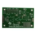
Universal Instrumentation Amplifier Evaluation Module
This user's guide describes the characteristics, operation, and use of two evaluation modules (EVMs) that
are compatible with a variety of instrumentation amplifiers (IAs). The schematics and bills of material
(BOM) are identical for both EVMs. The only difference is that one EVM is compatible with devices in
VSSOP-8 (DGK) packages, and the other EVM is compatible with devices in SOIC-8 (D) packages. They
are designed to evaluate the performance of the devices in both single- and dual-supply configurations.
This document includes the schematic, printed circuit board (PCB) layouts, and BOM. Throughout this
document the terms evaluation board, evaluation module, and EVM are synonymous with the Universal IA
EVM.
1
2
3
4
5
6
7
Contents
Overview ..................................................................................................................... 2
PCB Layout ................................................................................................................... 3
Schematic ..................................................................................................................... 5
EVM Components ........................................................................................................... 6
Quick Start .................................................................................................................... 7
Bill of Materials ............................................................................................................. 10
Related Documentation from Texas Instruments ...................................................................... 10
List of Figures
1
IA Pinout ...................................................................................................................... 2
2
Universal IA EVM Schematic Side (VSSOP-8) .......................................................................... 3
3
Universal IA EVM Component Side (VSSOP-8) ......................................................................... 3
4
Universal IA EVM Schematic Side (SOIC-8) ............................................................................. 4
5
Universal IA EVM Component Side (SOIC-8)
6
7
8
9
...........................................................................
Universal IA EVM Schematic...............................................................................................
Dual-Supply Configuration ..................................................................................................
Single-Supply Configuration, Direct REF Connection ..................................................................
Single-Supply Configuration, Buffered REF Connection ...............................................................
4
5
7
8
9
Trademarks
X2Y is a registered trademark of X2Y Attenuators LLC.
All other trademarks are the property of their respective owners.
SBOU122B – September 2013 – Revised August 2016
Submit Documentation Feedback
Universal Instrumentation Amplifier Evaluation Module
Copyright © 2013–2016, Texas Instruments Incorporated
1
�Overview
www.ti.com
1
Overview
1.1
Features
These EVMs are intended to provide basic functional evaluation of the amplifiers shown in Table 1 with
the pinout shown in Figure 1. The EVMs provide the following features:
•
•
•
•
•
1.2
Intuitive evaluation with the silkscreen schematic
Easy access to nodes with surface-mount test points
Advanced evaluation with two prototype areas
Reference voltage source flexibility
Convenient input and output filtering
IA Pinout
The EVMs are intended to evaluate IAs that have the pinout shown in Figure 1.
U1
IA
RG
1
8
RG
±IN
2
7
+VS
+IN
3
6
VOUT
±VS
4
5
REF
+
Figure 1. IA Pinout
1.3
Compatible Devices
Devices that are compatible with at least one of the EVMs are shown in Table 1.
Table 1. Compatible Devices
Device
VSSOP-8 (DGK) EVM
INA118
X
INA121
X
INA122
X
INA126
X
X
INA128
X
INA129
X
INA141
X
INA155
X
INA156
X
INA188
INA333
2
SOIC-8 (D) EVM
Universal Instrumentation Amplifier Evaluation Module
X
X
X
SBOU122B – September 2013 – Revised August 2016
Submit Documentation Feedback
Copyright © 2013–2016, Texas Instruments Incorporated
�PCB Layout
www.ti.com
2
PCB Layout
The schematic and component sides of the VSSOP-8 EVM are shown in Figure 2 and Figure 3,
respectively.
NOTE: Board layouts are not to scale. These figures are intended to show how the board is laid out;
they are not intended to be used for manufacturing PCBs.
Figure 2. Universal IA EVM Schematic Side (VSSOP-8)
Figure 3. Universal IA EVM Component Side (VSSOP-8)
SBOU122B – September 2013 – Revised August 2016
Submit Documentation Feedback
Universal Instrumentation Amplifier Evaluation Module
Copyright © 2013–2016, Texas Instruments Incorporated
3
�PCB Layout
www.ti.com
The schematic and component sides of the SOIC-8 EVM are shown in Figure 4 and Figure 5, respectively.
Figure 4. Universal IA EVM Schematic Side (SOIC-8)
Figure 5. Universal IA EVM Component Side (SOIC-8)
4
Universal Instrumentation Amplifier Evaluation Module
SBOU122B – September 2013 – Revised August 2016
Submit Documentation Feedback
Copyright © 2013–2016, Texas Instruments Incorporated
�Schematic
www.ti.com
3
Schematic
Figure 6 shows the schematic for the PCB.
RG
V+
U1
C10
V±IN
IA
R1
C1
RG
0
±IN
C2
V+IN
R2
SMA
0.1 PF
RG
VO
+VS
RO
+
SMA
C7
V±
0
+IN
VOUT
±VS
REF
REF
0
CO
SMA
C3
C9
R5
C6
GND
0.1 PF
R3
OAV+
C13
C12
C4
U2
1
OAVIN+ OAVIN±
8
R4
2
7
+
OAV±
C11
3
6
4
5
C5
Figure 6. Universal IA EVM Schematic
SBOU122B – September 2013 – Revised August 2016
Submit Documentation Feedback
Universal Instrumentation Amplifier Evaluation Module
Copyright © 2013–2016, Texas Instruments Incorporated
5
�EVM Components
www.ti.com
4
EVM Components
4.1
Power
Power is applied to the device with test points V+ and V–. For the unpopulated device (U2), power is
applied using test points OAV+ and OAV–.
4.2
Inputs
Inputs are applied to the device using test points V+IN and V–IN. Alternately, they can be applied by
populating the input SMA connectors (J1 and J2). The inputs for U2 are applied through test points
OAVIN+ and OAVIN–.
4.2.1
Input Filtering
R1, R2, and C1 through C3 provide the ability to apply common-mode and differential-mode filtering to the
inputs. The cutoff frequencies for the filters are shown in Equation 1 and Equation 2. For best
performance, make C2 approximately ten times larger than C1 and C3.. These calculations presume R1 =
R2 and C1 = C3.
Common-mode cutoff frequency:
fc-cm =
1
2S u R1 u C1
(1)
Differential-mode cutoff frequency:
fc-dm =
4.3
1
§
2S R1 R2 ¨ C2
©
C1 ·
2 ¸¹
(2)
Output
Access the output of the device with test point VO or by by populating the output SMA connector (J3).
4.3.1
Output Filtering
RO and CO provide the ability to apply a single-pole RC output filter. The cutoff frequency of the output
filter is calculated as shown in Equation 3:
1
fc-o =
2S u RO u CO
(3)
4.4
Reference
There are multiple methods of applying a reference voltage to the device. A straightforward approach is to
apply a voltage to the REF test point with U2 unpopulated. If a buffered voltage is desired, U2 can be
populated with an operational amplifier in an appropriate SOIC-8 package and pinout. If the reference
voltage is GND, either R5 can be populated with a 0-Ω resistor, or the REF test point can be connected to
GND.
4.5
Prototype Area
Two prototype areas are provided for flexible evaluation. They can be used, for example, to prototype a
voltage divider for a buffered reference voltage, or to supply a direct reference voltage with a device such
as the REF3225.
6
Universal Instrumentation Amplifier Evaluation Module
SBOU122B – September 2013 – Revised August 2016
Submit Documentation Feedback
Copyright © 2013–2016, Texas Instruments Incorporated
�EVM Components
www.ti.com
4.6
Miscellaneous
C6, C7, C9, and C10 are the supply bypass capacitors for the device. C9 and C10 are prepopulated with
0.1 µF capacitors that usually provide adequate power supply bypassing for U1. Refer to the
instrumentation amplifier data sheet for further information. Similarly, C4, C5, C11, and C12 can be
populated to provide supply bypassing for U2. Refer to the buffer amplifier data sheet for further
information. C8 can be used with an X2Y® capacitor.
5
Quick Start
The procedures presented in this section describe how to quickly set up and use the Universal IA EVM for
evaluation in dual-supply and single-supply configurations.
5.1
Dual-Supply Configuration
Figure 7 shows an example of how to set up the EVM for dual-supply operation.
V+
U1
C10
V±IN
IA
0.1 PF
R1
RG
0
C7
±IN
VO
+VS
RO
+
R2
V±
+VS
RG
Input Signal
V+IN
+
±
+IN
VOUT
±VS
REF
0
0
±VS
+
±
C9
R5
C6
0
0.1 PF
GND
Figure 7. Dual-Supply Configuration
The following connections were made:
1. +VS to V+ test point
2. -VS to V– test point
3. Install 0-Ω resistor as R5 (or connect REF test point to GND)
4. Differential input signal connect to V–IN and V+IN test points
5. Observe output at VO test point
Note that C9 and C10 are prepopulated with 0.1-µF power-supply decoupling capacitors. Refer to the
device data sheet for additional power-supply decoupling information.
SBOU122B – September 2013 – Revised August 2016
Submit Documentation Feedback
Universal Instrumentation Amplifier Evaluation Module
Copyright © 2013–2016, Texas Instruments Incorporated
7
�Quick Start
5.2
www.ti.com
Single-Supply Configuration
5.2.1
Direct-Reference Connection
Figure 8 shows an example of how to set up the EVM for single-supply operation with a direct voltage
connection to the reference (REF pin).
V+
U1
C10
V±IN
IA
0.1 PF
R1
RG
0
+
±
C7
RG
±IN
VO
+VS
Input Signal
RO
+
V+IN
R2
V±
+IN
VOUT
±VS
REF
REF
0
C9
+VS
0
+
±
C6
VREF
0.1 PF
Figure 8. Single-Supply Configuration, Direct REF Connection
The following connections were made:
1. +VS to V+ test point
2. GND to V– test point
3. Reference voltage to REF test point
4. Differential input signal to V–IN and V+IN test points
5. Observe output at VO test point
Note that C9 and C10 are prepopulated with 0.1-µF power-supply decoupling capacitors. It is not required
to remove C9 for proper single-supply operation. Refer to the device data sheet for additional powersupply decoupling information.
8
Universal Instrumentation Amplifier Evaluation Module
SBOU122B – September 2013 – Revised August 2016
Submit Documentation Feedback
Copyright © 2013–2016, Texas Instruments Incorporated
�Quick Start
www.ti.com
5.2.2
Buffered-Reference Voltage Connection
A buffered-reference configuration is useful when the source impedance is high (for example, a voltage
divider). Buffering a high-impedance source with an operational amplifier provides a low-impedance
source and preserves common-mode rejection. Figure 9 shows an example of how to set up the EVM for
single-supply operation with a buffered-reference voltage connection. Depending on the application,
desirable single-supply buffer operational amplifiers include the OPA330, OPA376, and OPA378. The
OPA277 is a good choice for high-voltage applications.
V+
U1
C10
V±IN
IA
0.1 PF
R1
RG
0
C7
VO
+VS
Input Signal
RO
+
R2
V±
+VS
RG
±IN
V+IN
+
±
+IN
VOUT
±VS
REF
REF
0
0
C9
C6
0.1 PF
OAV+
R3
C12
0
C4
+
±
V+OPA
U2
OPA
1
OAVIN+
8
2
+
±
+
VREF
7
OAV±
C11
3
6
4
5
C5
Figure 9. Single-Supply Configuration, Buffered REF Connection
The following connections were made:
1. +VS to V+ test point
2. V+OPA to OAV+ test point
3. GND to V– and OAV– test points
4. VREF to OAVIN+ test point
5. Ensure that R5 is not populated
6. Populate R3 with a 0-Ω resistor
7. Populate C4, C5, C11, and C12 with appropriate bypass capacitors for buffer amplifier
8. Differential input signal to V–IN and V+IN test points
9. Observe output at VO test point
Note that C9 and C10 are prepopulated with 0.1-µF power-supply decoupling capacitors. It is not required
to remove C9 for proper single-supply operation. Refer to the device data sheet for additional powersupply decoupling information.
SBOU122B – September 2013 – Revised August 2016
Submit Documentation Feedback
Universal Instrumentation Amplifier Evaluation Module
Copyright © 2013–2016, Texas Instruments Incorporated
9
�Bill of Materials
6
www.ti.com
Bill of Materials
Table 2 provides the parts list for the EVM.
Table 2. Universal IA EVM Bill of Materials
Count
7
RefDes
Value
0Ω
Description
RMCF1206ZT0R00
Manufacturer
R1, R2, RO
2
C9, C10
Ceramic bypass capacitors, 50 V, X7R, 20%, 1206 12065C104MAT2A
AVX Corporation
1
RG
—
Resistor, 1/4W, 0402-1206
—
—
1
C8
—
Capacitor, X2Y, 1206
—
—
8
N/A
N/A
Bumpon, cylindrical, 0.375 X 0.135, Black
SJ61A8
3M
44
Various
N/A
Surface Mount Test Points
5015
Keystone Electronics
0.1 µF
Resistor, 1/4W, 1206
Part Number
3
Stackpole Electronics
Related Documentation from Texas Instruments
The following documents provide information regarding Texas Instruments' integrated circuits and support
tools for the EVM. This user's guide is available from the TI web site under literature number SBOU122.
Any letter appended to the literature number corresponds to the document revision that is current at the
time of the writing of this document. Newer revisions may be available from the TI web site, or call the
Texas Instruments' Literature Response Center at (800) 477-8924 or the Product Information Center at
(972) 644-5580. When ordering, identify the document by both title and literature number.
Table 3. Related Documentation
10
Document
Literature Number
INA118 Product Data Sheet
SBOS027
INA121 Product Data Sheet
SBOS078
INA122 Product Data Sheet
SBOS069
INA126 Product Data Sheet
SBOS062
INA128 Product Data Sheet
SBOS051
INA129 Product Data Sheet
SBOS051
INA141 Product Data Sheet
SBOS052
INA155 Product Data Sheet
SBOS114
INA156 Product Data Sheet
SBOS119
INA188 Product Data Sheet
SBOS632
INA333 Product Data Sheet
SBOS445
OPA376 Product Data Sheet
SBOS406
OPA277 Product Data Sheet
SBOS079
OPA330 Product Data Sheet
SBOS432
OPA378 Product Data Sheet
SBOS417
REF3225 Product Data Sheet
SBVS058
Universal Instrumentation Amplifier Evaluation Module
SBOU122B – September 2013 – Revised August 2016
Submit Documentation Feedback
Copyright © 2013–2016, Texas Instruments Incorporated
�Revision History
www.ti.com
Revision History
NOTE: Page numbers for previous revisions may differ from page numbers in the current version.
Changes from A Revision (September 2015) to B Revision .......................................................................................... Page
•
Added two rows to Table 2 for RG and C8 ........................................................................................... 10
Changes from Original (September 2013) to A Revision ............................................................................................... Page
•
•
•
•
Changed package name from MSOP to VSSOP to matching industry standard term........................................... 1
Changed package name from SO to SOIC to matching industry standard term ................................................. 1
Added INA188 device to Table 1 ........................................................................................................ 2
Added INA188 device to Table 3 ...................................................................................................... 10
SBOU122B – September 2013 – Revised August 2016
Submit Documentation Feedback
Copyright © 2013–2016, Texas Instruments Incorporated
Revision History
11
�IMPORTANT NOTICE FOR TI DESIGN INFORMATION AND RESOURCES
Texas Instruments Incorporated (‘TI”) technical, application or other design advice, services or information, including, but not limited to,
reference designs and materials relating to evaluation modules, (collectively, “TI Resources”) are intended to assist designers who are
developing applications that incorporate TI products; by downloading, accessing or using any particular TI Resource in any way, you
(individually or, if you are acting on behalf of a company, your company) agree to use it solely for this purpose and subject to the terms of
this Notice.
TI’s provision of TI Resources does not expand or otherwise alter TI’s applicable published warranties or warranty disclaimers for TI
products, and no additional obligations or liabilities arise from TI providing such TI Resources. TI reserves the right to make corrections,
enhancements, improvements and other changes to its TI Resources.
You understand and agree that you remain responsible for using your independent analysis, evaluation and judgment in designing your
applications and that you have full and exclusive responsibility to assure the safety of your applications and compliance of your applications
(and of all TI products used in or for your applications) with all applicable regulations, laws and other applicable requirements. You
represent that, with respect to your applications, you have all the necessary expertise to create and implement safeguards that (1)
anticipate dangerous consequences of failures, (2) monitor failures and their consequences, and (3) lessen the likelihood of failures that
might cause harm and take appropriate actions. You agree that prior to using or distributing any applications that include TI products, you
will thoroughly test such applications and the functionality of such TI products as used in such applications. TI has not conducted any
testing other than that specifically described in the published documentation for a particular TI Resource.
You are authorized to use, copy and modify any individual TI Resource only in connection with the development of applications that include
the TI product(s) identified in such TI Resource. NO OTHER LICENSE, EXPRESS OR IMPLIED, BY ESTOPPEL OR OTHERWISE TO
ANY OTHER TI INTELLECTUAL PROPERTY RIGHT, AND NO LICENSE TO ANY TECHNOLOGY OR INTELLECTUAL PROPERTY
RIGHT OF TI OR ANY THIRD PARTY IS GRANTED HEREIN, including but not limited to any patent right, copyright, mask work right, or
other intellectual property right relating to any combination, machine, or process in which TI products or services are used. Information
regarding or referencing third-party products or services does not constitute a license to use such products or services, or a warranty or
endorsement thereof. Use of TI Resources may require a license from a third party under the patents or other intellectual property of the
third party, or a license from TI under the patents or other intellectual property of TI.
TI RESOURCES ARE PROVIDED “AS IS” AND WITH ALL FAULTS. TI DISCLAIMS ALL OTHER WARRANTIES OR
REPRESENTATIONS, EXPRESS OR IMPLIED, REGARDING TI RESOURCES OR USE THEREOF, INCLUDING BUT NOT LIMITED TO
ACCURACY OR COMPLETENESS, TITLE, ANY EPIDEMIC FAILURE WARRANTY AND ANY IMPLIED WARRANTIES OF
MERCHANTABILITY, FITNESS FOR A PARTICULAR PURPOSE, AND NON-INFRINGEMENT OF ANY THIRD PARTY INTELLECTUAL
PROPERTY RIGHTS.
TI SHALL NOT BE LIABLE FOR AND SHALL NOT DEFEND OR INDEMNIFY YOU AGAINST ANY CLAIM, INCLUDING BUT NOT
LIMITED TO ANY INFRINGEMENT CLAIM THAT RELATES TO OR IS BASED ON ANY COMBINATION OF PRODUCTS EVEN IF
DESCRIBED IN TI RESOURCES OR OTHERWISE. IN NO EVENT SHALL TI BE LIABLE FOR ANY ACTUAL, DIRECT, SPECIAL,
COLLATERAL, INDIRECT, PUNITIVE, INCIDENTAL, CONSEQUENTIAL OR EXEMPLARY DAMAGES IN CONNECTION WITH OR
ARISING OUT OF TI RESOURCES OR USE THEREOF, AND REGARDLESS OF WHETHER TI HAS BEEN ADVISED OF THE
POSSIBILITY OF SUCH DAMAGES.
You agree to fully indemnify TI and its representatives against any damages, costs, losses, and/or liabilities arising out of your noncompliance with the terms and provisions of this Notice.
This Notice applies to TI Resources. Additional terms apply to the use and purchase of certain types of materials, TI products and services.
These include; without limitation, TI’s standard terms for semiconductor products http://www.ti.com/sc/docs/stdterms.htm), evaluation
modules, and samples (http://www.ti.com/sc/docs/sampterms.htm).
Mailing Address: Texas Instruments, Post Office Box 655303, Dallas, Texas 75265
Copyright © 2018, Texas Instruments Incorporated
�


 工商网监
湘ICP备2023018690号
工商网监
湘ICP备2023018690号
