Product
Folder
Order
Now
Support &
Community
Tools &
Software
Technical
Documents
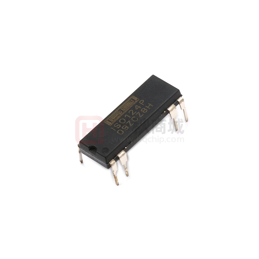
ISO124
SBOS074E – SEPTEMBER 1997 – REVISED JUNE 2018
ISO124 ±10-V Input, Precision Isolation Amplifier
1 Features
3 Description
•
•
•
•
•
•
•
•
The ISO124 is a precision isolation amplifier
incorporating a novel duty cycle modulationdemodulation technique. The signal is transmitted
digitally across a 2-pF differential capacitive barrier.
With digital modulation, the barrier characteristics do
not affect signal integrity, thus resulting in excellent
reliability and good high-frequency transient immunity
across the barrier. Both barrier capacitors are
imbedded in the plastic body of the package.
1
100% Tested for High-Voltage Breakdown
Rated 1500 Vrms
High IMR: 140 dB at 60 Hz
Maximum Nonlinearity: 0.010%
Bipolar Operation: VO = ±10 V
Packages: PDIP-16 and SOIC-28
Ease of Use: Fixed Unity Gain Configuration
Supply Range: ±4.5-V to ±18-V
The ISO124 is easy to use. No external components
are required for operation. The key specifications are
0.010% maximum nonlinearity, 50-kHz signal
bandwidth, and 200-µV/°C VOS drift. A power supply
range of ±4.5 V to ±18 V, and quiescent currents of
±5 mA on VS1 and ±5.5 mA on VS2 make the ISO124
device a good choice for a wide range of applications.
2 Applications
•
•
•
•
•
•
Industrial Process Control:
– Transducer Isolator, Isolator for
Thermocouples, RTDs, Pressure Bridges, and
Flow Meters, 4-mA to 20-mA Loop Isolation
Ground Loop Elimination
Motor and SCR Control
Power Monitoring
PC-Based Data Acquisition
Test Equipment
The ISO124 is available in 16-pin PDIP and 28-lead
SOIC plastic surface-mount packages.
Device Information(1)
PART NUMBER
ISO124
PACKAGE
BODY SIZE (NOM)
PDIP (16)
17.90 mm × 7.50 mm
SOIC (28)
20.01 mm × 6.61 mm
(1) For all available packages, see the package option addendum
at the end of the data sheet.
Simplified Schematic
VIN
VOUT
–VS2
Gnd 2
+VS2
–VS1
Gnd 1
+VS1
1
An IMPORTANT NOTICE at the end of this data sheet addresses availability, warranty, changes, use in safety-critical applications,
intellectual property matters and other important disclaimers. PRODUCTION DATA.
�ISO124
SBOS074E – SEPTEMBER 1997 – REVISED JUNE 2018
www.ti.com
Table of Contents
1
2
3
4
5
6
7
Features ..................................................................
Applications ...........................................................
Description .............................................................
Revision History.....................................................
Pin Configuration and Functions .........................
Specifications.........................................................
1
1
1
2
3
4
6.1
6.2
6.3
6.4
6.5
6.6
4
4
4
4
5
6
Absolute Maximum Ratings ......................................
ESD Ratings..............................................................
Recommended Operating Conditions ......................
Thermal Information ..................................................
Electrical Characteristics...........................................
Typical Characteristics ..............................................
Detailed Description .............................................. 8
7.1
7.2
7.3
7.4
Overview ...................................................................
Functional Block Diagram .........................................
Feature Description...................................................
Device Functional Modes..........................................
8
9
9
9
8
Application and Implementation ........................ 10
8.1 Application Information............................................ 10
8.2 Typical Applications ................................................ 11
9
Power Supply Recommendations...................... 19
9.1 Signal and Supply Connections .............................. 19
10 Layout................................................................... 20
10.1 Layout Guidelines ................................................. 20
10.2 Layout Example .................................................... 20
11 Device and Documentation Support ................. 21
11.1
11.2
11.3
11.4
11.5
11.6
Documentation Support .......................................
Receiving Notification of Documentation Updates
Community Resources..........................................
Trademarks ...........................................................
Electrostatic Discharge Caution ............................
Glossary ................................................................
21
21
21
21
21
21
12 Mechanical, Packaging, and Orderable
Information ........................................................... 21
4 Revision History
Changes from Revision D (July 2016) to Revision E
Page
•
Changed 16-pin SOIC package to 16-pin PDIP package to match content shown in package option addendum at
the end of the data sheet........................................................................................................................................................ 1
•
Changed DVA and NVF pin configuration labels to match content shown in the package option addendum at the
end of the data sheet.............................................................................................................................................................. 3
•
Changed parameter name from "vs temperature" to "Input offset drift" in Electrical Characteristics table............................ 5
•
Changed parameter name from "vs power supply" to "Power-supply rejection ratio" in Electrical Characteristics table ...... 5
•
Changed location of supply voltage specifications from the Electrical Characteristics table to the Recommended
Operating Conditions table ..................................................................................................................................................... 5
•
Changed parameter name from "Quiescent current" to "High-side analog supply current", and changed symbol from
"VS1" to "IVS1" in Electrical Characteristics table ..................................................................................................................... 5
•
Changed parameter name from "Quiescent current" to "Low-side analog supply current", and changed symbol from
"VS2" to "IVS2" in Electrical Characteristics table ..................................................................................................................... 5
•
Changed location of Temperature specifications from the Electrical Characteristics table to the Recommended
Operating Conditions table ..................................................................................................................................................... 5
•
Deleted Thermal resistance parameters from Electrical Characteristics table; see Thermal Information table..................... 5
Changes from Revision C (September 2005) to Revision D
•
2
Page
Added ESD Ratings table, Feature Description section, Device Functional Modes, Application and Implementation
section, Power Supply Recommendations section, Layout section, Device and Documentation Support section, and
Mechanical, Packaging, and Orderable Information section. ................................................................................................ 1
Submit Documentation Feedback
Copyright © 1997–2018, Texas Instruments Incorporated
Product Folder Links: ISO124
�ISO124
www.ti.com
SBOS074E – SEPTEMBER 1997 – REVISED JUNE 2018
5 Pin Configuration and Functions
NVF Package
16-Pin PDIP
Top View
DVA Package
28-Pin SOIC
Top View
+VS1
1
16
Gnd 1
+VS1
1
28
Gnd 1
–VS1
2
15
VIN
–VS1
2
27
VIN
VOUT
7
10
–VS2
VOUT
13
16
–VS2
Gnd 2
8
9
+VS2
Gnd 2
14
15
+VS2
Pin Functions
PIN
I/O
DESCRIPTION
NAME
PDIP
SOIC
Gnd 1
16
28
—
High-side ground reference
Gnd 2
8
14
—
Low-side ground reference
VIN
15
27
I
High-side analog input
VOUT
7
13
O
Low-side analog output
+VS1
1
1
—
High-side positive analog supply
–VS1
2
2
—
High-side negative analog supply
+VS2
9
15
—
Low-side positive analog supply
–VS2
10
16
—
Low-side negative analog supply
Submit Documentation Feedback
Copyright © 1997–2018, Texas Instruments Incorporated
Product Folder Links: ISO124
3
�ISO124
SBOS074E – SEPTEMBER 1997 – REVISED JUNE 2018
www.ti.com
6 Specifications
6.1 Absolute Maximum Ratings
over operating free-air temperature range (unless otherwise noted)
(1)
MIN
Supply voltage
MAX
UNIT
±18
V
Analog input voltage, VIN
100
V
Continuous isolation voltage
1500
Vrms
Junction temperature
125
°C
Output short to common
Continuous
Storage temperature, Tstg
(1)
–40
125
°C
Stresses beyond those listed under Absolute Maximum Ratings may cause permanent damage to the device. These are stress ratings
only, which do not imply functional operation of the device at these or any other conditions beyond those indicated under Recommended
Operating Conditions. Exposure to absolute-maximum-rated conditions for extended periods may affect device reliability.
6.2 ESD Ratings
VALUE
V(ESD)
(1)
(2)
Electrostatic discharge
Human body model (HBM), per ANSI/ESDA/JEDEC JS-001 (1)
±1000
Charged-device model (CDM), per JEDEC specification JESD22-C101 (2)
±500
UNIT
V
JEDEC document JEP155 states that 500-V HBM allows safe manufacturing with a standard ESD control process.
JEDEC document JEP157 states that 250-V CDM allows safe manufacturing with a standard ESD control process.
6.3 Recommended Operating Conditions
over operating free-air temperature range (unless otherwise noted)
MIN
NOM
MAX
UNIT
VS1
High-side analog supply voltage (±VS1 to GND1)
±4.5
±15
±18
V
VS2
Low-side analog supply voltage (±VS2 to GND2)
±4.5
±15
±18
V
VIN
Analog input voltage
TA
Operating temperature
±10
V
–25
85
°C
6.4 Thermal Information
ISO124
THERMAL METRIC
(1)
DVA (SOIC)
NVF (PDIP)
28 PINS
16 PINS
UNIT
RθJA
Junction-to-ambient thermal resistance
79.8
51.0
°C/W
RθJC(top)
Junction-to-case (top) thermal resistance
32.9
32.4
°C/W
RθJB
Junction-to-board thermal resistance
42.2
29.5
°C/W
ψJT
Junction-to-top characterization parameter
6.6
10.4
°C/W
ψJB
Junction-to-board characterization parameter
40.9
29.0
°C/W
(1)
4
For more information about traditional and new thermal metrics, see the Semiconductor and IC Package Thermal Metrics application
report.
Submit Documentation Feedback
Copyright © 1997–2018, Texas Instruments Incorporated
Product Folder Links: ISO124
�ISO124
www.ti.com
SBOS074E – SEPTEMBER 1997 – REVISED JUNE 2018
6.5 Electrical Characteristics
at TA = +25°C , VS1 = VS2 = ±15 V, and RL = 2 kΩ (unless otherwise noted)
PARAMETER
TEST CONDITIONS
MIN
TYP
MAX
UNIT
ISOLATION
Rated voltage
Continuous ac 60 Hz
1500
100% test (1)
Test time = 1 s, partial discharge ≤ 5 pC
2400
Isolation mode rejection
60 Hz
Vac
Vac
140
14
Barrier impedance
10
dB
|| 2
Leakage current at 60 Hz
VISO = 240 Vrms
0.18
Nominal gain
VO = ±10 V
1
Gain error
VO = ±10 V
±0.05
Ω || pF
0.5
µArms
±0.50
%FSR
GAIN
Gain vs temperature
Nonlinearity
V/V
±10
(2)
ppm/°C
±0.005
±0.010
±20
±50
%FSR
INPUT OFFSET VOLTAGE
Initial offset
Input offset drift
PSR
R
Power-supply rejection ratio
Noise
mV
±200
µV/°C
±2
mV/V
4
µV/√Hz
INPUT
Input voltage
±10
Resistance
±12.5
V
200
kΩ
OUTPUT
Output voltage
Current drive
Capacitive load drive
Ripple voltage
(3)
±10
±12.5
±5
±15
mA
V
0.1
µF
20
mVp-p
50
kHz
FREQUENCY RESPONSE
Small-signal bandwidth
Slew rate
2
V/µs
Settling Time 0.10%
VO = ±10 V
50
µs
Settling Time 0.01%
VO = ±10 V
350
µs
150
µs
Overload recovery time
POWER SUPPLIES
IVS1
High-side analog supply current
±5.0
±7.0
mA
IVS2
Low-side analog supply current
±5.5
±7.0
mA
(1)
(2)
(3)
Tested at 1.6x rated, fail on 5-pC partial discharge.
Nonlinearity is the peak deviation of the output voltage from the best-fit straight line, and is expressed as the ratio of deviation to FSR.
Ripple frequency is at carrier frequency (500 kHz).
Submit Documentation Feedback
Copyright © 1997–2018, Texas Instruments Incorporated
Product Folder Links: ISO124
5
�ISO124
SBOS074E – SEPTEMBER 1997 – REVISED JUNE 2018
www.ti.com
6.6 Typical Characteristics
+10
Output Voltage (V)
Output Voltage (V)
at TA = +25°C, and VS = ±15 V (unless otherwise noted)
0
–10
0
500
+10
0
–10
0
1000
50
f = 20 kHz
f = 2 kHz
Figure 2. Sine Response
Figure 1. Sine Response
+10
Output Voltage (V)
Output Voltage (V)
100
Time (µs)
Time (µs)
0
–10
0
500
+10
0
–10
1000
50
0
Time (µs)
100
Time (µs)
Figure 3. Step Response
Figure 4. Step Response
160
Max DC Rating
140
1k
120
Degraded
Performance
IMR (dB)
Peak Isolation Voltage
2.1k
100
80
Typical
Performance
60
0
40
100
6
100
1k
10k
100k
1M
10M
100M
1
10
100
1k
10k
Frequency (Hz)
Frequency (Hz)
Figure 5. Isolation Voltage vs Frequency
Figure 6. IMR vs Frequency
Submit Documentation Feedback
100k
1M
Copyright © 1997–2018, Texas Instruments Incorporated
Product Folder Links: ISO124
�ISO124
www.ti.com
SBOS074E – SEPTEMBER 1997 – REVISED JUNE 2018
Typical Characteristics (continued)
at TA = +25°C, and VS = ±15 V (unless otherwise noted)
60
100mA
54
Leakage Current (rms)
PSRR (dB)
10mA
40
+VS1, +VS2
–VS1, –VS2
20
1mA
1500Vrms
100µA
10µA
240Vrms
1µA
0
0.1µA
10
100
1k
10k
100k
1M
1
10
100
Frequency (Hz)
Figure 7. PSRR vs Frequency
10k
100k
1M
Figure 8. Isolation Leakage Current vs Frequency
100kHz
VOUT/VIN
Frequency
Out
0
VOUT/VIN (dBm)
1k
Frequency (Hz)
250
–10
200
–20
150
–30
100
–40
50
0
500k
1M
Frequency Out
1
1.5M
Input Frequency (Hz)
NOTE: Shaded area shows aliasing frequencies that cannot
be removed by a low-pass filter at the output.
Figure 9. Signal Response to Inputs Greater than 250 kHz
Submit Documentation Feedback
Copyright © 1997–2018, Texas Instruments Incorporated
Product Folder Links: ISO124
7
�ISO124
SBOS074E – SEPTEMBER 1997 – REVISED JUNE 2018
www.ti.com
7 Detailed Description
7.1 Overview
The ISO124 isolation amplifier uses an input and an output section galvanically isolated by matched 1-pF
isolating capacitors built into the plastic package. The input is duty-cycle modulated and transmitted digitally
across the barrier. The output section receives the modulated signal, converts it back to an analog voltage and
removes the ripple component inherent in the demodulation. Input and output sections are fabricated, then laser
trimmed for exceptional circuitry matching common to input and output sections. The sections are then mounted
on opposite ends of the package with the isolating capacitors mounted between the two sections. The ISO124
contains 250 transistors.
7.1.1 Modulator
An input amplifier (A1, as shown in Functional Block Diagram) integrates the difference between the input current
(VIN/200 kΩ) and a switched ±100-µA current source. This current source is implemented by a switchable 200-µA
source and a fixed 100-µA current sink. To understand the basic operation of the modulator, assume that VIN = 0
V. The integrator will ramp in one direction until the comparator threshold is exceeded. The comparator and
sense amp will force the current source to switch; the resultant signal is a triangular waveform with a 50% duty
cycle. The internal oscillator forces the current source to switch at 500 kHz. The resultant capacitor drive is a
complementary duty-cycle modulation square wave
7.1.2 Demodulator
The sense amplifier detects the signal transitions across the capacitive barrier and drives a switched current
source into integrator A2. The output stage balances the duty-cycle modulated current against the feedback
current through the 200-kΩ feedback resistor, resulting in an average value at the VOUT pin equal to VIN. The
sample-and-hold amplifiers in the output feedback loop serve to remove undesired ripple voltages inherent in the
demodulation process.
8
Submit Documentation Feedback
Copyright © 1997–2018, Texas Instruments Incorporated
Product Folder Links: ISO124
�ISO124
www.ti.com
SBOS074E – SEPTEMBER 1997 – REVISED JUNE 2018
7.2 Functional Block Diagram
Isolation Barrier
200µA
200µA
1pF
1pF
1pF
Sense
1pF
100µA
100µA
Sense
150pF
200kΩ
200kΩ
150pF
VIN
VOUT
A2
A1
S/H
G=1
S/H
G=6
Osc
+VS1
Gnd 1
–VS1
+VS2
Gnd 2
–VS2
7.3 Feature Description
7.3.1 Isolation Amplifier
The ISO124 is a precision analog isolation amplifier. The input signal is transmitted digitally across a high-voltage
differential capacitive barrier. With digital modulation, the barrier characteristics do affect signal integrity, resulting
in excellent reliability and high-frequency transient immunity.
7.4 Device Functional Modes
The ISO124 device does not have any additional functional modes.
Submit Documentation Feedback
Copyright © 1997–2018, Texas Instruments Incorporated
Product Folder Links: ISO124
9
�ISO124
SBOS074E – SEPTEMBER 1997 – REVISED JUNE 2018
www.ti.com
8 Application and Implementation
NOTE
Information in the following applications sections is not part of the TI component
specification, and TI does not warrant its accuracy or completeness. TI’s customers are
responsible for determining suitability of components for their purposes. Customers should
validate and test their design implementation to confirm system functionality.
8.1 Application Information
8.1.1 Carrier Frequency Considerations
The ISO124 amplifier transmits the signal across the isolation barrier by a 500-kHz duty-cycle modulation
technique. For input signals having frequencies below 250 kHz, this system works like any linear amplifier. But
for frequencies above 250 kHz, the behavior is similar to that of a sampling amplifier. Figure 9 shows this
behavior graphically; at input frequencies above 250 kHz, the device generates an output signal component of
reduced magnitude at a frequency below 250 kHz. This is the aliasing effect of sampling at frequencies less than
two times the signal frequency (the Nyquist frequency). At the carrier frequency and its harmonics, both the
frequency and amplitude of the aliasing go to zero.
8.1.2 Isolation Mode Voltage Induced Errors
IMV can induce errors at the output as indicated by the plots of IMV vs Frequency. It should be noted that if the
IMV frequency exceeds 250 kHz, the output also will display spurious outputs (aliasing) in a manner similar to
that for VIN > 250 kHz and the amplifier response will be identical to that shown in Figure 9.This occurs because
IMV-induced errors behave like input-referred error signals. To predict the total error, divide the isolation voltage
by the IMR shown in Figure 11 and compute the amplifier response to this input-referred error signal from the
data shown in Figure 9. For example, if a 800-kHz 1000-Vrms IMR is present, then a total of [(–60 dB) + (–30
dB)] x (1000 V) = 32-mV error signal at 200 kHz plus a 1-V, 800-kHz error signal will be present at the output.
8.1.3 High IMV dV/dt Errors
As the IMV frequency increases and the dV/dt exceeds 1000 Vµs, the sense amp may start to false trigger, and
the output will display spurious errors. The common-mode current being sent across the barrier by the high slew
rate is the cause of the false triggering of the sense amplifier. Lowering the power-supply voltages below ±15 V
may decrease the dV/dt to 500 V/M s for typical performance.
8.1.4 High Voltage Testing
TI has adopted a partial discharge test criterion that conforms to the German VDE0884 Optocoupler Standards.
This method requires the measurement of minute current pulses (< 5 pC) while applying 2400-Vrms, 60-Hz highvoltage stress across every ISO124 isolation barrier. No partial discharge may be initiated to pass this test. This
criterion confirms transient overvoltage (1.6 × 1500 Vrms) protection without damage to the ISO124. Lifetest
results verify the absence of failure under continuous rated voltage and maximum temperature.
This new test method represents the “state-of-the art” for nondestructive high-voltage reliability testing. It is
based on the effects of nonuniform fields that exist in heterogeneous dielectric material during barrier
degradation. In the case of void nonuniformities, electric field stress begins to ionize the void region before
bridging the entire high-voltage barrier. The transient conduction of charge during and after the ionization can be
detected externally as a burst of 0.01–0.1-µs current pulses that repeat on each ac voltage cycle. The minimum
ac barrier voltage that initiates partial discharge is defined as the “inception voltage.” Decreasing the barrier
voltage to a lower level is required before partial discharge ceases and is defined as the “extinction voltage.” The
package insulation processes have been characterized and developed to yield an inception voltage in excess of
2400 Vrms so that transient overvoltages below this level will not damage the ISO124. The extinction voltage is
above 1500 Vrms so that even overvoltage induced partial discharge will cease once the barrier voltage is
reduced to the 1500-Vrms (rated) level. Older high-voltage test methods relied on applying a large enough
overvoltage (above rating) to break down marginal parts, but not so high as to damage good ones. Our new
partial discharge testing gives us more confidence in barrier reliability than breakdown/no breakdown criteria.
10
Submit Documentation Feedback
Copyright © 1997–2018, Texas Instruments Incorporated
Product Folder Links: ISO124
�ISO124
www.ti.com
SBOS074E – SEPTEMBER 1997 – REVISED JUNE 2018
8.2 Typical Applications
8.2.1 Output Filters
C2
1000pF
Isolation Barrier
R2
9.76kΩ
R1
4.75kΩ
VIN
OPA237
VOUT = VIN
ISO124
–VS2
C1
220pF
+VS2
Gnd2
Gnd1
–VS1
+VS1
10µH
10µH
±VS1
10µH
10µH
1µF
±VS2
1µF
1µF 1µF 1µF
1µF 1µF 1µF
For more information concerning output filters, see Simple Output Filter Elminiates ISO Amp Output Ripple and Keeps
Full Bandwidth and FilterPro™ MFB and Sallen-Key Low-Pass Filter Design Program User Guide.
Figure 10. ISO124 With Output Filter for Improved Ripple
8.2.1.1 Design Requirements
The ISO124 isolation amplifiers (ISO amps) have a small (10 to 20 mVp-p typical) residual demodulator ripple at
the output. A simple filter can be added to eliminate the output ripple without decreasing the 50kHz signal
bandwidth of the ISO amp.
8.2.1.2 Detailed Design Procedure
The ISO124 device is designed to have a 50-kHz single-pole (Butterworth) signal response. By cascading the
ISO amp with a simple 50-kHz, Q = 1, two-pole, low-pass filter, the overall signal response becomes three-pole
Butterworth. The result is a maximally flat 50-kHz magnitude response and the output ripple reduced below the
noise level. Figure 10 shows the complete circuit. The two-pole filter is a unity-gain Sallen-Key type consisting of
A1, R1, R2, C1, and C2. The values shown give Q = 1 and f–3dB bandwidth = 50 kHz. Because the op amp is
connected as a unity-gain follower, gain and gain accuracy of the ISO amp are unaffected. Using a precision op
amp such as the OPA602 also preserves the DC accuracy of the ISO amp.
Submit Documentation Feedback
Copyright © 1997–2018, Texas Instruments Incorporated
Product Folder Links: ISO124
11
�ISO124
SBOS074E – SEPTEMBER 1997 – REVISED JUNE 2018
www.ti.com
Typical Applications (continued)
8.2.1.3 Application Curves
+3
0
Gain (dB)
–3
1
–9
2
–15
–21
–27
2k
5k
10k
20k
50k
Frequency (Hz)
100k
200k
1) Standard ISO124 has 50kHz single-pole (Butterworth) response.
2) ISO124 with cascaded 50kHz, Q = 1, two-pole, low-pass
filter has three-pole Butterworth response.
12
Figure 11. Gain vs. Frequency
Figure 12. Standard ISO124 (Approximately 20-mVp-p
Output Ripple)
Figure 13. Filtered ISO124 (No Visible Output Ripple)
Figure 14. Step Response of Standard ISO124
Figure 15. Step Response of ISO124 With Added Twopole
Output Filter
Figure 16. Large-signal, 10-kHz Sine-wave Response of
ISO124 With and Without Output Filter
Submit Documentation Feedback
Copyright © 1997–2018, Texas Instruments Incorporated
Product Folder Links: ISO124
�ISO124
www.ti.com
SBOS074E – SEPTEMBER 1997 – REVISED JUNE 2018
Typical Applications (continued)
8.2.2 Battery Monitor
Figure 17 provides a means to monitor the cell voltage on a 600-V battery stack by using the battery as a power
source for the isolated voltage.
This Section Repeated 49 Times.
ISO124
+V
10kΩ
1
e1 = 12V
10kΩ
9
V=
e1
7
15
2
8
10
e2 = 12V
2
16
Multiplexer
–V
Charge/Discharge Control
ISO124
+V –V
+V
e49 = 12V
15
7
1
4
INA105
9
e50 = 12V
Control
Section
10kΩ
10
25kΩ
7
5
2
8
25kΩ
2
10kΩ
16
6
–V
25kΩ
3
1
V=
e50
2
25kΩ
(Derives input power from the battery.)
Figure 17. Battery Monitor for a 600-V Battery Power System
Submit Documentation Feedback
Copyright © 1997–2018, Texas Instruments Incorporated
Product Folder Links: ISO124
13
�ISO124
SBOS074E – SEPTEMBER 1997 – REVISED JUNE 2018
www.ti.com
Typical Applications (continued)
8.2.3 Programmable Gain Amplifier
In applications where variable gain configurations are required, a programmable gain amplifier like the PGA102
can be used with the ISO124 device. Figure 18 uses an ISO150 device to provide gain pin selection options to
the PGA102 device.
A0
A1
ISO150
+15V– 15V
+15V –15V
1
2
1
9
6
2
VIN
15
7
PGA102
8
5
4
3
10
15
ISO124
7
VOUT
8
16
Figure 18. Programmable-Gain Isolation Channel With Gains of 1, 10, and 100
14
Submit Documentation Feedback
Copyright © 1997–2018, Texas Instruments Incorporated
Product Folder Links: ISO124
�ISO124
www.ti.com
SBOS074E – SEPTEMBER 1997 – REVISED JUNE 2018
Typical Applications (continued)
8.2.4 Thermocouple Amplifier
For isolated temperature measurements, Figure 19 provides an application solution using the INA114 or INA128
devices, feeding the input stage of the ISO124 device. The table provides suggested resistor values based on
the type of thermistor used in the application.
+15V
2
10.0V
6
Thermocouple
REF102
R4
R1
27kΩ
+15V –15V +15V –15V
+15V
Isothermal
Block with
1N4148(1)
1
2
2
7
+In
INA114
or
INA128
1
RG
1MΩ
4
R2
8
ISO124
9
6
10
15
7
VOUT
8
5
–In
4
16
3
R5
50Ω
R3
100Ω
–15V
R6
100
Zero Adj
ISA
TYPE
E
Ground Loop Through Conduit
J
NOTE: (1) –2.1mV/°C at 2.00µA.
K
T
MATERIAL
Chromel
Constantan
Iron
Constantan
Chromel
Alumel
Copper
Constantan
SEEBACK
COEFFICIENT
(µV/°C)
R2
(R3 = 100Ω)
R4
(R5 + R6 = 100Ω)
58.5
3.48kΩ
56.2kΩ
50.2
4.12kΩ
64.9kΩ
39.4
5.23kΩ
80.6kΩ
38.0
5.49kΩ
84.5kΩ
Figure 19. Thermocouple Amplifier With Ground Loop Elimination,
Cold Junction Compensation, and Up-scale Burn-out
Submit Documentation Feedback
Copyright © 1997–2018, Texas Instruments Incorporated
Product Folder Links: ISO124
15
�ISO124
SBOS074E – SEPTEMBER 1997 – REVISED JUNE 2018
www.ti.com
Typical Applications (continued)
8.2.5 Isolated 4-mA to 20-mA Instrument Loop
For isolated temperature measurements in a 4-mA to 20-mA loop, Figure 20 provides a solution using the
XTR101 and RCV420 devices. A high-performance PT100 resistance temperature detector (RTD) provides the
user with an isolated 0-V to 5-V representation of the isolated temperature measurement.
1
13
0.8mA
0.8mA
14
10
4-20mA
3
RG
+VS = 15V on PWS740
0.01µF
XTR105
4
2
RTD
(PT100)
ISO124
+V
16
7
1
3
6
15
14
2 RCV420
5, 13
10
4
11
RZ(1)
RCM
1kΩ
15
9
7
8
10
12
VOUT
0V - 5V
2
16
1.6mA
–V
Gnd
–VS = –15V
on PWS740
Figure 20. Isolated 4- to 20-mA Instrument Loop (RTD Shown)
8.2.6 Single-Supply Operation of the ISO124 Isolation Amplifier
The circuit shown in Figure 21 uses a 5.1-V Zener diode to generate the negative supply for an ISO12x from a
single supply on the high-voltage side of the isolation amplifier. The input measuring range will be dependent on
the applied voltage as noted in the accompanying table.
VS1 (+15V)
7
VS
(V)
INPUT RANGE
(V)(1)
20+
15
12
–2 to +10
–2 to +5
–2 to +2
INA105
Difference Amp
2
5
R1
10kΩ
1
6
Signal Source
VIN
+
RS
R3
3
+VS2 (+15V)
R2
R4
15
RC
Gnd
Reference
VOUT = VIN
8
16
4
7
ISO124
(1)
1
9
In
10
Com 2
2
IN4689
5.1V
–VS1
–VS2 (–15V)
NOTE: Because the amplifier is unity gain, the input range is also the output range. The output can go to –2 V because the
output section of the ISO amp operates from dual supplies.
For additional information see Single-Supply Operation of Isolation Amplifiers.
Figure 21. Single-Supply Operation of the ISO124 Isolation Amplifier Schematic
16
Submit Documentation Feedback
Copyright © 1997–2018, Texas Instruments Incorporated
Product Folder Links: ISO124
�ISO124
www.ti.com
SBOS074E – SEPTEMBER 1997 – REVISED JUNE 2018
Typical Applications (continued)
8.2.7 Input-Side Powered ISO Amplifier
The user side of the ISO124 device can be powered from the high voltage side using an isolated DC-DC
converter as shown in Figure 22.
1
2
5
6
7
DCP011515DB
or
DCV011515D
0.47µF
0.47µF
0.47µF
VIN
Input
Gnd
–15V, 20mA
16
10
15
Gnd VIN
Input
Section
V+
+15V
1
V–
2
V–
ISO124
+15V, 20mA
9
Auxiliary
Isolated
Power
Output
V+
Output
Section
VO
7
Gnd
8
Output
Gnd
–15V
VO
Figure 22. Input-Side Powered ISO Amplifier Schematic
Submit Documentation Feedback
Copyright © 1997–2018, Texas Instruments Incorporated
Product Folder Links: ISO124
17
�ISO124
SBOS074E – SEPTEMBER 1997 – REVISED JUNE 2018
www.ti.com
Typical Applications (continued)
8.2.8 Powered ISO Amplifier With Three-Port Isolation
Figure 23 illustrates an application solution that provides isolated power to both the user and high-voltage sides
of the ISO124 amplifier.
+15V Gnd
1
DCP011515DB
or
DCV011515D
7
6
5
2
5
7
DCP011515DB
or
DCV011515D
2
1
0.47µF
0.47µF
6
0.47µF
0.47µF
0.47µF
VIN
–15V, 20mA
Input
Gnd
16
10
15
Gnd VIN
Input
Section
Auxiliary
Isolated
Power
Output
V+
1
+15V, 20mA
V–
2
V–
ISO124
+15V, 20mA
9
Auxiliary
Isolated
Power
Output
V+
Output
Section
VO
7
Gnd
8
Output
Gnd
–15V, 20mA
VO
Figure 23. Powered ISO Amplifier With Three-Port Isolation Schematic
18
Submit Documentation Feedback
Copyright © 1997–2018, Texas Instruments Incorporated
Product Folder Links: ISO124
�ISO124
www.ti.com
SBOS074E – SEPTEMBER 1997 – REVISED JUNE 2018
9 Power Supply Recommendations
9.1 Signal and Supply Connections
Each power-supply pin should be bypassed with 1-µF tantalum capacitors located as close to the amplifier as
possible. The internal frequency of the modulator/demodulator is set at 500 kHz by an internal oscillator.
Therefore, if it is desired to minimize any feedthrough noise (beat frequencies) from a DC-DC converter, use a π
filter on the supplies (see Figure 10). The ISO124 output has a 500-kHz ripple of 20 mV, which can be removed
with a simple 2-pole low-pass filter with a 100-kHz cutoff using a low-cost op amp (see Figure 10).
The input to the modulator is a current (set by the 200-kΩ integrator input resistor) that makes it possible to have
an input voltage greater than the input supplies, as long as the output supply is at least ±15 V. It is therefore
possible, when using an unregulated DC-DC converter, to minimize PSR related output errors with ±5-V voltage
regulators on the isolated side and still get the full ±10-V input and output swing.
Isolation Barrier
VIN
ISO124
–VS2
VOUT
Gnd
Gnd
+VS2
–VS1
+VS1
±VS1
1µF
1µF 1µF
±VS2
1µF
Figure 24. Basic Signal and Power Connections
Submit Documentation Feedback
Copyright © 1997–2018, Texas Instruments Incorporated
Product Folder Links: ISO124
19
�ISO124
SBOS074E – SEPTEMBER 1997 – REVISED JUNE 2018
www.ti.com
10 Layout
10.1 Layout Guidelines
To maintain the isolation barrier of the device, the distance between the high-side ground (pin 16 or 28) and the
low-side ground (pin 8 or 14) should be kept at maximum; that is, the entire area underneath the device should
be kept free of any conducting materials.
10.2 Layout Example
Top View
1 µF
SMD
0603
1 µF
1
+VS1
GND
VIN
-VS1
SMD
0603
ISOLATION
BOUNDARY
ISOLATION
BOUNDARY
ISO124
1 µF
VOUT
-VS2
GND
+VS2
SMD
0603
LEGEND
TOP layer:
copper pour & traces
1 µF
GND
SMD
0603
via to ground plane
Figure 25. ISO124 Layout Example
20
Submit Documentation Feedback
Copyright © 1997–2018, Texas Instruments Incorporated
Product Folder Links: ISO124
�ISO124
www.ti.com
SBOS074E – SEPTEMBER 1997 – REVISED JUNE 2018
11 Device and Documentation Support
11.1 Documentation Support
11.1.1 Related Documentation
For related documentation see the following:
• Single-Supply Operation of Isolation Amplifiers.
• Simple Output Filter Eliminates ISO Amp Output Ripple and Keeps Full Bandwidth.
• FilterPro™ User's Guide.
11.2 Receiving Notification of Documentation Updates
To receive notification of documentation updates, navigate to the device product folder on ti.com. In the upper
right corner, click on Alert me to register and receive a weekly digest of any product information that has
changed. For change details, review the revision history included in any revised document.
11.3 Community Resources
The following links connect to TI community resources. Linked contents are provided "AS IS" by the respective
contributors. They do not constitute TI specifications and do not necessarily reflect TI's views; see TI's Terms of
Use.
TI E2E™ Online Community TI's Engineer-to-Engineer (E2E) Community. Created to foster collaboration
among engineers. At e2e.ti.com, you can ask questions, share knowledge, explore ideas and help
solve problems with fellow engineers.
Design Support TI's Design Support Quickly find helpful E2E forums along with design support tools and
contact information for technical support.
11.4 Trademarks
FilterPro, E2E are trademarks of Texas Instruments.
All other trademarks are the property of their respective owners.
11.5 Electrostatic Discharge Caution
This integrated circuit can be damaged by ESD. Texas Instruments recommends that all integrated circuits be handled with
appropriate precautions. Failure to observe proper handling and installation procedures can cause damage.
ESD damage can range from subtle performance degradation to complete device failure. Precision integrated circuits may be more
susceptible to damage because very small parametric changes could cause the device not to meet its published specifications.
11.6 Glossary
SLYZ022 — TI Glossary.
This glossary lists and explains terms, acronyms, and definitions.
12 Mechanical, Packaging, and Orderable Information
The following pages include mechanical, packaging, and orderable information. This information is the most
current data available for the designated devices. This data is subject to change without notice and revision of
this document. For browser-based versions of this data sheet, refer to the left-hand navigation.
Submit Documentation Feedback
Copyright © 1997–2018, Texas Instruments Incorporated
Product Folder Links: ISO124
21
�PACKAGE OPTION ADDENDUM
www.ti.com
10-Dec-2020
PACKAGING INFORMATION
Orderable Device
Status
(1)
Package Type Package Pins Package
Drawing
Qty
Eco Plan
(2)
Lead finish/
Ball material
MSL Peak Temp
Op Temp (°C)
Device Marking
(3)
(4/5)
(6)
ISO124P
ACTIVE
PDIP
NVF
8
25
RoHS &
Non-Green
NIPDAU
N / A for Pkg Type
-25 to 85
ISO124P
ISO124U
ACTIVE
SOIC
DVA
8
20
RoHS & Green
NIPDAU
Level-3-260C-168 HR
-25 to 85
ISO
124U
ISO124U/1K
ACTIVE
SOIC
DVA
8
1000
RoHS & Green
NIPDAU
Level-3-260C-168 HR
-25 to 85
ISO
124U
ISO124U/1KE4
ACTIVE
SOIC
DVA
8
1000
RoHS & Green
NIPDAU
Level-3-260C-168 HR
-25 to 85
ISO
124U
ISO124UE4
ACTIVE
SOIC
DVA
8
20
RoHS & Green
NIPDAU
Level-3-260C-168 HR
-25 to 85
ISO
124U
(1)
The marketing status values are defined as follows:
ACTIVE: Product device recommended for new designs.
LIFEBUY: TI has announced that the device will be discontinued, and a lifetime-buy period is in effect.
NRND: Not recommended for new designs. Device is in production to support existing customers, but TI does not recommend using this part in a new design.
PREVIEW: Device has been announced but is not in production. Samples may or may not be available.
OBSOLETE: TI has discontinued the production of the device.
(2)
RoHS: TI defines "RoHS" to mean semiconductor products that are compliant with the current EU RoHS requirements for all 10 RoHS substances, including the requirement that RoHS substance
do not exceed 0.1% by weight in homogeneous materials. Where designed to be soldered at high temperatures, "RoHS" products are suitable for use in specified lead-free processes. TI may
reference these types of products as "Pb-Free".
RoHS Exempt: TI defines "RoHS Exempt" to mean products that contain lead but are compliant with EU RoHS pursuant to a specific EU RoHS exemption.
Green: TI defines "Green" to mean the content of Chlorine (Cl) and Bromine (Br) based flame retardants meet JS709B low halogen requirements of