Reference Guide
SLUU470B – December 2010 – Revised June 2011
Isolated, Full-Duplex, 1-Mbps, 3.3-V to 3.3-V RS-485
Interface
1
Circuit Function and Benefits
This circuit provides an isolated, 1-Mbps, 3.3-V to 3.3-V RS-485 interface using the ISO35T, isolated
RS-485 transceiver and the TPS76333 high-accuracy linear regulator. This circuit achieves signal and
power isolation and at the same time decreases board space and power consumption.
4
T1 !
8
3
2
7
6
1
5
U2 !
D1 !
1
C4 C5
3
2
C1
IN
OUT
5
EN
GND NC
C6
1
D2 !
U1 !
1
2
J1
4
VIN
C2
GND1
R
7
8
16
VOUT
C3
GND2
D2
VCC1
GND1
5
RE
D
VCC2
14
R
RE
13
B
B
Z
12
Z
11
Y
Y
15
DE
D
A
A
3
6
DE
D1
GND2
9, 10
!
Indicates components that
may be hot to touch
Figure 1. Isolated, Full-Duplex, 1-Mbps, 3.3-V to 3.3-V RS-485 Interface
2
Circuit Description
The ISO35T is an isolated differential line transceiver with integrated transformer driver that provides the
primary voltage for an isolation transformer. The device is ideal for long transmission lines because the
ground loop is broken to allow the device to operate with a much larger common-mode voltage range. The
symmetrical isolation barrier of each device is tested to provide 2500 Vrms of isolation between the line
transceiver and the logic-level interface.
The galvanically isolated differential bus transceiver is designed for full-duplex data communication on
multipoint bus-transmission lines. The transceiver combines a galvanically isolated differential line driver
and differential-input line receiver.
Any cabled I/O can be subjected to electrical noise transients from various sources. These noise
transients can cause damage to the transceiver and/or nearby sensitive circuitry if they are of sufficient
magnitude and duration. The ISO35T can significantly reduce the risk of data corruption and damage to
expensive control circuits.
The integrated transformer driver consists of an oscillator followed by a flip-flop stage generating two
complementary, 50% duty-cycle square waves. These two signals drive the ground-referenced N-channel
power switches. Internal circuitry ensures break-before-make action between the two switches.
SLUU470B – December 2010 – Revised June 2011
Submit Documentation Feedback
Isolated, Full-Duplex, 1-Mbps, 3.3-V to 3.3-V RS-485 Interface
Copyright © 2010–2011, Texas Instruments Incorporated
1
�Common Variations
www.ti.com
VS
OSC
FF
4.7 mF
Figure 2. Simplified Transformer Driver
A pair of Schottky diodes and a bulk capacitor build a full-wave rectifier providing the input voltage for the
TPS76333 linear voltage regulator.
This low-dropout (LDO) voltage regulator offers the benefits of low dropout voltage, low-power operation,
and miniaturized packaging. The regulator features low dropout voltages and quiescent currents compared
to conventional LDO regulators. Offered in a 5-terminal, small-outline, integrated-circuit SOT-23 package,
the TPS76333 is ideal for cost-sensitive designs and for applications where board space is at a premium.
A combination of new circuit design and process innovation has enabled the usual PNP pass transistor to
be replaced by a PMOS pass element. Because the PMOS pass element behaves as a low-value resistor,
the dropout voltage is very low (typically 300 mV at 150 mA of load current) and is directly proportional to
the load current. Because the PMOS pass element is a voltage-driven device, the quiescent current is
very low (140 µA maximum) and is stable over the entire range of output load current (0 mA to 150 mA).
The TPS76333 also features a logic-enabled sleep mode to shut down the regulator, reducing quiescent
current to 1 µA maximum at TJ = 25°C. The TPS76333 output provides a regulated 3.3-V power supply to
the ISO35T bus-side circuitry (VCC2) as shown in Figure 1.
Although not required, a 0.047-µF or larger ceramic bypass input capacitor, connected between IN and
GND and located close to the TPS763xx, is recommended to improve transient response and noise
rejection. A higher-value electrolytic input capacitor may be necessary if large, fast-rise-time load
transients are anticipated and the device is located several inches from the power source.
Like all low-dropout regulators, the TPS76333 requires an output capacitor connected between OUT and
GND to stabilize the internal loop control. The minimum recommended capacitance value is 4.7 µF and
the equivalent series resistance (ESR) must be between 0.3 Ω and 10 Ω. Capacitor values of 4.7 µF or
larger are acceptable, provided the ESR is less than 10 Ω. Solid tantalum electrolytic, aluminum
electrolytic, and multilayer ceramic capacitors are all suitable, provided they meet the requirements
described previously. Most of the commercially available 4.7-µF surface-mount solid tantalum capacitors,
including devices from Sprague, Kemet, and Nichico, meet the ESR requirements stated previously.
3
Common Variations
Powering the ISO35T requires a 1CT : 1.5CT transformer (T1) to assure sufficient headroom for the
TPS76333 LDO to provide a regulated 3.3-V output. The external transformer used with the ISO35T must
have a center-tapped primary winding. The turns ratio of the transformer must provide the minimum
required output voltage at the maximum anticipated load current with the minimum input voltage. Table 1
lists suitable transformers for the circuit in Figure 1.
Table 1. Recommended Isolation Transformers
Manufacturer
2
1:1.5 Transformer
Coilcraft
DA2303-AL
Murata
782485/55C
Isolated, Full-Duplex, 1-Mbps, 3.3-V to 3.3-V RS-485 Interface
SLUU470B – December 2010 – Revised June 2011
Submit Documentation Feedback
Copyright © 2010–2011, Texas Instruments Incorporated
�Circuit Performance
www.ti.com
4
Circuit Performance
Figure 3 shows a low-frequency sweep for measuring the radiated emissions to demonstrate compliance
with the EN55022 standard, which specifies the limits and methods of measurement of radio disturbance
characteristics of information technology equipment.
Figure 3. Radiated Emissions (dBµV/m) from 10 kHz to 30 MHz
Figure 4 shows the circuit efficiency over load current. Although load currents in the lower 20 mA can be
expected for low data rates and no common-mode voltage, higher load currents around 100 mA are
required for high data rates and high common-mode voltages.
70
60
Efficiency - %
50
40
30
20
10
0
10 20
30 40 50 60 70 80 90 100 110 120 130 140 150 160 170 180 190 200
Load Current - mA
Figure 4. Efficiency Over Load Current
SLUU470B – December 2010 – Revised June 2011
Submit Documentation Feedback
Isolated, Full-Duplex, 1-Mbps, 3.3-V to 3.3-V RS-485 Interface
Copyright © 2010–2011, Texas Instruments Incorporated
3
�Circuit Layout and Bill of Materials
5
www.ti.com
Circuit Layout and Bill of Materials
Figure 5 shows the silk screen as well as the top and bottom layers of the two-layer board, with the actual
dc-dc converter capturing an area of 20 mm × 14 mm only.
Figure 5. Board Layout: Silk Screen (Left), Top Layer (Middle), Bottom Layer (Right)
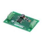
Figure 6 shows a picture of the actual board.
Figure 6. Reference Design Board: Top View
Table 2 shows the final bill of materials.
Table 2. Bill of Materials
Designator
Part No.
Manufacturer
Value
Package/Size
U1
ISO35T
TI
Full-duplex XCVR
DW-16
U2
TPS76333
TI
3.3-V LDO
DBV-5
D1, D2
MBR0520L
Fairchild
0.4-W Schottky diode
SOD123
C2, C3, C5
C0402C104K4RACTU
KEMET
0.1-µF/16V/X7R (ceramic)
0402 (1 × 0,5 mm2)
C1, C4
GRM21BR61C106KE15L
Murata
10-µF/16V/X5R (ceramic)
0805 (2 × 1,25 mm2)
C6
T491A475K016AT
KEMET
4.7-µF/16V (tantalum)
3,2 × 1,6 mm2
T1
DA2303-AL
Coilcraft
1:1.5
10 × 12 mm2
J1, J2
MPT 0,5 / 6-2,54
Phoenix-Contact
6-position terminal block
6,2 × 15,7 mm2
empty para
4
Isolated, Full-Duplex, 1-Mbps, 3.3-V to 3.3-V RS-485 Interface
SLUU470B – December 2010 – Revised June 2011
Submit Documentation Feedback
Copyright © 2010–2011, Texas Instruments Incorporated
�Evaluation Board/Kit Important Notice
Texas Instruments (TI) provides the enclosed product(s) under the following conditions:
This evaluation board/kit is intended for use for ENGINEERING DEVELOPMENT, DEMONSTRATION, OR EVALUATION
PURPOSES ONLY and is not considered by TI to be a finished end-product fit for general consumer use. Persons handling the
product(s) must have electronics training and observe good engineering practice standards. As such, the goods being provided are
not intended to be complete in terms of required design-, marketing-, and/or manufacturing-related protective considerations,
including product safety and environmental measures typically found in end products that incorporate such semiconductor
components or circuit boards. This evaluation board/kit does not fall within the scope of the European Union directives regarding
electromagnetic compatibility, restricted substances (RoHS), recycling (WEEE), FCC, CE or UL, and therefore may not meet the
technical requirements of these directives or other related directives.
Should this evaluation board/kit not meet the specifications indicated in the User’s Guide, the board/kit may be returned within 30
days from the date of delivery for a full refund. THE FOREGOING WARRANTY IS THE EXCLUSIVE WARRANTY MADE BY
SELLER TO BUYER AND IS IN LIEU OF ALL OTHER WARRANTIES, EXPRESSED, IMPLIED, OR STATUTORY, INCLUDING
ANY WARRANTY OF MERCHANTABILITY OR FITNESS FOR ANY PARTICULAR PURPOSE.
The user assumes all responsibility and liability for proper and safe handling of the goods. Further, the user indemnifies TI from all
claims arising from the handling or use of the goods. Due to the open construction of the product, it is the user’s responsibility to
take any and all appropriate precautions with regard to electrostatic discharge.
EXCEPT TO THE EXTENT OF THE INDEMNITY SET FORTH ABOVE, NEITHER PARTY SHALL BE LIABLE TO THE OTHER
FOR ANY INDIRECT, SPECIAL, INCIDENTAL, OR CONSEQUENTIAL DAMAGES.
TI currently deals with a variety of customers for products, and therefore our arrangement with the user is not exclusive.
TI assumes no liability for applications assistance, customer product design, software performance, or infringement of
patents or services described herein.
Please read the User’s Guide and, specifically, the Warnings and Restrictions notice in the User’s Guide prior to handling the
product. This notice contains important safety information about temperatures and voltages. For additional information on TI’s
environmental and/or safety programs, please contact the TI application engineer or visit www.ti.com/esh.
No license is granted under any patent right or other intellectual property right of TI covering or relating to any machine, process, or
combination in which such TI products or services might be or are used.
FCC Warning
This evaluation board/kit is intended for use for ENGINEERING DEVELOPMENT, DEMONSTRATION, OR EVALUATION
PURPOSES ONLY and is not considered by TI to be a finished end-product fit for general consumer use. It generates, uses, and
can radiate radio frequency energy and has not been tested for compliance with the limits of computing devices pursuant to part 15
of FCC rules, which are designed to provide reasonable protection against radio frequency interference. Operation of this
equipment in other environments may cause interference with radio communications, in which case the user at his own expense
will be required to take whatever measures may be required to correct this interference.
EVM Warnings and Restrictions
It is important to operate this EVM within the input voltage range of 0 V to 5.5 V and the output voltage range of 0 V to 6 V.
Exceeding the specified input range may cause unexpected operation and/or irreversible damage to the EVM. If there are
questions concerning the input range, please contact a TI field representative prior to connecting the input power.
Applying loads outside of the specified output range may result in unintended operation and/or possible permanent damage to the
EVM. Please consult the EVM User's Guide prior to connecting any load to the EVM output. If there is uncertainty as to the load
specification, please contact a TI field representative.
During normal operation, some circuit components may have case temperatures greater than 85°C. The EVM is designed to
operate properly with certain components above 85°C as long as the input and output ranges are maintained. These components
include but are not limited to linear regulators, switching transistors, pass transistors, and current sense resistors. These types of
devices can be identified using the EVM schematic located in the EVM User's Guide. When placing measurement probes near
these devices during operation, please be aware that these devices may be very warm to the touch.
Mailing Address: Texas Instruments, Post Office Box 655303, Dallas, Texas 75265
Copyright © 2011, Texas Instruments Incorporated
�IMPORTANT NOTICE
Texas Instruments Incorporated and its subsidiaries (TI) reserve the right to make corrections, modifications, enhancements, improvements,
and other changes to its products and services at any time and to discontinue any product or service without notice. Customers should
obtain the latest relevant information before placing orders and should verify that such information is current and complete. All products are
sold subject to TI’s terms and conditions of sale supplied at the time of order acknowledgment.
TI warrants performance of its hardware products to the specifications applicable at the time of sale in accordance with TI’s standard
warranty. Testing and other quality control techniques are used to the extent TI deems necessary to support this warranty. Except where
mandated by government requirements, testing of all parameters of each product is not necessarily performed.
TI assumes no liability for applications assistance or customer product design. Customers are responsible for their products and
applications using TI components. To minimize the risks associated with customer products and applications, customers should provide
adequate design and operating safeguards.
TI does not warrant or represent that any license, either express or implied, is granted under any TI patent right, copyright, mask work right,
or other TI intellectual property right relating to any combination, machine, or process in which TI products or services are used. Information
published by TI regarding third-party products or services does not constitute a license from TI to use such products or services or a
warranty or endorsement thereof. Use of such information may require a license from a third party under the patents or other intellectual
property of the third party, or a license from TI under the patents or other intellectual property of TI.
Reproduction of TI information in TI data books or data sheets is permissible only if reproduction is without alteration and is accompanied
by all associated warranties, conditions, limitations, and notices. Reproduction of this information with alteration is an unfair and deceptive
business practice. TI is not responsible or liable for such altered documentation. Information of third parties may be subject to additional
restrictions.
Resale of TI products or services with statements different from or beyond the parameters stated by TI for that product or service voids all
express and any implied warranties for the associated TI product or service and is an unfair and deceptive business practice. TI is not
responsible or liable for any such statements.
TI products are not authorized for use in safety-critical applications (such as life support) where a failure of the TI product would reasonably
be expected to cause severe personal injury or death, unless officers of the parties have executed an agreement specifically governing
such use. Buyers represent that they have all necessary expertise in the safety and regulatory ramifications of their applications, and
acknowledge and agree that they are solely responsible for all legal, regulatory and safety-related requirements concerning their products
and any use of TI products in such safety-critical applications, notwithstanding any applications-related information or support that may be
provided by TI. Further, Buyers must fully indemnify TI and its representatives against any damages arising out of the use of TI products in
such safety-critical applications.
TI products are neither designed nor intended for use in military/aerospace applications or environments unless the TI products are
specifically designated by TI as military-grade or "enhanced plastic." Only products designated by TI as military-grade meet military
specifications. Buyers acknowledge and agree that any such use of TI products which TI has not designated as military-grade is solely at
the Buyer's risk, and that they are solely responsible for compliance with all legal and regulatory requirements in connection with such use.
TI products are neither designed nor intended for use in automotive applications or environments unless the specific TI products are
designated by TI as compliant with ISO/TS 16949 requirements. Buyers acknowledge and agree that, if they use any non-designated
products in automotive applications, TI will not be responsible for any failure to meet such requirements.
Following are URLs where you can obtain information on other Texas Instruments products and application solutions:
Products
Applications
Audio
www.ti.com/audio
Communications and Telecom www.ti.com/communications
Amplifiers
amplifier.ti.com
Computers and Peripherals
www.ti.com/computers
Data Converters
dataconverter.ti.com
Consumer Electronics
www.ti.com/consumer-apps
DLP® Products
www.dlp.com
Energy and Lighting
www.ti.com/energy
DSP
dsp.ti.com
Industrial
www.ti.com/industrial
Clocks and Timers
www.ti.com/clocks
Medical
www.ti.com/medical
Interface
interface.ti.com
Security
www.ti.com/security
Logic
logic.ti.com
Space, Avionics and Defense
www.ti.com/space-avionics-defense
Power Mgmt
power.ti.com
Transportation and
Automotive
www.ti.com/automotive
Microcontrollers
microcontroller.ti.com
Video and Imaging
www.ti.com/video
RFID
www.ti-rfid.com
Wireless
www.ti.com/wireless-apps
RF/IF and ZigBee® Solutions
www.ti.com/lprf
TI E2E Community Home Page
e2e.ti.com
Mailing Address: Texas Instruments, Post Office Box 655303, Dallas, Texas 75265
Copyright © 2011, Texas Instruments Incorporated
�