Order
Now
Product
Folder
Support &
Community
Tools &
Software
Technical
Documents
TL071, TL071A, TL071B
TL072, TL072A, TL072B, TL074, TL074A, TL074B, TL072M, TL074M
SLOS080N – SEPTEMBER 1978 – REVISED JULY 2017
TL07xx Low-Noise JFET-Input Operational Amplifiers
1 Features
3 Description
•
•
The TL07xx JFET-input operational amplifiers
incorporate well-matched, high-voltage JFET and
bipolar transistors in a monolithic integrated circuit.
The devices feature high slew rates, low-input bias
and offset currents, and low offset-voltage
temperature coefficient. The low harmonic distortion
and low noise make the TL07x series ideally suited
for high-fidelity and audio pre-amplifier applications.
The TL071 device has offset pins to support external
input offset correction.
1
•
•
•
•
•
•
•
•
•
Low Power Consumption
Wide Common-Mode and Differential Voltage
Ranges
Low Input Bias and Offset Currents
Output Short-Circuit Protection
Low Total Harmonic Distortion: 0.003% (Typical)
Low Noise
Vn = 18 nV/√Hz (Typical) at f = 1 kHz
High-Input Impedance: JFET Input Stage
Internal Frequency Compensation
Latch-Up-Free Operation
High Slew Rate: 13 V/μs (Typical)
Common-Mode Input Voltage Range
Includes VCC+
2 Applications
•
•
•
•
•
•
Motor Integrated Systems: UPS
Drives and Control Solutions: AC Inverter and VF
Drives
Renewables: Solar Inverters
Pro Audio Mixers
DLP Front Projection System
Oscilloscopes
Device Information(1)
PART NUMBER
TL07xxD
PACKAGE
BODY SIZE (NOM)
SOIC (14)
8.65 mm × 3.91 mm
SOIC (8)
4.90 mm x 3.90 mm
TL07xxJG
CDIP (8)
9.59 mm x 6.67 mm
TL074xJ
CDIP (14)
19.56 mm × 6.92 mm
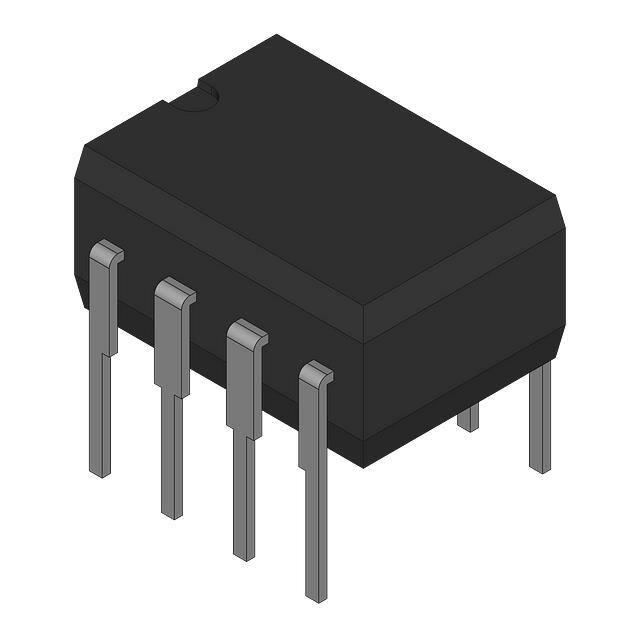
TL07xxP
PDIP (8)
9.59 mm x 6.35 mm
TL07xxPS
SO (8)
6.20 mm x 5.30 mm
TL074xN
PDIP (14)
19.3 mm × 6.35 mm
TL074xNS
SO (14)
10.30 mm × 5.30 mm
TL07xxPW
TSSOP (8)
4.40 mm x 3.00 mm
TL074xPW
TSSOP (14)
5.00 mm × 4.40 mm
(1) For all available packages, see the orderable addendum at
the end of the data sheet.
Logic Symbols
TL071
TL072 (each amplifier)
TL074 (each amplifier)
OFFSET N1
IN+
+
IN+
+
IN−
−
OUT
IN−
OFFSET N2
−
OUT
Copyright © 2017, Texas Instruments Incorporated
1
An IMPORTANT NOTICE at the end of this data sheet addresses availability, warranty, changes, use in safety-critical applications,
intellectual property matters and other important disclaimers. PRODUCTION DATA.
�TL071, TL071A, TL071B
TL072, TL072A, TL072B, TL074, TL074A, TL074B, TL072M, TL074M
SLOS080N – SEPTEMBER 1978 – REVISED JULY 2017
www.ti.com
Table of Contents
1
2
3
4
5
6
Features .................................................................. 1
Applications ........................................................... 1
Description ............................................................. 1
Revision History..................................................... 2
Pin Configuration and Functions ......................... 4
Specifications....................................................... 10
6.1
6.2
6.3
6.4
6.5
6.6
6.7
6.8
6.9
6.10
Absolute Maximum Ratings .................................... 10
ESD Ratings............................................................ 10
Recommended Operating Conditions..................... 10
Thermal Information: TL071x.................................. 11
Thermal Information: TL072x.................................. 11
Thermal Information: TL072x (cont.)....................... 11
Thermal Information: TL074x.................................. 11
Thermal Information: TL074x (cont)........................ 12
Thermal Information: TL074x (cont)........................ 12
Electrical Characteristics: TL071C, TL072C,
TL074C .................................................................... 13
6.11 Electrical Characteristics: TL071AC, TL072AC,
TL074AC .................................................................. 14
6.12 Electrical Characteristics: TL071BC, TL072BC,
TL074BC .................................................................. 15
6.13 Electrical Characteristics: TL071I, TL072I,
TL074I ...................................................................... 16
6.14 Electrical Characteristics: TL071M, TL072M ........ 17
6.15 Electrical Characteristics: TL074M ....................... 18
6.16 Switching Characteristics: TL07xM ....................... 19
6.17 Switching Characteristics: TL07xC, TL07xAC,
TL07xBC, TL07xI ..................................................... 19
6.18 Typical Characteristics .......................................... 20
6.1 Parameter Measurement Information ..................... 25
7
Detailed Description ............................................ 26
7.1
7.2
7.3
7.4
8
Overview .................................................................
Functional Block Diagram .......................................
Feature Description.................................................
Device Functional Modes........................................
26
26
27
27
Application and Implementation ........................ 28
8.1
8.2
8.3
8.4
Application Information............................................
Typical Application ..................................................
Unity Gain Buffer.....................................................
System Examples ...................................................
28
28
29
30
9 Power Supply Recommendations...................... 32
10 Layout................................................................... 32
10.1 Layout Guidelines ................................................. 32
10.2 Layout Example .................................................... 33
11 Device and Documentation Support ................. 34
11.1
11.2
11.3
11.4
11.5
11.6
Documentation Support ........................................
Related Links ........................................................
Community Resources..........................................
Trademarks ...........................................................
Electrostatic Discharge Caution ............................
Glossary ................................................................
34
34
34
34
34
34
12 Mechanical, Packaging, and Orderable
Information ........................................................... 35
4 Revision History
NOTE: Page numbers for previous revisions may differ from page numbers in the current version.
Changes from Revision M (February 2014) to Revision N
Page
•
Updated data sheet text to latest documentation and translation standards ......................................................................... 1
•
Added TL072M and TL074M devices to data sheet ............................................................................................................. 1
•
Rewrote text in Description section ....................................................................................................................................... 1
•
Changed TL07x 8-pin PDIP package to 8-pin CDIP package in Device Information table .................................................. 1
•
Deleted 20-pin LCCC package from Device Information table ............................................................................................. 1
•
Added 2017 copyright statement to front page schematic ..................................................................................................... 1
•
Deleted TL071x FK (LCCC) pinout drawing and pinout table in Pin Configurations and Functions section ........................ 4
•
Updated pinout diagrams and pinout tables in Pin Configurations and Functions section ................................................... 5
•
Deleted differential input voltage parameter from Absolute Maximum Ratings table ......................................................... 10
•
Deleted table notes from Absolute Maximum Ratings table ............................................................................................... 10
•
Added new table note to Absolute Maximum Ratings table ................................................................................................ 10
•
Changed minimum supply voltage value from –18 V to –0.3 V in Absolute Maximum Ratings table ................................. 10
•
Changed maximum supply voltage from 18 V to 36 V in Absolute Maximum Ratings table ............................................... 10
•
Changed minimum input voltage value from –15 V to VCC– – 0.3 V in Absolute Maximum Ratings table........................... 10
•
Changed maximum input voltage from 15 V to VCC– + 36 V in Absolute Maximum Ratings table....................................... 10
•
Added input clamp current parameter to Absolute Maximum Ratings table ....................................................................... 10
•
Changed common-mode voltage maximum value from VCC+ – 4 V to VCC+ in the Recommended Operating
Conditions table .................................................................................................................................................................... 10
2
Submit Documentation Feedback
Copyright © 1978–2017, Texas Instruments Incorporated
Product Folder Links: TL071 TL071A TL071B TL072 TL072A TL072B TL074 TL074A TL074B TL072M TL074M
�TL071, TL071A, TL071B
TL072, TL072A, TL072B, TL074, TL074A, TL074B, TL072M, TL074M
www.ti.com
SLOS080N – SEPTEMBER 1978 – REVISED JULY 2017
Revision History (continued)
•
Changed devices in Recommended Operating Conditions table from TL07xA and TL07xB to TL07xAC and
TL07xBC .............................................................................................................................................................................. 10
•
Added TL07xI operating free-air temperature minimum value of –40°C to Recommended Operating Conditions table ... 10
•
Added U (CFP) package thermal values to Thermal Information: TL072x (cont.) table ...................................................... 11
•
Added W (CFP) package thermal values to Thermal Information: TL074x (cont.) table ..................................................... 12
•
Added Figure 20 to Table 1 ................................................................................................................................................. 20
•
Added Figure 20 to Typical Characteristics section ............................................................................................................. 24
•
Added second Typical Application section application curves ............................................................................................ 29
•
Reformatted document references in Layout Guidelines section ........................................................................................ 32
•
Updated formatting of document reference in Related Documentation section .................................................................. 34
Changes from Revision L (February 2014) to Revision M
Page
•
Added Device Information table, Pin Configuration and Functions section, ESD Ratings table, Feature Description
section, Device Functional Modes, Application and Implementation section, Power Supply Recommendations
section, Layout section ........................................................................................................................................................... 1
•
Moved Typical Characteristics into Specifications section. ................................................................................................. 20
Changes from Revision K (January 2014) to Revision L
Page
•
Moved Tstg to Handling Ratings table .................................................................................................................................. 10
•
Added Device and Documentation Support section............................................................................................................. 34
•
Added Mechanical, Packaging, and Orderable Information section..................................................................................... 34
Changes from Revision J (March 2005) to Revision K
Page
•
Updated document to new TI datasheet format - no specification changes. ......................................................................... 1
•
Added ESD warning ............................................................................................................................................................. 34
Copyright © 1978–2017, Texas Instruments Incorporated
Submit Documentation Feedback
Product Folder Links: TL071 TL071A TL071B TL072 TL072A TL072B TL074 TL074A TL074B TL072M TL074M
3
�TL071, TL071A, TL071B
TL072, TL072A, TL072B, TL074, TL074A, TL074B, TL072M, TL074M
SLOS080N – SEPTEMBER 1978 – REVISED JULY 2017
www.ti.com
5 Pin Configuration and Functions
TL071x D, P, and PS Package
8-Pin SOIC, PDIP, SO
Top View
OFFSET N1
1
8
NC
IN±
2
7
VCC+
IN+
3
6
OUT
VCC±
4
5
OFFSET N2
Not to scale
NC- no internal connection
Pin Functions: TL071x
PIN
NAME
NO.
IN–
2
IN+
NC
I/O
DESCRIPTION
I
Inverting input
3
I
Noninverting input
8
—
Do not connect
OFFSET N1
1
—
Input offset adjustment
OFFSET N2
5
—
Input offset adjustment
OUT
6
O
Output
VCC–
4
—
Power supply
VCC+
7
—
Power supply
4
Submit Documentation Feedback
Copyright © 1978–2017, Texas Instruments Incorporated
Product Folder Links: TL071 TL071A TL071B TL072 TL072A TL072B TL074 TL074A TL074B TL072M TL074M
�TL071, TL071A, TL071B
TL072, TL072A, TL072B, TL074, TL074A, TL074B, TL072M, TL074M
www.ti.com
SLOS080N – SEPTEMBER 1978 – REVISED JULY 2017
TL072x D, JG, P, PS and PW Package
8-Pin SOIC, CDIP, PDIP, SO
Top View
1OUT
1
8
VCC+
1IN±
2
7
2OUT
1IN+
3
6
2IN±
VCC±
4
5
2IN+
Not to scale
Pin Functions: TL072x
PIN
NAME
NO.
1IN–
2
1IN+
1OUT
I/O
DESCRIPTION
I
Inverting input
3
I
Noninverting input
1
O
Output
2IN–
6
I
Inverting input
2IN+
5
I
Noninverting input
2OUT
7
O
Output
VCC–
4
—
Power supply
VCC+
8
—
Power supply
Copyright © 1978–2017, Texas Instruments Incorporated
Submit Documentation Feedback
Product Folder Links: TL071 TL071A TL071B TL072 TL072A TL072B TL074 TL074A TL074B TL072M TL074M
5
�TL071, TL071A, TL071B
TL072, TL072A, TL072B, TL074, TL074A, TL074B, TL072M, TL074M
SLOS080N – SEPTEMBER 1978 – REVISED JULY 2017
www.ti.com
TL072x U Package
10-Pin CFP
Top View
NC
1
10
NC
1OUT
2
9
VCC+
1IN±
3
8
2OUT
1IN+
4
7
2IN±
VCC±
5
6
2IN+
Not to scale
NC- no internal connection
Pin Functions: TL072x
PIN
NAME
NO.
I/O
DESCRIPTION
1IN–
3
I
Inverting input
1IN+
4
I
Noninverting input
1OUT
2
O
Output
2IN–
7
I
Inverting input
2IN+
6
I
Noninverting input
2OUT
8
O
Output
NC
1, 10
—
Do not connect
VCC–
5
—
Power supply
VCC+
9
—
Power supply
6
Submit Documentation Feedback
Copyright © 1978–2017, Texas Instruments Incorporated
Product Folder Links: TL071 TL071A TL071B TL072 TL072A TL072B TL074 TL074A TL074B TL072M TL074M
�TL071, TL071A, TL071B
TL072, TL072A, TL072B, TL074, TL074A, TL074B, TL072M, TL074M
www.ti.com
SLOS080N – SEPTEMBER 1978 – REVISED JULY 2017
NC
19
NC
1
VCC+
1OUT
2
20
NC
3
TL072 FK Package
20-Pin LCCC
Top View
5
17
2OUT
NC
6
16
NC
1IN+
7
15
2IN±
NC
8
14
NC
NC
2IN+
NC
VCC±
NC
13
1IN±
12
NC
11
18
10
4
9
NC
Not to scale
NC- no internal connection
Pin Functions: TL072x
PIN
NAME
NO.
I/O
DESCRIPTION
1IN–
5
I
Inverting input
1IN+
7
I
Noninverting input
1OUT
2
O
Output
2IN–
15
I
Inverting input
2IN+
12
I
Noninverting input
2OUT
17
O
Output
1, 3, 4, 6, 8,
9, 11, 13, 14,
16, 18, 19
—
Do not connect
VCC–
10
—
Power supply
VCC+
20
—
Power supply
NC
Copyright © 1978–2017, Texas Instruments Incorporated
Submit Documentation Feedback
Product Folder Links: TL071 TL071A TL071B TL072 TL072A TL072B TL074 TL074A TL074B TL072M TL074M
7
�TL071, TL071A, TL071B
TL072, TL072A, TL072B, TL074, TL074A, TL074B, TL072M, TL074M
SLOS080N – SEPTEMBER 1978 – REVISED JULY 2017
www.ti.com
TL074 D, N, NS, PW, J, and W Packages
14-Pin SOIC, PDIP, SO, TSSOP, CDIP and CFP
Top View
1OUT
1
14
4OUT
1IN±
2
13
4IN±
1IN+
3
12
4IN+
VCC+
4
11
VCC±
2IN+
5
10
3IN+
2IN±
6
9
3IN±
2OUT
7
8
3OUT
Not to scale
Pin Functions: TL074x
PIN
NAME
NO.
I/O
DESCRIPTION
1IN–
2
I
Inverting input
1IN+
3
I
Noninverting input
1OUT
1
O
Output
2IN–
6
I
Inverting input
2IN+
5
I
Noninverting input
2OUT
7
O
Output
3IN–
9
I
Inverting input
3IN+
10
I
Noninverting input
3OUT
8
O
Output
4IN–
13
I
Inverting input
4IN+
12
I
Noninverting input
4OUT
14
O
Output
VCC–
11
—
Power supply
VCC+
4
—
Power supply
8
Submit Documentation Feedback
Copyright © 1978–2017, Texas Instruments Incorporated
Product Folder Links: TL071 TL071A TL071B TL072 TL072A TL072B TL074 TL074A TL074B TL072M TL074M
�TL071, TL071A, TL071B
TL072, TL072A, TL072B, TL074, TL074A, TL074B, TL072M, TL074M
www.ti.com
SLOS080N – SEPTEMBER 1978 – REVISED JULY 2017
4IN±
19
NC
1
4OUT
1OUT
2
20
1IN±
3
TL074 FK Package
20-Pin LCCC
Top View
5
17
NC
VCC+
6
16
VCC±
NC
7
15
NC
2IN+
8
14
3IN+
3IN±
3OUT
NC
2OUT
2IN±
13
NC
12
4IN+
11
18
10
4
9
1IN+
Not to scale
NC- no internal connection
Pin Functions: TL074x
PIN
NAME
NO.
I/O
DESCRIPTION
1IN–
3
I
Inverting input
1IN+
4
I
Noninverting input
1OUT
2
O
Output
2IN–
9
I
Inverting input
2IN+
8
I
Noninverting input
2OUT
10
O
Output
3IN–
13
I
Inverting input
3IN+
14
I
Noninverting input
3OUT
12
O
Output
4IN–
19
I
Inverting input
4IN+
18
I
Noninverting input
4OUT
20
O
Output
1, 5, 7, 11,
15, 17
—
Do not connect
VCC–
16
—
Power supply
VCC+
6
—
Power supply
NC
Copyright © 1978–2017, Texas Instruments Incorporated
Submit Documentation Feedback
Product Folder Links: TL071 TL071A TL071B TL072 TL072A TL072B TL074 TL074A TL074B TL072M TL074M
9
�TL071, TL071A, TL071B
TL072, TL072A, TL072B, TL074, TL074A, TL074B, TL072M, TL074M
SLOS080N – SEPTEMBER 1978 – REVISED JULY 2017
www.ti.com
6 Specifications
6.1 Absolute Maximum Ratings
over operating free-air temperature range (unless otherwise noted)
VCC+ - VCC–
(1)
MIN
MAX
UNIT
–0.3
36
V
VCC– – 0.3
VCC– + 36
V
–50
mA
Operating virtual junction temperature
150
°C
Case temperature for 60 seconds - FK package
260
°C
Lead temperature 1.8 mm (1/16 inch) from case for 10 seconds
300
°C
150
°C
Supply voltage
(2)
VI
Input voltage
IIK
Input clamp current
Duration of output short circuit (3)
TJ
Tstg
(1)
(2)
(3)
Unlimited
Storage temperature
–65
Stresses beyond those listed under Absolute Maximum Ratings may cause permanent damage to the device. These are stress ratings
only, and functional operation of the device at these or any other conditions beyond those indicated under Recommended Operating
Conditions is not implied. Exposure to absolute-maximum-rated conditions for extended periods may affect device reliability.
Differential voltage only limited by input voltage.
The output may be shorted to ground or to either supply. Temperature and supply voltages must be limited to ensure that the dissipation
rating is not exceeded.
6.2 ESD Ratings
VALUE
V(ESD)
(1)
(2)
Electrostatic discharge
Human body model (HBM), per ANSI/ESDA/JEDEC JS-001 (1)
±2000
Charged-device model (CDM), per JEDEC specification JESD22C101 (2)
±1000
UNIT
V
JEDEC document JEP155 states that 500-V HBM allows safe manufacturing with a standard ESD control process.
JEDEC document JEP157 states that 250-V CDM allows safe manufacturing with a standard ESD control process.
6.3 Recommended Operating Conditions
over operating free-air temperature range (unless otherwise noted)
Supply voltage
(1)
VCC–
Supply voltage
(1)
VCM
Common-mode voltage
VCC+
TA
Operating free-air temperature
10
MAX
5
15
UNIT
V
–5
–15
V
VCC– + 4
VCC+
V
TL07xM
–55
125
TL08xQ
–40
125
TL07xI
–40
85
0
70
TL07xAC, TL07xBC, TL07xC
(1)
MIN
°C
VCC+ and VCC– are not required to be of equal magnitude, provided that the total VCC (VCC+ – VCC–) is between 10 V and 30 V.
Submit Documentation Feedback
Copyright © 1978–2017, Texas Instruments Incorporated
Product Folder Links: TL071 TL071A TL071B TL072 TL072A TL072B TL074 TL074A TL074B TL072M TL074M
�TL071, TL071A, TL071B
TL072, TL072A, TL072B, TL074, TL074A, TL074B, TL072M, TL074M
www.ti.com
SLOS080N – SEPTEMBER 1978 – REVISED JULY 2017
6.4 Thermal Information: TL071x
TL071x
THERMAL METRIC (1)
D (SOIC)
P (PDIP)
PS (SO)
8 PINS
8 PINS
8 PINS
UNIT
RθJA
Junction-to-ambient thermal resistance
97
85
95
°C/W
RθJC(top)
Junction-to-case (top) thermal resistance
—
—
—
°C/W
(1)
For more information about traditional and new thermal metrics, see the Semiconductor and IC Package Thermal Metrics application
report.
6.5 Thermal Information: TL072x
TL072x
THERMAL METRIC (1)
RθJA
Junction-to-ambient thermal resistance
RθJC(top) Junction-to-case (top) thermal resistance
(1)
D (SOIC)
JG (CDIP)
P (PDIP)
PS (SO)
UNIT
8 PINS
8 PINS
8 PINS
8 PINS
97
—
85
95
°C/W
—
15.05
—
—
°C/W
For more information about traditional and new thermal metrics, see the Semiconductor and IC Package Thermal Metrics application
report.
6.6 Thermal Information: TL072x (cont.)
TL072x
THERMAL METRIC (1)
PW (TSSOP)
U (CFP)
FK (LCCC)
8 PINS
10 PINS
20 PINS
UNIT
RθJA
Junction-to-ambient thermal resistance
150
169.8
—
°C/W
RθJC(top)
Junction-to-case (top) thermal resistance
—
62.1
5.61
°C/W
RθJB
Junction-to-board thermal resistance
—
176.2
—
°C/W
ψJT
Junction-to-top characterization parameter
—
48.4
—
°C/W
ψJB
Junction-to-board characterization parameter
—
144.1
—
°C/W
RθJC(bot)
Junction-to-case (bottom) thermal resistance
—
5.4
—
°C/W
(1)
For more information about traditional and new thermal metrics, see the Semiconductor and IC Package Thermal Metrics application
report.
6.7 Thermal Information: TL074x
TL074x
THERMAL METRIC (1)
D (SOIC)
N (PDIP)
NS (SO)
14 PINS
14 PINS
14 PINS
UNIT
RθJA
Junction-to-ambient thermal resistance
86
80
76
°C/W
RθJC(top)
Junction-to-case (top) thermal resistance
—
—
—
°C/W
(1)
For more information about traditional and new thermal metrics, see the Semiconductor and IC Package Thermal Metrics application
report.
Copyright © 1978–2017, Texas Instruments Incorporated
Submit Documentation Feedback
Product Folder Links: TL071 TL071A TL071B TL072 TL072A TL072B TL074 TL074A TL074B TL072M TL074M
11
�TL071, TL071A, TL071B
TL072, TL072A, TL072B, TL074, TL074A, TL074B, TL072M, TL074M
SLOS080N – SEPTEMBER 1978 – REVISED JULY 2017
www.ti.com
6.8 Thermal Information: TL074x (cont).
TL074x
THERMAL METRIC (1)
J (CDIP)
PW (TSSOP)
W (CFP)
14 PINS
14 PINS
14 PINS
UNIT
—
113
128.8
°C/W
RθJA
Junction-to-ambient thermal resistance
RθJC(top)
Junction-to-case (top) thermal resistance
14.5
—
56.1
°C/W
RθJB
Junction-to-board thermal resistance
—
—
127.6
°C/W
ψJT
Junction-to-top characterization parameter
—
—
29
°C/W
ψJB
Junction-to-board characterization parameter
—
—
106.1
°C/W
RθJC(bot)
Junction-to-case (bottom) thermal resistance
—
—
0.5
°C/W
(1)
For more information about traditional and new thermal metrics, see the Semiconductor and IC Package Thermal Metrics application
report.
6.9 Thermal Information: TL074x (cont).
TL074x
THERMAL METRIC
(1)
FK (LCCC)
UNIT
20 PINS
RθJA
Junction-to-ambient thermal resistance
RθJC(top)
Junction-to-case (top) thermal resistance
(1)
12
—
°C/W
5.61
°C/W
For more information about traditional and new thermal metrics, see the Semiconductor and IC Package Thermal Metrics application
report.
Submit Documentation Feedback
Copyright © 1978–2017, Texas Instruments Incorporated
Product Folder Links: TL071 TL071A TL071B TL072 TL072A TL072B TL074 TL074A TL074B TL072M TL074M
�TL071, TL071A, TL071B
TL072, TL072A, TL072B, TL074, TL074A, TL074B, TL072M, TL074M
www.ti.com
SLOS080N – SEPTEMBER 1978 – REVISED JULY 2017
6.10 Electrical Characteristics: TL071C, TL072C, TL074C
VCC± = ±15 V (unless otherwise noted)
PARAMETER
TEST CONDITIONS
VIO
Input offset voltage
VO = 0
RS = 50 Ω
α
Temperature coefficient of
input offset voltage
VO = 0
RS = 50 Ω
IIO
Input offset current
VO = 0
(3)
IIB
Input bias current
VO = 0
VICR
Common-mode input voltage
TA = 25°C
range
VOM
Maximum peak output
voltage swing
RL= 10 kΩ
RL≥ 10 kΩ
RL≥ 2 kΩ
(1) (2)
MIN
TA = 25°C
TYP
MAX
3
10
TA = Full range
18
TA = 25°C
5
TA = Full range
TA = 25°C
65
TA = Full range
TA = Full range
mV
13
TA = Full range
TA = 25°C
UNIT
±11
–12 to 15
±12
±13.5
µV/°C
100
pA
10
nA
200
pA
7
nA
V
±12
V
±10
TA = 25°C
25
TA = Full range
15
200
AVD
Large-signal differential
voltage amplification
VO = ±10 V
RL≥ 2 kΩ
B1
Utility-gain bandwidth
TA = 25°C
3
rI
Input resistance
TA = 25°C
1012
Ω
CMRR
Common-mode rejection
ratio
VIC = VICR(min)
VO = 0
RS = 50 Ω
kSVR
ICC
MHz
TA = 25°C
70
100
dB
VCC = ±9 V to ±15 V
Supply voltage rejection ratio
VO = 0
(ΔVCC±/ΔVIO)
RS = 50 Ω
TA = 25°C
70
100
dB
Supply current (each
amplifier)
VO = 0; no load
TA = 25°C
1.4
AVD = 100
TA = 25°C
120
VO1 / VO2 Crosstalk attenuation
(1)
(2)
(3)
V/mV
2.5
mA
dB
All characteristics are measured under open-loop conditions with zero common-mode voltage, unless otherwise specified.
Full range is TA = 0°C to 70°C.
Input bias currents of an FET-input operational amplifier are normal junction reverse currents, which are temperature sensitive, as
shown in Figure 1. Pulse techniques must be used that maintain the junction temperature as close to the ambient temperature as
possible.
Copyright © 1978–2017, Texas Instruments Incorporated
Submit Documentation Feedback
Product Folder Links: TL071 TL071A TL071B TL072 TL072A TL072B TL074 TL074A TL074B TL072M TL074M
13
�TL071, TL071A, TL071B
TL072, TL072A, TL072B, TL074, TL074A, TL074B, TL072M, TL074M
SLOS080N – SEPTEMBER 1978 – REVISED JULY 2017
www.ti.com
6.11 Electrical Characteristics: TL071AC, TL072AC, TL074AC
VCC± = ±15 V (unless otherwise noted)
PARAMETER
TEST CONDITIONS
VIO
Input offset voltage
VO = 0
RS = 50 Ω
α
Temperature coefficient of
input offset voltage
VO = 0
RS = 50 Ω
IIO
Input offset current
VO = 0
(3)
IIB
Input bias current
VICR
Common-mode input voltage
range
VOM
Maximum peak output
voltage swing
VO = 0
(1) (2)
TA = 25°C
RL≥ 10 kΩ
RL≥ 2 kΩ
TYP
3
TA = Full range
MAX
UNIT
6
mV
7.5
TA = Full range
18
TA = 25°C
5
TA = Full range
TA = 25°C
65
TA = Full range
TA = 25°C
RL= 10 kΩ
MIN
µV/°C
100
pA
2
nA
200
pA
7
nA
±11 –12 to 15
TA = 25°C
TA = Full range
±12
V
±13.5
±12
V
±10
TA = 25°C
50
TA = Full range
25
200
AVD
Large-signal differential
voltage amplification
VO = ±10 V
RL≥ 2 kΩ
B1
Utility-gain bandwidth
TA = 25°C
3
rI
Input resistance
TA = 25°C
1012
Ω
CMRR
VIC = VICR(min)
Common-mode rejection ratio VO = 0
RS = 50 Ω
kSVR
Supply-voltage rejection ratio
(ΔVCC± / ΔVIO)
ICC
Supply current
(each amplifier)
VO1 / VO2 Crosstalk attenuation
(1)
(2)
(3)
14
V/mV
MHz
TA = 25°C
75
100
dB
VCC = ±9 V to ±15 V
VO = 0
RS = 50 Ω
TA = 25°C
80
100
dB
VO = 0; no load
TA = 25°C
1.4
AVD = 100
TA = 25°C
120
2.5
mA
dB
All characteristics are measured under open-loop conditions with zero common-mode voltage, unless otherwise specified.
Full range is TA = 0°C to 70°C.
Input bias currents of an FET-input operational amplifier are normal junction reverse currents, which are temperature sensitive, as
shown in Figure 1. Pulse techniques must be used that maintain the junction temperature as close to the ambient temperature as
possible.
Submit Documentation Feedback
Copyright © 1978–2017, Texas Instruments Incorporated
Product Folder Links: TL071 TL071A TL071B TL072 TL072A TL072B TL074 TL074A TL074B TL072M TL074M
�TL071, TL071A, TL071B
TL072, TL072A, TL072B, TL074, TL074A, TL074B, TL072M, TL074M
www.ti.com
SLOS080N – SEPTEMBER 1978 – REVISED JULY 2017
6.12 Electrical Characteristics: TL071BC, TL072BC, TL074BC
VCC± = ±15 V (unless otherwise noted)
PARAMETER
TEST CONDITIONS
VIO
Input offset voltage
VO = 0
RS = 50 Ω
α
Temperature coefficient of
input offset voltage
VO = 0
RS = 50 Ω
IIO
Input offset current
VO = 0
(3)
IIB
Input bias current
VICR
Common-mode input
voltage range
VOM
Maximum peak output
voltage swing
VO = 0
(1) (2)
TA = 25°C
RL≥ 10 kΩ
RL≥ 2 kΩ
TYP
MAX
2
3
TA = Full range
18
TA = 25°C
5
TA = 25°C
100
pA
2
65
nA
200
pA
7
nA
TA = Full range
TA = Full range
mV
µV/°C
TA = Full range
TA = 25°C
UNIT
5
TA = Full range
TA = 25°C
RL= 10 kΩ
MIN
±11
–12 to 15
±12
±13.5
V
±12
V
±10
TA = 25°C
50
TA = Full range
25
200
AVD
Large-signal differential
voltage amplification
VO = ±10 V
RL ≥ 2 kΩ
B1
Utility-gain bandwidth
TA = 25°C
3
rI
Input resistance
TA = 25°C
1012
Ω
CMRR
Common-mode rejection
ratio
VIC = VICR(min)
VO = 0
RS = 50 Ω
TA = 25°C
75
100
dB
kSVR
Supply-voltage rejection
ratio (ΔVCC±/ΔVIO)
VCC = ±9 V to ±15 V
VO = 0
RS = 50 Ω
TA = 25°C
80
100
dB
ICC
Supply current (each
amplifier)
VO = 0; no load
TA = 25°C
1.4
VO1 / VO2
Crosstalk attenuation
AVD = 100
TA = 25°C
120
(1)
(2)
(3)
V/mV
MHz
2.5
mA
dB
All characteristics are measured under open-loop conditions with zero common-mode voltage, unless otherwise specified.
Full range is TA = 0°C to 70°C.
Input bias currents of an FET-input operational amplifier are normal junction reverse currents, which are temperature sensitive, as
shown in Figure 1. Pulse techniques must be used that maintain the junction temperature as close to the ambient temperature as
possible.
Copyright © 1978–2017, Texas Instruments Incorporated
Submit Documentation Feedback
Product Folder Links: TL071 TL071A TL071B TL072 TL072A TL072B TL074 TL074A TL074B TL072M TL074M
15
�TL071, TL071A, TL071B
TL072, TL072A, TL072B, TL074, TL074A, TL074B, TL072M, TL074M
SLOS080N – SEPTEMBER 1978 – REVISED JULY 2017
www.ti.com
6.13 Electrical Characteristics: TL071I, TL072I, TL074I
VCC± = ±15 V (unless otherwise noted)
PARAMETER
TEST CONDITIONS
VIO
Input offset voltage
VO = 0
RS = 50 Ω
α
Temperature coefficient of
input offset voltage
VO = 0
RS = 50 Ω
IIO
Input offset current
VO = 0
(3)
IIB
Input bias current
VO = 0
VICR
Common-mode input voltage
TA = 25°C
range
VOM
Maximum peak output
voltage swing
RL= 10 kΩ
RL ≥ 10 kΩ
RL ≥ 2 kΩ
(1) (2)
MIN
TA = 25°C
TYP
MAX
3
6
TA = Full range
18
TA = 25°C
5
TA = Full range
TA = 25°C
65
TA = Full range
TA = Full range
mV
8
TA = Full range
TA = 25°C
UNIT
±11
–12 to 15
±12
±13.5
µV/°C
100
pA
2
nA
200
pA
7
nA
V
±12
V
±10
TA = 25°C
50
TA = Full range
25
200
AVD
Large-signal differential
voltage amplification
VO = ±10 V
RL ≥ 2 kΩ
B1
Utility-gain bandwidth
TA = 25°C
3
rI
Input resistance
TA = 25°C
1012
Ω
CMRR
Common-mode rejection
ratio
VIC = VICR(min)
VO = 0
RS = 50 Ω
kSVR
ICC
16
MHz
TA = 25°C
75
100
dB
VCC = ±9 V to ±15 V
Supply-voltage rejection ratio
VO = 0
(ΔVCC±/ΔVIO)
RS = 50 Ω
TA = 25°C
80
100
dB
Supply current (each
amplifier)
VO = 0; no load
TA = 25°C
1.4
AVD = 100
TA = 25°C
120
VO1 / VO2 Crosstalk attenuation
(1)
(2)
(3)
V/mV
2.5
mA
dB
All characteristics are measured under open-loop conditions with zero common-mode voltage, unless otherwise specified.
TA = –40°C to 85°C.
Input bias currents of an FET-input operational amplifier are normal junction reverse currents, which are temperature sensitive, as
shown in Figure 1. Pulse techniques must be used that maintain the junction temperature as close to the ambient temperature as
possible.
Submit Documentation Feedback
Copyright © 1978–2017, Texas Instruments Incorporated
Product Folder Links: TL071 TL071A TL071B TL072 TL072A TL072B TL074 TL074A TL074B TL072M TL074M
�TL071, TL071A, TL071B
TL072, TL072A, TL072B, TL074, TL074A, TL074B, TL072M, TL074M
www.ti.com
SLOS080N – SEPTEMBER 1978 – REVISED JULY 2017
6.14 Electrical Characteristics: TL071M, TL072M
VCC± = ±15 V (unless otherwise noted)
PARAMETER
TEST CONDITIONS
VIO
Input offset voltage
VO = 0
RS = 50 Ω
αVIO
Temperature coefficient
of input offset voltage
VO = 0
RS = 50 Ω
IIO
Input offset current
VO = 0
IIB
Input bias current
VO = 0
VICR
Common-mode input
voltage range
TA = 25°C
VOM
Maximum peak output
voltage swing
RL = 10 kΩ
RL ≥ 10 kΩ
RL ≥ 2 kΩ
AVD
Large-signal differential
voltage amplification
B1
Unity-gain bandwidth
ri
Input resistance
CMRR
VIC = VICR(min),
Common-mode rejection
VO = 0
ratio
RS = 50 Ω
kSVR
Supply-voltage rejection
ratio (ΔVCC±/ΔVIO)
ICC
VO1 / VO2
(1)
(2)
VO = ±10 V
RL ≥ 2 kΩ
(1) (2)
MIN
TA = 25°C
TYP
MAX
3
6
TA = Full range
UNIT
mV
9
TA = Full range
18
TA = 25°C
5
TA = Full range
TA = 25°C
65
TA = Full range
μV/°C
100
pA
20
nA
200
pA
50
nA
±11 –12 to 15
TA = 25°C
TA = Full range
±12
V
±13.5
±12
V
±10
TA = 25°C
35
TA = Full range
15
200
V/mV
3
MHz
1012
Ω
TA = 25°C
80
86
dB
VCC = ±9 V to ±15 V
VO = 0
RS = 50 Ω
TA = 25°C
80
86
dB
Supply current
(each amplifier)
VO = 0; no load
TA = 25°C
1.4
Crosstalk attenuation
AVD = 100
TA = 25°C
120
2.5
mA
dB
Input bias currents of an FET-input operational amplifier are normal junction reverse currents, which are temperature sensitive, as
shown in Figure 1. Pulse techniques that maintain the junction temperature as close to the ambient temperature as possible must be
used.
All characteristics are measured under open-loop conditions with zero common-mode voltage, unless otherwise specified. Full range is
TA = –55°C to +125°C.
Copyright © 1978–2017, Texas Instruments Incorporated
Submit Documentation Feedback
Product Folder Links: TL071 TL071A TL071B TL072 TL072A TL072B TL074 TL074A TL074B TL072M TL074M
17
�TL071, TL071A, TL071B
TL072, TL072A, TL072B, TL074, TL074A, TL074B, TL072M, TL074M
SLOS080N – SEPTEMBER 1978 – REVISED JULY 2017
www.ti.com
6.15 Electrical Characteristics: TL074M
VCC± = ±15 V (unless otherwise noted)
PARAMETER
TEST CONDITIONS
(1) (2)
VIO
Input offset voltage
VO = 0
RS = 50 Ω
TA = 25°C
αVIO
Temperature coefficient
of input offset voltage
VO = 0, RS = 50 Ω
TA = Full range
IIO
Input offset current
VO = 0
IIB
Input bias current
VO = 0
VICR
Common-mode input
voltage range
TA = 25°C
VOM
Maximum peak output
voltage swing
RL = 10 kΩ
RL ≥ 10 kΩ
RL ≥ 2 kΩ
TYP
18
5
TA = Full range
TA = 25°C
65
TA = Full range
TA = Full range
±11
–12 to 15
±12
±13.5
mV
100
pA
20
nA
200
pA
20
nA
V
V
±10
TA = 25°C
35
TA = Full range
15
200
B1
Unity-gain bandwidth
ri
Input resistance
CMRR
Common-mode rejection
ratio
VIC = VICR(min)
VO = 0
RS = 50 Ω
TA = 25°C
kSVR
Supply-voltage rejection
ratio (ΔVCC±/ΔVIO)
VCC = ±9 V to ±15 V
VO = 0
RS = 50 Ω
TA = 25°C
ICC
Supply current
(each amplifier)
VO = 0; no load
TA = 25°C
1.4
VO1 / VO2
Crosstalk attenuation
AVD = 100
TA = 25°C
120
18
UNIT
μV/°C
±12
Large-signal differential
voltage amplification
(2)
9
15
TA = 25°C
TA = 25°C
MAX
3
TA = Full range
AVD
(1)
VO = ±10 V
RL ≥ 2 kΩ
MIN
V/mV
3
MHz
1012
Ω
80
86
dB
80
86
dB
2.5
mA
dB
Input bias currents of an FET-input operational amplifier are normal junction reverse currents, which are temperature sensitive, as
shown in Figure 1. Pulse techniques that maintain the junction temperature as close to the ambient temperature as possible must be
used .
All characteristics are measured under open-loop conditions with zero common-mode voltage, unless otherwise specified. Full range is
TA = –55°C to +125°C.
Submit Documentation Feedback
Copyright © 1978–2017, Texas Instruments Incorporated
Product Folder Links: TL071 TL071A TL071B TL072 TL072A TL072B TL074 TL074A TL074B TL072M TL074M
�TL071, TL071A, TL071B
TL072, TL072A, TL072B, TL074, TL074A, TL074B, TL072M, TL074M
www.ti.com
SLOS080N – SEPTEMBER 1978 – REVISED JULY 2017
6.16 Switching Characteristics: TL07xM
VCC± = ±15 V, TA = 25°C
PARAMETER
TEST CONDITIONS
SR
Slew rate at unity gain
VI = 10 V
CL = 100 pF
RL = 2 kΩ
See Figure 21
tr
Rise-time overshoot factor
VI = 20 V
CL = 100 pF
RL = 2 kΩ
See Figure 21
Vn
Equivalent input noise
voltage
RS = 20 Ω
In
Equivalent input noise current RS = 20 Ω
THD
Total harmonic distortion
VIrms = 6 V
RL ≥ 2 kΩ
f = 1 kHz
MIN
TYP
MAX
UNIT
5
13
V/μs
0.1
μs
20%
f = 1 kHz
18
f = 10 Hz to 10 kHz
nV/√Hz
4
f = 1 kHz
μV
0.01
AVD = 1
RS ≤ 1 kΩ
pA/√Hz
0.003%
6.17 Switching Characteristics: TL07xC, TL07xAC, TL07xBC, TL07xI
VCC± = ±15 V, TA = 25°C
PARAMETER
TEST CONDITIONS
SR
Slew rate at unity gain
VI = 10 V
CL = 100 pF
tr
Rise-time overshoot factor
VI = 20 V
CL = 100 pF
Vn
Equivalent input noise
voltage
In
Equivalent input noise current RS = 20 Ω
THD
Total harmonic distortion
RS = 20 Ω
VIrms = 6 V
RL ≥ 2 kΩ
f = 1 kHz
Copyright © 1978–2017, Texas Instruments Incorporated
RL = 2 kΩ
See Figure 21
RL = 2 kΩ
See Figure 21
f = 1 kHz
f = 10 Hz to 10 kHz
f = 1 kHz
AVD = 1
RS ≤ 1 kΩ
MIN
TYP
MAX
UNIT
8
13
V/μs
0.1
μs
20%
18
nV/√Hz
4
μV
0.01
pA/√Hz
0.003%
Submit Documentation Feedback
Product Folder Links: TL071 TL071A TL071B TL072 TL072A TL072B TL074 TL074A TL074B TL072M TL074M
19
�TL071, TL071A, TL071B
TL072, TL072A, TL072B, TL074, TL074A, TL074B, TL072M, TL074M
SLOS080N – SEPTEMBER 1978 – REVISED JULY 2017
www.ti.com
6.18 Typical Characteristics
Data at high and low temperatures are applicable only within the rated operating free-air temperature ranges of the various
devices.
Table 1. Typical Characteristics: Table of Graphs
FIGURE
IIB
Input bias current
versus free-air temperature
Figure 1
Figure 2
versus frequency
VOM
AVD
CMRR
Maximum peak output voltage
Figure 3
Figure 4
versus free-air temperature
Figure 5
versus load resistance
Figure 6
versus supply voltage
Figure 7
Large signal differential voltage
amplification
versus free-air temperature
Figure 8
versus load resistance
Figure 9
Phase shift
versus frequency
Figure 9
Normalized unity-gain bandwidth
versus free-air temperature
Figure 10
Normalized phase shift
versus free-air temperature
Figure 10
Common-mode rejection ratio
versus free-air temperature
Figure 11
Input offset voltage change
versus common-mode voltage
Figure 20
versus free-air temperature
Figure 13
ICC
Supply current
versus supply voltage
Figure 12
PD
Total power dissipation
versus free-air temperature
Figure 14
Normalized slew rate
versus free-air temperature
Figure 15
Vn
Equivalent input noise voltage
versus frequency
Figure 16
THD
Total harmonic distortion
versus frequency
Figure 17
Large-signal pulse response
versus time
Figure 18
Output voltage
versus elapsed time
Figure 19
VO
20
Submit Documentation Feedback
Copyright © 1978–2017, Texas Instruments Incorporated
Product Folder Links: TL071 TL071A TL071B TL072 TL072A TL072B TL074 TL074A TL074B TL072M TL074M
�TL071, TL071A, TL071B
TL072, TL072A, TL072B, TL074, TL074A, TL074B, TL072M, TL074M
www.ti.com
SLOS080N – SEPTEMBER 1978 – REVISED JULY 2017
6.18.1 Typical Characteristics
100
±15
VCC± = ±15 V
VOM
VOM − Maximum Peak Output Voltage − V
IIIB−
IB Input Bias Current − nA
VCC± = ±15 V
10
1
0.1
0.01
−75
−50
−25
0
25
50
75
100
RL = 10 kΩ
TA = 25°C
See Figure 2
±12.5
±10
VCC± = ±10 V
±7.5
VCC± = ±5 V
±5
±2.5
0
100
125
TA − Free-Air Temperature − °C
1k
10 k
100 k
f − Frequency − Hz
1M
10 M
Figure 1. Input Bias Current vs Free-Air Temperature
Figure 2. Maximum Peak Output Voltage vs Frequency
VOM
VOM − Maximum Peak Output Voltage − V
±15
RL = 2 kΩ
TA = 25°C
See Figure 2
VCC± = ±15 V
±12.5
±10
VCC± = ±10 V
±7.5
±5
VCC± = ±5 V
±2.5
8
0
100
1k
10 k
100 k
f − Frequency − Hz
1M
10 M
Figure 3. Maximum Peak Output Voltage vs Frequency
Figure 4. Maximum Peak Output Voltage vs Frequency
±15
RL = 10 kΩ
VOM − Maximum Peak Output Voltage − V
VOM
V
VOM
OM − Maximum Peak Output Voltage − V
±15
±12.5
RL = 2 kΩ
±10
±7.5
±5
±2.5
VCC± = ±15 V
8
See Figure 2
0
−75
−50
−25
0
25
50
75
100
125
TA − Free-Air Temperature − °C
Figure 5. Maximum Peak Output Voltage vs Free-Air
Temperature
Copyright © 1978–2017, Texas Instruments Incorporated
±12.5
VCC± = ±15 V
TA = 25°C
See Figure 2
±10
±7.5
±5
±2.5
8
0
0.1
0.2
0.4
0.7 1
2
4
7 10
RL − Load Resistance − kΩ
Figure 6. Maximum Peak Output Voltage vs Load
Resistance
Submit Documentation Feedback
Product Folder Links: TL071 TL071A TL071B TL072 TL072A TL072B TL074 TL074A TL074B TL072M TL074M
21
�TL071, TL071A, TL071B
TL072, TL072A, TL072B, TL074, TL074A, TL074B, TL072M, TL074M
SLOS080N – SEPTEMBER 1978 – REVISED JULY 2017
www.ti.com
Typical Characteristics (continued)
1000
RL = 10 kΩ
TA = 25°C
400
±10
±7.5
±5
±2.5
200
100
40
20
10
4
VCC± = ±15 V
VO = ±10 V
RL = 2 kΩ
2
0
0
2
4
6
8
10
12
14
1
−75
16
|VCC±| − Supply Voltage − V
Figure 7. Maximum Peak Output Voltage vs Supply
Voltage
−50
−25
0
25
50
75
Normalized Unity-Gain Bandwidth
1.03
1.01
1.1
Phase Shift
1
1
0.99
0.9
VCC± = ±15 V
RL = 2 kΩ
f = B1 for Phase Shift
0.8
−50
0.98
−25
0
25
50
75
100
TA − Free-Air Temperature − °C
0.97
125
Figure 10. Normalized Unity-Gain Bandwidth and Phase
Shift vs Free-Air Temperature
2
89
VCC± = ±15 V
ICC − Supply Current Per Amplifier − mA
I CC±
CMRR − Common-Mode Rejection Ratio − dB
1.02
Unity-Gain Bandwidth
1.2
0.7
−75
RL = 10 kΩ
88
87
86
85
84
83
−75
22
125
TA − Free-Air Temperature − °C
Figure 8. Large-Signal Differential Voltage Amplification vs
Free-Air Temperature
1.3
Figure 9. Large-Signal Differential Voltage Amplification
and Phase Shift vs Frequency
100
Normalized Phase Shift
±12.5
AAVD
VD − Large-Signal Differential
Voltage Amplification − V/mV
VOM
VOM − Maximum Peak Output Voltage − V
±15
−50
−25
0
25
50
75
100
125
TA = 25°C
No Signal
No Load
1.8
1.6
1.4
1.2
1
0.8
0.6
0.4
0.2
0
0
2
4
6
8
10
12
14
16
TA − Free-Air Temperature − °C
|VCC±| − Supply Voltage − V
Figure 11. Common-Mode Rejection Ratio vs Free-Air
Temperature
Figure 12. Supply Current Per Amplifier vs Supply Voltage
Submit Documentation Feedback
Copyright © 1978–2017, Texas Instruments Incorporated
Product Folder Links: TL071 TL071A TL071B TL072 TL072A TL072B TL074 TL074A TL074B TL072M TL074M
�TL071, TL071A, TL071B
TL072, TL072A, TL072B, TL074, TL074A, TL074B, TL072M, TL074M
www.ti.com
SLOS080N – SEPTEMBER 1978 – REVISED JULY 2017
Typical Characteristics (continued)
250
VCC± = ±15 V
No Signal
No Load
1.8
1.6
PD − Total Power Dissipation − mW
ICC − Supply Current Per Amplifier − mA
I CC±
2
1.4
1.2
1
0.8
0.6
0.4
200
175
TL074
150
125
100
TL072
75
TL071
50
0.2
0
−75
VCC± =±15 V
No Signal
No Load
225
25
−50
−25
0
25
50
75
100
0
−75
125
−50
Figure 15. Normalized Slew Rate vs Free-Air Temperature
0.04
0.01
0.004
1k
4 k 10 k
f − Frequency − Hz
40 k 100 k
Figure 17. Total Harmonic Distortion vs Frequency
Copyright © 1978–2017, Texas Instruments Incorporated
75
100
125
VCC± = ±15 V
AVD = 10
RS = 20 Ω
TA = 25°C
40
30
20
10
10
40 100
400 1 k
4 k 10 k
f − Frequency − Hz
40 k 100 k
Figure 16. Equivalent Input Noise Voltage vs Frequency
VI and VO − Input and Output Voltages − V
THD − Total Harmonic Distortion − %
0.1
400
50
6
VCC± = ±15 V
AVD = 1
VI(RMS) = 6 V
TA = 25°C
0.001
100
25
50
0
0.4
0
Figure 14. Total Power Dissipation vs Free-Air
Temperature
V n − Equivalent Input Noise Voltage − nV/Hz
nV/ Hz
Figure 13. Supply Current Per Amplifier vs Free-Air
Temperature
1
−25
TA − Free-Air Temperature −C
°
TA − Free-Air Temperature − °C
VCC± = ±15 V
RL = 2 kΩ
CL = 100 pF
TA = 25°C
4
Output
2
0
−2
Input
−4
−6
0
0.5
1
1.5
t − Time − µs
2
2.5
3
3.5
Figure 18. Voltage-Follower Large-Signal Pulse Response
Submit Documentation Feedback
Product Folder Links: TL071 TL071A TL071B TL072 TL072A TL072B TL074 TL074A TL074B TL072M TL074M
23
�TL071, TL071A, TL071B
TL072, TL072A, TL072B, TL074, TL074A, TL074B, TL072M, TL074M
SLOS080N – SEPTEMBER 1978 – REVISED JULY 2017
www.ti.com
Typical Characteristics (continued)
10
8
VCCr = r15 V
6
VIO (mV)
4
2
0
-2
-4
-6
-8
-10
-13 -11 -9
-7
-5
-3
-1
1
3
5
7
9
11
13 15
VCM (V)
Figure 19. Output Voltage vs Elapsed Time
24
Submit Documentation Feedback
17
D003
Figure 20. VIO vs VCM
Copyright © 1978–2017, Texas Instruments Incorporated
Product Folder Links: TL071 TL071A TL071B TL072 TL072A TL072B TL074 TL074A TL074B TL072M TL074M
�TL071, TL071A, TL071B
TL072, TL072A, TL072B, TL074, TL074A, TL074B, TL072M, TL074M
www.ti.com
SLOS080N – SEPTEMBER 1978 – REVISED JULY 2017
6.1 Parameter Measurement Information
−
OUT
+
VI
CL = 100 pF
RL = 2 kΩ
Figure 21. Unity-Gain Amplifier
10 kΩ
1 kΩ
−
VI
OUT
+
RL
CL = 100 pF
Figure 22. Gain-of-10 Inverting Amplifier
Figure 23. Input Offset-Voltage Null Circuit
Copyright © 1978–2017, Texas Instruments Incorporated
Submit Documentation Feedback
Product Folder Links: TL071 TL071A TL071B TL072 TL072A TL072B TL074 TL074A TL074B TL072M TL074M
25
�TL071, TL071A, TL071B
TL072, TL072A, TL072B, TL074, TL074A, TL074B, TL072M, TL074M
SLOS080N – SEPTEMBER 1978 – REVISED JULY 2017
www.ti.com
7 Detailed Description
7.1 Overview
The JFET-input operational amplifiers in the TL07xx series are similar to the TL08x series, with low input bias
and offset currents, and a fast slew rate. The low harmonic distortion and low noise make the TL07xx series
ideally suited for high-fidelity and audio preamplifier applications. Each amplifier features JFET inputs (for high
input impedance) coupled with bipolar output stages integrated on a single monolithic chip.
The C-suffix devices are characterized for operation from 0°C to 70°C. The I-suffix devices are characterized for
operation from −40°C to +85°C. The M-suffix devices are characterized for operation over the full military
temperature range of −55°C to +125°C.
7.2 Functional Block Diagram
VCC+
IN+
IN−
64 Ω
128 Ω
OUT
64 Ω
C1
18 pF
1080 Ω
1080 Ω
VCC−
OFFSET
N1
OFFSET
N2
TL071 Only
All component values shown are nominal.
COMPONENT COUNT†
COMPONENT
TYPE
Resistors
Transistors
JFET
Diodes
Capacitors
epi-FET
†
26
Submit Documentation Feedback
TL071
TL072
TL074
11
14
2
1
1
1
22
28
4
2
2
2
44
56
6
4
4
4
Includes bias and trim circuitry
Copyright © 1978–2017, Texas Instruments Incorporated
Product Folder Links: TL071 TL071A TL071B TL072 TL072A TL072B TL074 TL074A TL074B TL072M TL074M
�TL071, TL071A, TL071B
TL072, TL072A, TL072B, TL074, TL074A, TL074B, TL072M, TL074M
www.ti.com
SLOS080N – SEPTEMBER 1978 – REVISED JULY 2017
7.3 Feature Description
7.3.1 Total Harmonic Distortion
Harmonic distortions to an audio signal are created by electronic components in a circuit. Total harmonic
distortion (THD) is a measure of harmonic distortions accumulated by a signal in an audio system. These devices
have a very low THD of 0.003% meaning that the TL07x device adds little harmonic distortion when used in
audio signal applications.
7.3.2 Slew Rate
The slew rate is the rate at which an operational amplifier can change the output when there is a change on the
input. These devices have a 13-V/μs slew rate.
7.4 Device Functional Modes
These devices are powered on when the supply is connected. These devices can be operated as a single-supply
operational amplifier or dual-supply amplifier depending on the application.
Copyright © 1978–2017, Texas Instruments Incorporated
Submit Documentation Feedback
Product Folder Links: TL071 TL071A TL071B TL072 TL072A TL072B TL074 TL074A TL074B TL072M TL074M
27
�TL071, TL071A, TL071B
TL072, TL072A, TL072B, TL074, TL074A, TL074B, TL072M, TL074M
SLOS080N – SEPTEMBER 1978 – REVISED JULY 2017
www.ti.com
8 Application and Implementation
NOTE
Information in the following applications sections is not part of the TI component
specification, and TI does not warrant its accuracy or completeness. TI’s customers are
responsible for determining suitability of components for their purposes. Customers should
validate and test their design implementation to confirm system functionality.
8.1 Application Information
A typical application for an operational amplifier is an inverting amplifier. This amplifier takes a positive voltage on
the input, and makes the voltage a negative voltage. In the same manner, the amplifier makes negative voltages
positive.
8.2 Typical Application
RF
RI
Vsup+
VOUT
+
VIN
VsupCopyright © 2016, Texas Instruments Incorporated
Figure 24. Inverting Amplifier
8.2.1 Design Requirements
The supply voltage must be selected so the supply voltage is larger than the input voltage range and output
range. For instance, this application scales a signal of ±0.5 V to ±1.8 V. Setting the supply at ±12 V is sufficient
to accommodate this application.
8.2.2 Detailed Design Procedure
Determine the gain required by the inverting amplifier:
VOUT
AV =
VIN
1.8
AV =
= -3.6
-0.5
(1)
(2)
Once the desired gain is determined, select a value for RI or RF. Selecting a value in the kilohm range is
desirable because the amplifier circuit uses currents in the milliamp range. This ensures the part does not draw
too much current. This example uses 10 kΩ for RI which means 36 kΩ is used for RF. This is determined by
Equation 3.
RF
AV = (3)
RI
28
Submit Documentation Feedback
Copyright © 1978–2017, Texas Instruments Incorporated
Product Folder Links: TL071 TL071A TL071B TL072 TL072A TL072B TL074 TL074A TL074B TL072M TL074M
�TL071, TL071A, TL071B
TL072, TL072A, TL072B, TL074, TL074A, TL074B, TL072M, TL074M
www.ti.com
SLOS080N – SEPTEMBER 1978 – REVISED JULY 2017
Typical Application (continued)
8.2.3 Application Curve
2
VIN
1.5
VOUT
1
Volts
0.5
0
-0.5
-1
-1.5
-2
0
0.5
1
Time (ms)
1.5
2
Figure 25. Input and Output Voltages of the Inverting Amplifier
8.3 Unity Gain Buffer
± U1 TL072
VIN
+
+
VOUT
10 k
+
12
Copyright © 2017, Texas Instruments Incorporated
Figure 26. Single-Supply Unity Gain Amplifier
8.3.1 Design Requirements
•
•
•
VCC must be within valid range per Recommended Operating Conditions. This example uses a value of 12 V
for VCC.
Input voltage must be within the recommended common-mode range, as shown in Recommended Operating
Conditions. The valid common-mode range is 4 V to 12 V ( VCC– + 4 V to VCC+.
Output is limited by output range, which is typically 1.5 V to 10.5 V, or VCC– + 1.5 V to VCC+ – 1.5 V.
8.3.2 Detailed Design Procedure
•
•
Avoid input voltage values below 1 V to prevent phase reversal where output goes high.
Avoid input values below 4 V to prevent degraded VIO that results in an apparent gain greater than 1. This
may cause instability in some second-order filter designs.
Copyright © 1978–2017, Texas Instruments Incorporated
Submit Documentation Feedback
Product Folder Links: TL071 TL071A TL071B TL072 TL072A TL072B TL074 TL074A TL074B TL072M TL074M
29
�TL071, TL071A, TL071B
TL072, TL072A, TL072B, TL074, TL074A, TL074B, TL072M, TL074M
SLOS080N – SEPTEMBER 1978 – REVISED JULY 2017
www.ti.com
Unity Gain Buffer (continued)
12
1.5
10
1
8
0.5
Gain (V/V)
VOUT (V)
8.3.3 Application Curves
6
0
4
-0.5
2
-1
0
-1.5
0
2
4
6
VIN (V)
8
10
12
0
2
4
D001
Figure 27. Output Voltage vs Input Voltage
6
VIN (V)
8
10
12
D002
Figure 28. Gain vs Input Voltage
8.4 System Examples
Figure 29. 0.5-Hz Square-Wave Oscillator
VCC+
–
R1
R2
+
Input
Output
VCC–
C3
R1 = R2 = 2R3 = 1.5 MW
C1
R3
C1
C1 = C2 =
C3
= 110 pF
2
1
= 1kHz
2p R1 C1
Figure 30. High-Q Notch Filter
fo =
30
Submit Documentation Feedback
Copyright © 1978–2017, Texas Instruments Incorporated
Product Folder Links: TL071 TL071A TL071B TL072 TL072A TL072B TL074 TL074A TL074B TL072M TL074M
�TL071, TL071A, TL071B
TL072, TL072A, TL072B, TL074, TL074A, TL074B, TL072M, TL074M
www.ti.com
SLOS080N – SEPTEMBER 1978 – REVISED JULY 2017
System Examples (continued)
Figure 31. 100-kHz Quadrature Oscillator
Figure 32. AC Amplifier
Copyright © 1978–2017, Texas Instruments Incorporated
Submit Documentation Feedback
Product Folder Links: TL071 TL071A TL071B TL072 TL072A TL072B TL074 TL074A TL074B TL072M TL074M
31
�TL071, TL071A, TL071B
TL072, TL072A, TL072B, TL074, TL074A, TL074B, TL072M, TL074M
SLOS080N – SEPTEMBER 1978 – REVISED JULY 2017
www.ti.com
9 Power Supply Recommendations
CAUTION
Supply voltages larger than 36 V for a single-supply or outside the range of ±18 V for a
dual-supply can permanently damage the device (see the Absolute Maximum Ratings).
Place 0.1-μF bypass capacitors close to the power-supply pins to reduce errors coupling in from noisy or highimpedance power supplies. For more detailed information on bypass capacitor placement, see Layout.
10 Layout
10.1 Layout Guidelines
For best operational performance of the device, use good PCB layout practices, including:
• Noise can propagate into analog circuitry through the power pins of the circuit as a whole, as well as the
operational amplifier. Bypass capacitors are used to reduce the coupled noise by providing low impedance
power sources local to the analog circuitry.
– Connect low-ESR, 0.1-μF ceramic bypass capacitors between each supply pin and ground, placed as
close to the device as possible. A single bypass capacitor from V+ to ground is applicable for singlesupply applications.
• Separate grounding for analog and digital portions of circuitry is one of the simplest and most-effective
methods of noise suppression. One or more layers on multilayer PCBs are usually devoted to ground planes.
A ground plane helps distribute heat and reduces EMI noise pickup. Take care to physically separate digital
and analog grounds, paying attention to the flow of the ground current. For more detailed information, see
Circuit Board Layout Techniques.
• To reduce parasitic coupling, run the input traces as far away from the supply or output traces as possible. If
it is not possible to keep them separate, it is much better to cross the sensitive trace perpendicular as
opposed to in parallel with the noisy trace.
• Place the external components as close to the device as possible. Keeping RF and RG close to the inverting
input minimizes parasitic capacitance, as shown in Layout Example.
• Keep the length of input traces as short as possible. Always remember that the input traces are the most
sensitive part of the circuit.
• Consider a driven, low-impedance guard ring around the critical traces. A guard ring can significantly reduce
leakage currents from nearby traces that are at different potentials.
32
Submit Documentation Feedback
Copyright © 1978–2017, Texas Instruments Incorporated
Product Folder Links: TL071 TL071A TL071B TL072 TL072A TL072B TL074 TL074A TL074B TL072M TL074M
�TL071, TL071A, TL071B
TL072, TL072A, TL072B, TL074, TL074A, TL074B, TL072M, TL074M
www.ti.com
SLOS080N – SEPTEMBER 1978 – REVISED JULY 2017
10.2 Layout Example
Place components close to
device and to each other to
reduce parasitic errors
Run the input traces as far
away from the supply lines
as possible
RF
VS+
NC
NC
IN1í
VCC+
IN1+
OUT
VCCí
NC
Use low-ESR, ceramic
bypass capacitor
RG
GND
VIN
RIN
GND
Only needed for
dual-supply
operation
GND
VS(or GND for single supply)
VOUT
Ground (GND) plane on another layer
Figure 33. Operational Amplifier Board Layout for Noninverting Configuration
VIN
RIN
RG
+
VOUT
RF
Figure 34. Operational Amplifier Schematic for Noninverting Configuration
Copyright © 1978–2017, Texas Instruments Incorporated
Submit Documentation Feedback
Product Folder Links: TL071 TL071A TL071B TL072 TL072A TL072B TL074 TL074A TL074B TL072M TL074M
33
�TL071, TL071A, TL071B
TL072, TL072A, TL072B, TL074, TL074A, TL074B, TL072M, TL074M
SLOS080N – SEPTEMBER 1978 – REVISED JULY 2017
www.ti.com
11 Device and Documentation Support
11.1 Documentation Support
11.1.1 Related Documentation
For related documentation, see the following:
Circuit Board Layout Techniques (SLOA089)
11.2 Related Links
The table below lists quick access links. Categories include technical documents, support and community
resources, tools and software, and quick access to sample or buy.
Table 2. Related Links
PARTS
PRODUCT FOLDER
ORDER NOW
TECHNICAL
DOCUMENTS
TOOLS &
SOFTWARE
SUPPORT &
COMMUNITY
TL071
Click here
Click here
Click here
Click here
Click here
TL071A
Click here
Click here
Click here
Click here
Click here
TL071B
Click here
Click here
Click here
Click here
Click here
TL072
Click here
Click here
Click here
Click here
Click here
TL072A
Click here
Click here
Click here
Click here
Click here
TL072B
Click here
Click here
Click here
Click here
Click here
TL072M
Click here
Click here
Click here
Click here
Click here
TL074
Click here
Click here
Click here
Click here
Click here
TL074A
Click here
Click here
Click here
Click here
Click here
TL074B
Click here
Click here
Click here
Click here
Click here
TL074M
Click here
Click here
Click here
Click here
Click here
11.3 Community Resources
The following links connect to TI community resources. Linked contents are provided "AS IS" by the respective
contributors. They do not constitute TI specifications and do not necessarily reflect TI's views; see TI's Terms of
Use.
TI E2E™ Online Community TI's Engineer-to-Engineer (E2E) Community. Created to foster collaboration
among engineers. At e2e.ti.com, you can ask questions, share knowledge, explore ideas and help
solve problems with fellow engineers.
Design Support TI's Design Support Quickly find helpful E2E forums along with design support tools and
contact information for technical support.
11.4 Trademarks
E2E is a trademark of Texas Instruments.
All other trademarks are the property of their respective owners.
11.5 Electrostatic Discharge Caution
These devices have limited built-in ESD protection. The leads should be shorted together or the device placed in conductive foam
during storage or handling to prevent electrostatic damage to the MOS gates.
11.6 Glossary
SLYZ022 — TI Glossary.
This glossary lists and explains terms, acronyms, and definitions.
34
Submit Documentation Feedback
Copyright © 1978–2017, Texas Instruments Incorporated
Product Folder Links: TL071 TL071A TL071B TL072 TL072A TL072B TL074 TL074A TL074B TL072M TL074M
�TL071, TL071A, TL071B
TL072, TL072A, TL072B, TL074, TL074A, TL074B, TL072M, TL074M
www.ti.com
SLOS080N – SEPTEMBER 1978 – REVISED JULY 2017
12 Mechanical, Packaging, and Orderable Information
The following pages include mechanical packaging and orderable information. This information is the most
current data available for the designated devices. This data is subject to change without notice and revision of
this document. For browser based versions of this data sheet, refer to the left hand navigation.
Copyright © 1978–2017, Texas Instruments Incorporated
Submit Documentation Feedback
Product Folder Links: TL071 TL071A TL071B TL072 TL072A TL072B TL074 TL074A TL074B TL072M TL074M
35
�PACKAGE OPTION ADDENDUM
www.ti.com
6-Feb-2020
PACKAGING INFORMATION
Orderable Device
Status
(1)
Package Type Package Pins Package
Drawing
Qty
Eco Plan
Lead/Ball Finish
MSL Peak Temp
(2)
(6)
(3)
Op Temp (°C)
Device Marking
(4/5)
81023052A
ACTIVE
LCCC
FK
20
1
TBD
POST-PLATE
N / A for Pkg Type
-55 to 125
81023052A
TL072MFKB
8102305HA
ACTIVE
CFP
U
10
1
TBD
Call TI
N / A for Pkg Type
-55 to 125
8102305HA
TL072M
8102305PA
ACTIVE
CDIP
JG
8
1
TBD
Call TI
N / A for Pkg Type
-55 to 125
8102305PA
TL072M
81023062A
ACTIVE
LCCC
FK
20
1
TBD
POST-PLATE
N / A for Pkg Type
-55 to 125
81023062A
TL074MFKB
8102306CA
ACTIVE
CDIP
J
14
1
TBD
Call TI
N / A for Pkg Type
-55 to 125
8102306CA
TL074MJB
8102306DA
ACTIVE
CFP
W
14
1
TBD
Call TI
N / A for Pkg Type
-55 to 125
8102306DA
TL074MWB
JM38510/11905BPA
ACTIVE
CDIP
JG
8
1
TBD
Call TI
N / A for Pkg Type
-55 to 125
JM38510
/11905BPA
M38510/11905BPA
ACTIVE
CDIP
JG
8
1
TBD
Call TI
N / A for Pkg Type
-55 to 125
JM38510
/11905BPA
TL071ACD
ACTIVE
SOIC
D
8
75
Green (RoHS
& no Sb/Br)
NIPDAU
Level-1-260C-UNLIM
0 to 70
071AC
TL071ACDG4
ACTIVE
SOIC
D
8
75
Green (RoHS
& no Sb/Br)
NIPDAU
Level-1-260C-UNLIM
0 to 70
071AC
TL071ACDR
ACTIVE
SOIC
D
8
2500
Green (RoHS
& no Sb/Br)
NIPDAU
Level-1-260C-UNLIM
0 to 70
071AC
TL071ACP
ACTIVE
PDIP
P
8
50
Green (RoHS
& no Sb/Br)
NIPDAU
N / A for Pkg Type
0 to 70
TL071ACP
TL071BCD
ACTIVE
SOIC
D
8
75
Green (RoHS
& no Sb/Br)
NIPDAU
Level-1-260C-UNLIM
0 to 70
071BC
TL071BCDR
ACTIVE
SOIC
D
8
2500
Green (RoHS
& no Sb/Br)
NIPDAU
Level-1-260C-UNLIM
0 to 70
071BC
TL071BCP
ACTIVE
PDIP
P
8
50
Green (RoHS
& no Sb/Br)
NIPDAU
N / A for Pkg Type
0 to 70
TL071BCP
TL071CD
ACTIVE
SOIC
D
8
75
Green (RoHS
& no Sb/Br)
NIPDAU
Level-1-260C-UNLIM
0 to 70
TL071C
TL071CDR
ACTIVE
SOIC
D
8
2500
Green (RoHS
& no Sb/Br)
NIPDAU
Level-1-260C-UNLIM
0 to 70
TL071C
Addendum-Page 1
Samples
�PACKAGE OPTION ADDENDUM
www.ti.com
6-Feb-2020
Orderable Device
Status
(1)
Package Type Package Pins Package
Drawing
Qty
Eco Plan
Lead/Ball Finish
MSL Peak Temp
(2)
(6)
(3)
Op Temp (°C)
Device Marking
(4/5)
TL071CDRE4
ACTIVE
SOIC
D
8
2500
Green (RoHS
& no Sb/Br)
NIPDAU
Level-1-260C-UNLIM
0 to 70
TL071C
TL071CDRG4
ACTIVE
SOIC
D
8
2500
Green (RoHS
& no Sb/Br)
NIPDAU
Level-1-260C-UNLIM
0 to 70
TL071C
TL071CP
ACTIVE
PDIP
P
8
50
Green (RoHS
& no Sb/Br)
NIPDAU
N / A for Pkg Type
0 to 70
TL071CP
TL071CPE4
ACTIVE
PDIP
P
8
50
Green (RoHS
& no Sb/Br)
NIPDAU
N / A for Pkg Type
0 to 70
TL071CP
TL071CPSR
ACTIVE
SO
PS
8
2000
Green (RoHS
& no Sb/Br)
NIPDAU
Level-1-260C-UNLIM
0 to 70
T071
TL071ID
ACTIVE
SOIC
D
8
75
Green (RoHS
& no Sb/Br)
NIPDAU
Level-1-260C-UNLIM
-40 to 85
TL071I
TL071IDR
ACTIVE
SOIC
D
8
2500
Green (RoHS
& no Sb/Br)
NIPDAU
Level-1-260C-UNLIM
-40 to 85
TL071I
TL071IDRG4
ACTIVE
SOIC
D
8
2500
Green (RoHS
& no Sb/Br)
NIPDAU
Level-1-260C-UNLIM
-40 to 85
TL071I
TL071IP
ACTIVE
PDIP
P
8
50
Green (RoHS
& no Sb/Br)
NIPDAU
N / A for Pkg Type
-40 to 85
TL071IP
TL072ACD
ACTIVE
SOIC
D
8
75
Green (RoHS
& no Sb/Br)
NIPDAU
Level-1-260C-UNLIM
0 to 70
072AC
TL072ACDE4
ACTIVE
SOIC
D
8
75
Green (RoHS
& no Sb/Br)
NIPDAU
Level-1-260C-UNLIM
0 to 70
072AC
TL072ACDR
ACTIVE
SOIC
D
8
2500
Green (RoHS
& no Sb/Br)
NIPDAU
Level-1-260C-UNLIM
0 to 70
072AC
TL072ACDRE4
ACTIVE
SOIC
D
8
2500
Green (RoHS
& no Sb/Br)
NIPDAU
Level-1-260C-UNLIM
0 to 70
072AC
TL072ACDRG4
ACTIVE
SOIC
D
8
2500
Green (RoHS
& no Sb/Br)
NIPDAU
Level-1-260C-UNLIM
0 to 70
072AC
TL072ACP
ACTIVE
PDIP
P
8
50
Pb-Free
(RoHS)
NIPDAU
N / A for Pkg Type
0 to 70
TL072ACP
TL072ACPE4
ACTIVE
PDIP
P
8
50
Pb-Free
(RoHS)
NIPDAU
N / A for Pkg Type
0 to 70
TL072ACP
TL072BCD
ACTIVE
SOIC
D
8
75
Green (RoHS
& no Sb/Br)
NIPDAU
Level-1-260C-UNLIM
0 to 70
072BC
TL072BCDE4
ACTIVE
SOIC
D
8
75
Green (RoHS
& no Sb/Br)
NIPDAU
Level-1-260C-UNLIM
0 to 70
072BC
Addendum-Page 2
Samples
�PACKAGE OPTION ADDENDUM
www.ti.com
6-Feb-2020
Orderable Device
Status
(1)
Package Type Package Pins Package
Drawing
Qty
Eco Plan
Lead/Ball Finish
MSL Peak Temp
(2)
(6)
(3)
Op Temp (°C)
Device Marking
(4/5)
TL072BCDG4
ACTIVE
SOIC
D
8
75
Green (RoHS
& no Sb/Br)
NIPDAU
Level-1-260C-UNLIM
0 to 70
072BC
TL072BCDR
ACTIVE
SOIC
D
8
2500
Green (RoHS
& no Sb/Br)
NIPDAU
Level-1-260C-UNLIM
0 to 70
072BC
TL072BCDRG4
ACTIVE
SOIC
D
8
2500
Green (RoHS
& no Sb/Br)
NIPDAU
Level-1-260C-UNLIM
0 to 70
072BC
TL072BCP
ACTIVE
PDIP
P
8
50
Pb-Free
(RoHS)
NIPDAU
N / A for Pkg Type
0 to 70
TL072BCP
TL072BCPE4
ACTIVE
PDIP
P
8
50
Pb-Free
(RoHS)
NIPDAU
N / A for Pkg Type
0 to 70
TL072BCP
TL072CD
ACTIVE
SOIC
D
8
75
Green (RoHS
& no Sb/Br)
NIPDAU
Level-1-260C-UNLIM
0 to 70
TL072C
TL072CDE4
ACTIVE
SOIC
D
8
75
Green (RoHS
& no Sb/Br)
NIPDAU
Level-1-260C-UNLIM
0 to 70
TL072C
TL072CDG4
ACTIVE
SOIC
D
8
75
Green (RoHS
& no Sb/Br)
NIPDAU
Level-1-260C-UNLIM
0 to 70
TL072C
TL072CDR
ACTIVE
SOIC
D
8
2500
Green (RoHS
& no Sb/Br)
NIPDAU
Level-1-260C-UNLIM
0 to 70
TL072C
TL072CDRE4
ACTIVE
SOIC
D
8
2500
Green (RoHS
& no Sb/Br)
NIPDAU
Level-1-260C-UNLIM
0 to 70
TL072C
TL072CDRG4
ACTIVE
SOIC
D
8
2500
Green (RoHS
& no Sb/Br)
NIPDAU
Level-1-260C-UNLIM
0 to 70
TL072C
TL072CP
ACTIVE
PDIP
P
8
50
Green (RoHS
& no Sb/Br)
NIPDAU
N / A for Pkg Type
0 to 70
TL072CP
TL072CPE4
ACTIVE
PDIP
P
8
50
Green (RoHS
& no Sb/Br)
NIPDAU
N / A for Pkg Type
0 to 70
TL072CP
TL072CPSR
ACTIVE
SO
PS
8
2000
Green (RoHS
& no Sb/Br)
NIPDAU
Level-1-260C-UNLIM
0 to 70
T072
TL072CPSRE4
ACTIVE
SO
PS
8
2000
Green (RoHS
& no Sb/Br)
NIPDAU
Level-1-260C-UNLIM
0 to 70
T072
TL072CPSRG4
ACTIVE
SO
PS
8
2000
Green (RoHS
& no Sb/Br)
NIPDAU
Level-1-260C-UNLIM
0 to 70
T072
TL072CPWR
ACTIVE
TSSOP
PW
8
2000
Green (RoHS
& no Sb/Br)
NIPDAU
Level-1-260C-UNLIM
0 to 70
T072
TL072CPWRE4
ACTIVE
TSSOP
PW
8
2000
Green (RoHS
& no Sb/Br)
NIPDAU
Level-1-260C-UNLIM
0 to 70
T072
Addendum-Page 3
Samples
�PACKAGE OPTION ADDENDUM
www.ti.com
6-Feb-2020
Orderable Device
Status
(1)
Package Type Package Pins Package
Drawing
Qty
Eco Plan
Lead/Ball Finish
MSL Peak Temp
(2)
(6)
(3)
Op Temp (°C)
Device Marking
(4/5)
TL072CPWRG4
ACTIVE
TSSOP
PW
8
2000
Green (RoHS
& no Sb/Br)
NIPDAU
Level-1-260C-UNLIM
0 to 70
TL072ID
ACTIVE
SOIC
D
8
75
Green (RoHS
& no Sb/Br)
NIPDAU
Level-1-260C-UNLIM
-40 to 85
TL072I
TL072IDE4
ACTIVE
SOIC
D
8
75
Green (RoHS
& no Sb/Br)
NIPDAU
Level-1-260C-UNLIM
-40 to 85
TL072I
TL072IDG4
ACTIVE
SOIC
D
8
75
Green (RoHS
& no Sb/Br)
NIPDAU
Level-1-260C-UNLIM
-40 to 85
TL072I
TL072IDR
ACTIVE
SOIC
D
8
2500
Green (RoHS
& no Sb/Br)
NIPDAU
Level-1-260C-UNLIM
-40 to 85
TL072I
TL072IDRE4
ACTIVE
SOIC
D
8
2500
Green (RoHS
& no Sb/Br)
NIPDAU
Level-1-260C-UNLIM
-40 to 85
TL072I
TL072IDRG4
ACTIVE
SOIC
D
8
2500
Green (RoHS
& no Sb/Br)
NIPDAU
Level-1-260C-UNLIM
-40 to 85
TL072I
TL072IP
ACTIVE
PDIP
P
8
50
Pb-Free
(RoHS)
NIPDAU
N / A for Pkg Type
-40 to 85
TL072IP
TL072IPE4
ACTIVE
PDIP
P
8
50
Pb-Free
(RoHS)
NIPDAU
N / A for Pkg Type
-40 to 85
TL072IP
TL072MFKB
ACTIVE
LCCC
FK
20
1
TBD
POST-PLATE
N / A for Pkg Type
-55 to 125
81023052A
TL072MFKB
TL072MJG
ACTIVE
CDIP
JG
8
1
TBD
Call TI
N / A for Pkg Type
-55 to 125
TL072MJG
TL072MJGB
ACTIVE
CDIP
JG
8
1
TBD
Call TI
N / A for Pkg Type
-55 to 125
8102305PA
TL072M
TL072MUB
ACTIVE
CFP
U
10
1
TBD
Call TI
N / A for Pkg Type
-55 to 125
8102305HA
TL072M
TL074ACD
ACTIVE
SOIC
D
14
50
Green (RoHS
& no Sb/Br)
NIPDAU
Level-1-260C-UNLIM
0 to 70
TL074AC
TL074ACDE4
ACTIVE
SOIC
D
14
50
Green (RoHS
& no Sb/Br)
NIPDAU
Level-1-260C-UNLIM
0 to 70
TL074AC
TL074ACDR
ACTIVE
SOIC
D
14
2500
Green (RoHS
& no Sb/Br)
NIPDAU
Level-1-260C-UNLIM
0 to 70
TL074AC
TL074ACDRE4
ACTIVE
SOIC
D
14
2500
Green (RoHS
& no Sb/Br)
NIPDAU
Level-1-260C-UNLIM
0 to 70
TL074AC
TL074ACDRG4
ACTIVE
SOIC
D
14
2500
Green (RoHS
& no Sb/Br)
NIPDAU
Level-1-260C-UNLIM
0 to 70
TL074AC
Addendum-Page 4
T072
Samples
�PACKAGE OPTION ADDENDUM
www.ti.com
6-Feb-2020
Orderable Device
Status
(1)
Package Type Package Pins Package
Drawing
Qty
Eco Plan
Lead/Ball Finish
MSL Peak Temp
(2)
(6)
(3)
Op Temp (°C)
Device Marking
(4/5)
TL074ACN
ACTIVE
PDIP
N
14
25
Green (RoHS
& no Sb/Br)
NIPDAU
N / A for Pkg Type
0 to 70
TL074ACN
TL074ACNE4
ACTIVE
PDIP
N
14
25
Green (RoHS
& no Sb/Br)
NIPDAU
N / A for Pkg Type
0 to 70
TL074ACN
TL074ACNSR
ACTIVE
SO
NS
14
2000
Green (RoHS
& no Sb/Br)
NIPDAU
Level-1-260C-UNLIM
0 to 70
TL074A
TL074BCD
ACTIVE
SOIC
D
14
50
Green (RoHS
& no Sb/Br)
NIPDAU
Level-1-260C-UNLIM
0 to 70
TL074BC
TL074BCDE4
ACTIVE
SOIC
D
14
50
Green (RoHS
& no Sb/Br)
NIPDAU
Level-1-260C-UNLIM
0 to 70
TL074BC
TL074BCDR
ACTIVE
SOIC
D
14
2500
Green (RoHS
& no Sb/Br)
NIPDAU
Level-1-260C-UNLIM
0 to 70
TL074BC
TL074BCDRE4
ACTIVE
SOIC
D
14
2500
Green (RoHS
& no Sb/Br)
NIPDAU
Level-1-260C-UNLIM
0 to 70
TL074BC
TL074BCDRG4
ACTIVE
SOIC
D
14
2500
Green (RoHS
& no Sb/Br)
NIPDAU
Level-1-260C-UNLIM
0 to 70
TL074BC
TL074BCN
ACTIVE
PDIP
N
14
25
Green (RoHS
& no Sb/Br)
NIPDAU
N / A for Pkg Type
0 to 70
TL074BCN
TL074BCNE4
ACTIVE
PDIP
N
14
25
Green (RoHS
& no Sb/Br)
NIPDAU
N / A for Pkg Type
0 to 70
TL074BCN
TL074CD
ACTIVE
SOIC
D
14
50
Green (RoHS
& no Sb/Br)
NIPDAU
Level-1-260C-UNLIM
0 to 70
TL074C
TL074CDBR
ACTIVE
SSOP
DB
14
2000
Green (RoHS
& no Sb/Br)
NIPDAU
Level-1-260C-UNLIM
0 to 70
T074
TL074CDG4
ACTIVE
SOIC
D
14
50
Green (RoHS
& no Sb/Br)
NIPDAU
Level-1-260C-UNLIM
0 to 70
TL074C
TL074CDR
ACTIVE
SOIC
D
14
2500
Green (RoHS
& no Sb/Br)
NIPDAU | SN
Level-1-260C-UNLIM
0 to 70
TL074C
TL074CDRG4
ACTIVE
SOIC
D
14
2500
Green (RoHS
& no Sb/Br)
NIPDAU
Level-1-260C-UNLIM
0 to 70
TL074C
TL074CN
ACTIVE
PDIP
N
14
25
Green (RoHS
& no Sb/Br)
NIPDAU
N / A for Pkg Type
0 to 70
TL074CN
TL074CNE4
ACTIVE
PDIP
N
14
25
Green (RoHS
& no Sb/Br)
NIPDAU
N / A for Pkg Type
0 to 70
TL074CN
TL074CNSR
ACTIVE
SO
NS
14
2000
Green (RoHS
& no Sb/Br)
NIPDAU
Level-1-260C-UNLIM
0 to 70
TL074
Addendum-Page 5
Samples
�PACKAGE OPTION ADDENDUM
www.ti.com
6-Feb-2020
Orderable Device
Status
(1)
Package Type Package Pins Package
Drawing
Qty
Eco Plan
Lead/Ball Finish
MSL Peak Temp
(2)
(6)
(3)
Op Temp (°C)
Device Marking
(4/5)
TL074CNSRG4
ACTIVE
SO
NS
14
2000
Green (RoHS
& no Sb/Br)
NIPDAU
Level-1-260C-UNLIM
0 to 70
TL074
TL074CPW
ACTIVE
TSSOP
PW
14
90
Green (RoHS
& no Sb/Br)
NIPDAU
Level-1-260C-UNLIM
0 to 70
T074
TL074CPWR
ACTIVE
TSSOP
PW
14
2000
Green (RoHS
& no Sb/Br)
NIPDAU
Level-1-260C-UNLIM
0 to 70
T074
TL074CPWRE4
ACTIVE
TSSOP
PW
14
2000
Green (RoHS
& no Sb/Br)
NIPDAU
Level-1-260C-UNLIM
0 to 70
T074
TL074CPWRG4
ACTIVE
TSSOP
PW
14
2000
Green (RoHS
& no Sb/Br)
NIPDAU
Level-1-260C-UNLIM
0 to 70
T074
TL074ID
ACTIVE
SOIC
D
14
50
Green (RoHS
& no Sb/Br)
NIPDAU
Level-1-260C-UNLIM
-40 to 85
TL074I
TL074IDE4
ACTIVE
SOIC
D
14
50
Green (RoHS
& no Sb/Br)
NIPDAU
Level-1-260C-UNLIM
-40 to 85
TL074I
TL074IDG4
ACTIVE
SOIC
D
14
50
Green (RoHS
& no Sb/Br)
NIPDAU
Level-1-260C-UNLIM
-40 to 85
TL074I
TL074IDR
ACTIVE
SOIC
D
14
2500
Green (RoHS
& no Sb/Br)
NIPDAU
Level-1-260C-UNLIM
-40 to 85
TL074I
TL074IDRE4
ACTIVE
SOIC
D
14
2500
Green (RoHS
& no Sb/Br)
NIPDAU
Level-1-260C-UNLIM
-40 to 85
TL074I
TL074IDRG4
ACTIVE
SOIC
D
14
2500
Green (RoHS
& no Sb/Br)
NIPDAU
Level-1-260C-UNLIM
-40 to 85
TL074I
TL074IN
ACTIVE
PDIP
N
14
25
Green (RoHS
& no Sb/Br)
NIPDAU
N / A for Pkg Type
-40 to 85
TL074IN
TL074MFK
ACTIVE
LCCC
FK
20
1
TBD
POST-PLATE
N / A for Pkg Type
-55 to 125
TL074MFK
TL074MFKB
ACTIVE
LCCC
FK
20
1
TBD
POST-PLATE
N / A for Pkg Type
-55 to 125
81023062A
TL074MFKB
TL074MJ
ACTIVE
CDIP
J
14
1
TBD
Call TI
N / A for Pkg Type
-55 to 125
TL074MJ
TL074MJB
ACTIVE
CDIP
J
14
1
TBD
Call TI
N / A for Pkg Type
-55 to 125
8102306CA
TL074MJB
TL074MWB
ACTIVE
CFP
W
14
1
TBD
Call TI
N / A for Pkg Type
-55 to 125
8102306DA
TL074MWB
(1)
The marketing status values are defined as follows:
ACTIVE: Product device recommended for new designs.
Addendum-Page 6
Samples
�PACKAGE OPTION ADDENDUM
www.ti.com
6-Feb-2020
LIFEBUY: TI has announced that the device will be discontinued, and a lifetime-buy period is in effect.
NRND: Not recommended for new designs. Device is in production to support existing customers, but TI does not recommend using this part in a new design.
PREVIEW: Device has been announced but is not in production. Samples may or may not be available.
OBSOLETE: TI has discontinued the production of the device.
(2)
RoHS: TI defines "RoHS" to mean semiconductor products that are compliant with the current EU RoHS requirements for all 10 RoHS substances, including the requirement that RoHS substance
do not exceed 0.1% by weight in homogeneous materials. Where designed to be soldered at high temperatures, "RoHS" products are suitable for use in specified lead-free processes. TI may
reference these types of products as "Pb-Free".
RoHS Exempt: TI defines "RoHS Exempt" to mean products that contain lead but are compliant with EU RoHS pursuant to a specific EU RoHS exemption.
Green: TI defines "Green" to mean the content of Chlorine (Cl) and Bromine (Br) based flame retardants meet JS709B low halogen requirements of