LF411
JFET-INPUT OPERATIONAL AMPLIFIER
SLOS011C – MARCH 1987 – REVISED OCTOBER 1997
D
D
D
D
D
D
D
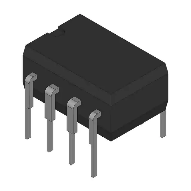
D OR P PACKAGE
(TOP VIEW)
Low Input Bias Current, 50 pA Typ
Low Input Noise Current, 0.01 pA/√Hz Typ
Low Supply Current, 2 mA Typ
High Input impedance, 1012 Ω Typ
Low Total Harmonic Distortion
Low 1/f Noise Corner, 50 Hz Typ
Package Options Include Plastic
Small-Outline (D) and Standard (P) DIPs
BAL1
IN –
IN +
VCC –
1
8
2
7
3
6
4
5
NC
VCC +
OUT
BAL2
NC – No internal connection
description
This device is a low-cost, high-speed, JFET-input operational amplifier with very low input offset voltage and
a maximum input offset voltage drift. It requires low supply current, yet maintains a large gain-bandwidth product
and a fast slew rate. In addition, the matched high-voltage JFET input provides very low input bias and offset
currents.
The LF411 can be used in applications such as high-speed integrators, digital-to-analog converters,
sample-and-hold circuits, and many other circuits.
The LF411C is characterized for operation from 0°C to 70°C. The LF411I is characterized for operation from
–40°C to 85°C.
symbol
IN –
IN +
BAL1
BAL2
2
–
3
6
OUT
+
1
5
AVAILABLE OPTIONS
TA
VIOmax
AT 25°C
0°C to 70°C
–40°C to 85°C
PACKAGE
SMALL OUTLINE
(D)
PLASTIC DIP
(P)
2 mV
LF411CD
LF411CP
2 mV
LF411ID
LF411IP
The D packages are available taped and reeled. Add the suffix R to the
device type (i.e., LF411CDR).
Please be aware that an important notice concerning availability, standard warranty, and use in critical applications of
Texas Instruments semiconductor products and disclaimers thereto appears at the end of this data sheet.
Copyright 1997, Texas Instruments Incorporated
PRODUCTION DATA information is current as of publication date.
Products conform to specifications per the terms of Texas Instruments
standard warranty. Production processing does not necessarily include
testing of all parameters.
POST OFFICE BOX 655303
• DALLAS, TEXAS 75265
1
�LF411
JFET-INPUT OPERATIONAL AMPLIFIER
SLOS011C – MARCH 1987 – REVISED OCTOBER 1997
absolute maximum ratings over operating free-air temperature range (unless otherwise noted)
Supply voltage, VCC + . . . . . . . . . . . . . . . . . . . . . . . . . . . . . . . . . . . . . . . . . . . . . . . . . . . . . . . . . . . . . . . . . . . . . . 18 V
Supply voltage, VCC – . . . . . . . . . . . . . . . . . . . . . . . . . . . . . . . . . . . . . . . . . . . . . . . . . . . . . . . . . . . . . . . . . . . . . – 18 V
Differential input voltage, VID . . . . . . . . . . . . . . . . . . . . . . . . . . . . . . . . . . . . . . . . . . . . . . . . . . . . . . . . . . . . . . . ± 30 V
Input voltage, VI (see Note 1) . . . . . . . . . . . . . . . . . . . . . . . . . . . . . . . . . . . . . . . . . . . . . . . . . . . . . . . . . . . . . . . ± 15 V
Duration of output short circuit . . . . . . . . . . . . . . . . . . . . . . . . . . . . . . . . . . . . . . . . . . . . . . . . . . . . . . . . . . . Unlimited
Continuous total power dissipation . . . . . . . . . . . . . . . . . . . . . . . . . . . . . . . . . . . . . . . . . . . . . . . . . . . . . . . . 500 mW
Package thermal impedance, θJA (see Note 2): D package . . . . . . . . . . . . . . . . . . . . . . . . . . . . . . . . . . 197°C/W
P package . . . . . . . . . . . . . . . . . . . . . . . . . . . . . . . . . . 104°C/W
Storage temperature range, Tstg . . . . . . . . . . . . . . . . . . . . . . . . . . . . . . . . . . . . . . . . . . . . . . . . . . . – 65°C to 150°C
Lead temperature 1,6 mm (1/16 inch) from case for 10 seconds . . . . . . . . . . . . . . . . . . . . . . . . . . . . . . . 260°C
NOTES: 1. Unless otherwise specified, the absolute maximum negative input voltage is equal to the negative power supply voltage.
2. The package thermal impedance is calculated in accordance with JESD 51, except for through-hole packages, which use a trace
length of zero.
recommended operating conditions
C SUFFIX
I SUFFIX
MIN
MIN
MAX
MAX
UNIT
Supply voltage, VCC +
3.5
18
3.5
18
V
Supply voltage, VCC –
– 3.5
– 18
– 3.5
– 18
V
0
70
– 40
–85
°C
Operating free-air temperature, TA
electrical characteristics over operating free-air temperature range, VCC ± = ±15 V (unless otherwise
specified)
PARAMETER
TA
TEST CONDITIONS
VIO
Input offset voltage
VIC = 0,
RS = 10 kΩ
αVIO
Average temperature coefficient of input offset voltage
VIC = 0,
RS = 10 kΩ
IIO
Inp t offset current
Input
c rrent‡
VIC = 0
IIB
Inp t bias current
Input
c rrent‡
VIC = 0
LF411C
LF411I
25°C
25°C
25°C
25°C
70°C
85°C
25°C
25°C
70°C
85°C
MIN
TYP
MAX
0.8
2
10
20†
µV/°C
25
100
pA
2
nA
200
pA
4
nA
50
UNIT
mV
± 11
–11.5
to
14.5
V
± 12
± 13.5
V
VICR
Common-mode input voltage
range
VOM
Maximum peak output-voltage
swing
RL = 10 kΩ
AVD
Large-signal
g
g
differential
voltage
VO = ± 10 V
V,
ri
Input resistance
TJ = 25°C
CMR
R
Common-mode rejection ratio
RS ≤ 10 kΩ
70
100
dB
kSVR
Supply-voltage rejection ratio
See Note 3
70
100
dB
RL = 2 kΩ
25°C
25°C
25
200
0°C to 70°C
–40°C to 85°C
15
200
1012
V/mV
Ω
ICC
Supply current
2
3.4
mA
† At least 90% of the devices meet this limit for αVIO.
‡ Input bias currents of an FET-input operational amplifier are normal junction reverse currents, which are temperature sensitive. Pulse techniques
must be used that will maintain the junction temperatures as close to the ambient temperature as possible.
NOTE 3: Supply-voltage rejection ratio is measured for both supply magnitudes increasing or decreasing simultaneously.
2
POST OFFICE BOX 655303
• DALLAS, TEXAS 75265
�LF411
JFET-INPUT OPERATIONAL AMPLIFIER
SLOS011C – MARCH 1987 – REVISED OCTOBER 1997
operating characteristics, VCC± = ±15 V, TA = 25°C
PARAMETER
TEST CONDITIONS
SR
Slew rate
B1
Vn
Unity-gain bandwidth
Equivalent input noise voltage
f = 1 kHz,
In
Equivalent input noise current
f = 1 kHz
MIN
TYP
8
13
2.7
POST OFFICE BOX 655303
RS = 20 Ω
• DALLAS, TEXAS 75265
MAX
UNIT
V/µs
3
MHz
18
nV/√Hz
0.01
pA/√Hz
3
�PACKAGE OPTION ADDENDUM
www.ti.com
6-Feb-2020
PACKAGING INFORMATION
Orderable Device
Status
(1)
Package Type Package Pins Package
Drawing
Qty
Eco Plan
Lead/Ball Finish
MSL Peak Temp
(2)
(6)
(3)
Op Temp (°C)
Device Marking
(4/5)
LF411CD
ACTIVE
SOIC
D
8
75
Green (RoHS
& no Sb/Br)
NIPDAU
Level-1-260C-UNLIM
0 to 70
LF411C
LF411CDR
ACTIVE
SOIC
D
8
2500
Green (RoHS
& no Sb/Br)
NIPDAU
Level-1-260C-UNLIM
0 to 70
LF411C
LF411CDRG4
ACTIVE
SOIC
D
8
2500
Green (RoHS
& no Sb/Br)
NIPDAU
Level-1-260C-UNLIM
0 to 70
LF411C
LF411CP
ACTIVE
PDIP
P
8
50
Green (RoHS
& no Sb/Br)
NIPDAU
N / A for Pkg Type
0 to 70
LF411CP
LF411CPE4
ACTIVE
PDIP
P
8
50
Green (RoHS
& no Sb/Br)
NIPDAU
N / A for Pkg Type
0 to 70
LF411CP
(1)
The marketing status values are defined as follows:
ACTIVE: Product device recommended for new designs.
LIFEBUY: TI has announced that the device will be discontinued, and a lifetime-buy period is in effect.
NRND: Not recommended for new designs. Device is in production to support existing customers, but TI does not recommend using this part in a new design.
PREVIEW: Device has been announced but is not in production. Samples may or may not be available.
OBSOLETE: TI has discontinued the production of the device.
(2)
RoHS: TI defines "RoHS" to mean semiconductor products that are compliant with the current EU RoHS requirements for all 10 RoHS substances, including the requirement that RoHS substance
do not exceed 0.1% by weight in homogeneous materials. Where designed to be soldered at high temperatures, "RoHS" products are suitable for use in specified lead-free processes. TI may
reference these types of products as "Pb-Free".
RoHS Exempt: TI defines "RoHS Exempt" to mean products that contain lead but are compliant with EU RoHS pursuant to a specific EU RoHS exemption.
Green: TI defines "Green" to mean the content of Chlorine (Cl) and Bromine (Br) based flame retardants meet JS709B low halogen requirements of
很抱歉,暂时无法提供与“LF411CP”相匹配的价格&库存,您可以联系我们找货
免费人工找货- 国内价格
- 5+13.70878
- 15+13.29223
- 75+12.76112