Product
Folder
Order
Now
Technical
Documents
Support &
Community
Tools &
Software
LM442-MIL
SNOSD59 – JUNE 2017
LF442-MIL Dual Low Power JFET Input Operational Amplifier
1 Features
3 Description
•
•
•
•
•
•
•
•
•
•
The LF442-MIL dual low power operational amplifiers
provide many of the same AC characteristics as the
industry standard LM1458 while greatly improving the
DC characteristics of the LM1458. The amplifiers
have the same bandwidth, slew rate, and gain (10 kΩ
load) as the LM1458 and only draw one tenth the
supply current of the LM1458. In addition the well
matched high voltage JFET input devices of the
LF442-MIL reduce the input bias and offset currents
by a factor of 10,000 over the LM1458. A combination
of careful layout design and internal trimming ensures
very low input offset voltage and voltage drift. The
LF442-MIL also has a very low equivalent input noise
voltage for a low power amplifier.
1
1/10 Supply Current of a LM1458: 400 μA (Max)
Low Input Bias Current: 50 pA (Max)
Low Input Offset Voltage: 1 mV (Max)
Low Input Offset Voltage Drift: 7 μV/°C (Typ)
High Gain Bandwidth: 1 MHz
High Slew Rate: 1 V/μs
Low Noise Voltage for Low Power: 35 nV/√Hz
Low Input Noise Current: 0.01 pA/√Hz
High Input Impedance: 1012Ω
High Gain VO = ±10V, RL = 10k: 50k (Min)
2 Applications
•
•
•
High Speed Integrators
Fast D/A Converters
Sample and Hold Circuits
The LF442-MIL is pin compatible with the LM1458
allowing an immediate 10 times reduction in power
drain in many applications. The LF442-MIL should be
used where low power dissipation and good electrical
characteristics are the major considerations.
Device Information(1)
PART NUMBER
PACKAGE
BODY SIZE (NOM)
LF442-MILACN
PDIP (8)
9.59 mm × 6.35 mm
LF442-MILAMH
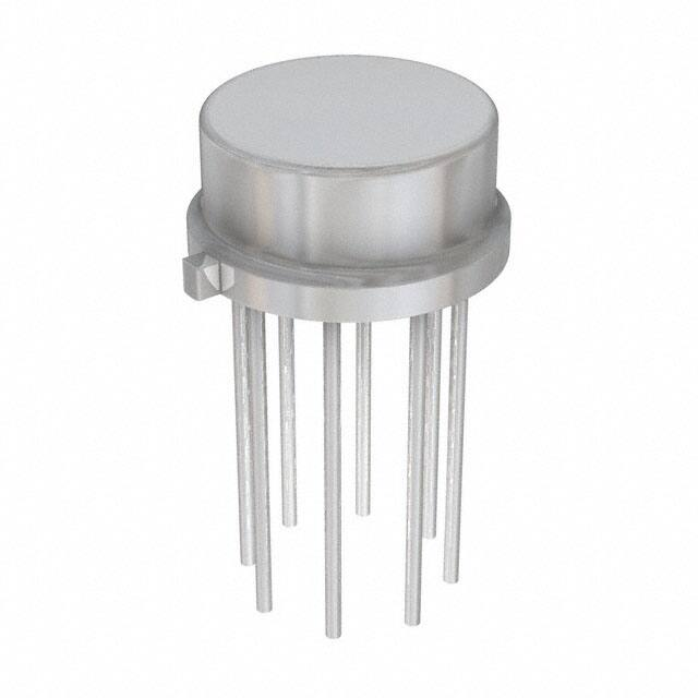
TO-99 (8)
8.96 mm Diameter
(1) For all available packages, see the orderable addendum at
the end of the data sheet.
Inverting Amplifier
Rf
VCC
Ri
±
+
LF442-MIL
-VEE
Copyright © 2017, Texas Instruments Incorporated
1
An IMPORTANT NOTICE at the end of this data sheet addresses availability, warranty, changes, use in safety-critical applications,
intellectual property matters and other important disclaimers. PRODUCTION DATA.
�LM442-MIL
SNOSD59 – JUNE 2017
www.ti.com
Table of Contents
1
2
3
4
5
6
7
Features ..................................................................
Applications ...........................................................
Description .............................................................
Revision History.....................................................
Pin Configuration and Functions .........................
Specifications.........................................................
1
1
1
2
3
4
6.1
6.2
6.3
6.4
6.5
6.6
6.7
4
4
4
4
5
5
6
Absolute Maximum Ratings ......................................
Absolute Maximum Ratings ......................................
Recommended Operating Conditions.......................
Thermal Information .................................................
DC Electrical Characteristics ....................................
AC Electrical Characteristics.....................................
Typical Characteristics ..............................................
7.3 Feature Description................................................. 11
7.4 Device Functional Modes........................................ 12
8
Application and Implementation ........................ 13
8.1 Application Information............................................ 13
8.2 Typical Applications ............................................... 13
9 Power Supply Recommendations...................... 19
10 Layout................................................................... 19
10.1 Layout Guidelines ................................................. 19
10.2 Layout Example .................................................... 19
11 Device and Documentation Support ................. 20
11.1
11.2
11.3
11.4
11.5
Detailed Description ............................................ 11
7.1 Overview ................................................................. 11
7.2 Functional Block Diagram ....................................... 11
Receiving Notification of Documentation Updates
Community Resources..........................................
Trademarks ...........................................................
Electrostatic Discharge Caution ............................
Glossary ................................................................
20
20
20
20
20
12 Mechanical, Packaging, and Orderable
Information ........................................................... 21
4 Revision History
NOTE: Page numbers for previous revisions may differ from page numbers in the current version.
2
DATE
REVISION
NOTES
June 2017
*
Initial release.
Submit Documentation Feedback
Copyright © 2017, Texas Instruments Incorporated
Product Folder Links: LM442-MIL
�LM442-MIL
www.ti.com
SNOSD59 – JUNE 2017
5 Pin Configuration and Functions
TO Package
8-Pin LMC
Top View
Pin 4 connected to case
P Package
8-Pin PDIP
Top View
Pin Functions
PIN
NAME
NO.
I/O
DESCRIPTION
Inverting input A
2
Input
Amplifier A inverting input
Inverting input B
6
Input
Amplifier B inverting input
Noninverting
input A
3
Input
Amplifier A noninverting input
Noninverting
input B
5
Input
Amplifier B noninverting Input
Output A
1
Output
Amplifier A output
Output B
7
Output
Amplifier B output
V+
8
Power
Positive supply
V-
4
Power
Negative supply
Submit Documentation Feedback
Copyright © 2017, Texas Instruments Incorporated
Product Folder Links: LM442-MIL
3
�LM442-MIL
SNOSD59 – JUNE 2017
www.ti.com
6 Specifications
6.1 Absolute Maximum Ratings (1) (2)
Supply voltage
±18 V
Differential input voltage
±30 V
Input voltage range (3)
±15 V
Output short circuit duration (4)
Continuous
Storage temperature, Tstg
(1)
(2)
(3)
(4)
–65 to 150°C
Stresses beyond those listed under Absolute Maximum Ratings may cause permanent damage to the device. These are stress ratings
only, which do not imply functional operation of the device at these or any other conditions beyond those indicated under Recommended
Operating Conditions. Exposure to absolute-maximum-rated conditions for extended periods may affect device reliability.
Refer to RETS442X for LF442MH military specifications.
Unless otherwise specified the absolute maximum negative input voltage is equal to the negative power supply voltage.
Any of the amplifier outputs can be shorted to ground indefinitely, however, more than one should not be simultaneously shorted as the
maximum junction temperature will be exceeded.
6.2 Absolute Maximum Ratings (1) (2)
LMC0008C Package
TJ max
150°C
Lead Temperature
(2)
(3)
(4)
115°C
See (3) (4)
Operating temperature range
(1)
P0008E Package
(Soldering, 10 sec.)
See (3) (4)
260°C
260°C
Stresses beyond those listed under Absolute Maximum Ratings may cause permanent damage to the device. These are stress ratings
only, which do not imply functional operation of the device at these or any other conditions beyond those indicated under Recommended
Operating Conditions. Exposure to absolute-maximum-rated conditions for extended periods may affect device reliability.
Refer to RETS442X for LF442MH military specifications.
These devices are available in both the commercial temperature range 0°C ≤ TA ≤ 70°C and the military temperature range −55°C ≤ TA
≤ 125°C. The temperature range is designated by the position just before the package type in the device number. A “C” indicates the
commercial temperature range and an “M” indicates the military temperature range. The military temperature range is available in “H”
package only.
The value given is in static air.
6.3 Recommended Operating Conditions
over operating free-air temperature range (unless otherwise noted)
MIN
NOM
MAX
UNIT
±15
V
Supply voltage
6.4 Thermal Information
LF442-MIL
THERMAL METRIC
RθJA
(Typical)
Junction-to-ambient thermal resistance
RθJC
(Typical)
Junction-to-case thermal resistance
(1)
4
(1)
LMC (TO)
P (PDIP)
8 PINS
8 PINS
400 linear feet/min air flow
65
114
Static air
165
152
21
UNIT
°C/W
°C/W
For more information about traditional and new thermal metrics, see the Semiconductor and IC Package Thermal Metrics application
report.
Submit Documentation Feedback
Copyright © 2017, Texas Instruments Incorporated
Product Folder Links: LM442-MIL
�LM442-MIL
www.ti.com
SNOSD59 – JUNE 2017
6.5 DC Electrical Characteristics (1) (2)
PARAMETER
TEST CONDITIONS
MIN
RS = 10 kΩ, TA = 25°C
VOS
Input offset voltage
ΔVOS/ΔT
Average TC of input offset
voltage
RS = 10 kΩ
IOS
Input offset voltage
VS = ±15 V (1) (3)
TYP
MAX
1
5
mV
7.5
mV
Over temperature
7
TJ = 25°C
5
TJ = 70°C
UNIT
μV/°C
50
pA
1.5
nA
TJ = 125°C
nA
TJ = 25°C
IB
Input bias current
VS = ±15 V (1) (3)
RIN
Input resistance
TJ = 25°C
AVOL
Large signal voltage gain
VS = ±15 V, VO = ±10 V,
RL = 10 kΩ, TA = 25°C
VO
Output voltage swing
10
TJ = 70°C
100
pA
3
nA
TJ = 125°C
Over temperature
VS = ±15 V, RL = 10 kΩ
nA
1012
Ω
25
200
V/mV
15
200
V/mV
±12
±13
V
±11
14
V
VCM
Input common-mode
voltage range
CMRR
Common-mode rejection ratio
RS ≤ 10 kΩ
70
PSRR
Supply voltage rejection ratio
See (4)
70
IS
Supply current
(1)
(2)
(3)
(4)
−12
V
95
dB
90
400
dB
500
μA
Unless otherwise specified, the specifications apply over the full temperature range of VS = ±15 V for the LF442-MIL. VOS, IB, and IOS
are measured at VCM = 0.
Refer to RETS442X for LF442-MIL MH military specifications.
The input bias currents are junction leakage currents which approximately double for every 10°C increase in the junction temperature,
TJ. Due to limited production test time, the input bias currents measured are correlated to junction temperature. In normal operation the
junction temperature rises above the ambient temperature as a result of internal power dissipation, PD. TJ = TA + θJAPD where θJA is the
thermal resistance from junction to ambient. Use of a heat sink is recommended if input bias current is to be kept to a minimum.
Supply voltage rejection ratio is measured for both supply magnitudes increasing or decreasing simultaneously in accordance with
common practice from ±15 V to ±5 V for the LF442-MIL.
6.6 AC Electrical Characteristics (1) (2)
PARAMETER
TEST CONDITIONS
MIN
TA = 25°C, f = 1 Hz-20 kHz (Input referred)
SR
Slew rate
VS = ±15 V, TA = 25°C
0.6
GBW
Gain-bandwidth product
VS = ±15 V, TA = 25°C
0.6
en
Equivalent input noise voltage
TA = 25°C, RS = 100 Ω, f = 1 kHz
in
Equivalent input noise current
TA = 25°C, f = 1 kHz
(1)
(2)
TYP
MAX
UNIT
−120
Amplifier to amplifier coupling
1
dB
V/μs
1
MHz
35
nV/√Hz
0.01
pA/√Hz
Unless otherwise specified, the specifications apply over the full temperature range and for VS = ±15 V for the LF442-MIL. VOS, IB, and
IOS are measured at VCM = 0.
Refer to RETS442X for LF442-MIL MH military specifications.
Submit Documentation Feedback
Copyright © 2017, Texas Instruments Incorporated
Product Folder Links: LM442-MIL
5
�LM442-MIL
SNOSD59 – JUNE 2017
www.ti.com
6.7 Typical Characteristics
6
Figure 1. Input Bias Current
Figure 2. Input Bias Current
Figure 3. Supply Current
Figure 4. Positive Common-Mode Input Voltage Limit
Figure 5. Negative Common-Mode Input Voltage Limit
Figure 6. Positive Current Limit
Submit Documentation Feedback
Copyright © 2017, Texas Instruments Incorporated
Product Folder Links: LM442-MIL
�LM442-MIL
www.ti.com
SNOSD59 – JUNE 2017
Typical Characteristics (continued)
Figure 7. Negative Current Limit
Figure 8. Output Voltage Swing
Figure 9. Output Voltage Swing
Figure 10. Gain Bandwidth
Figure 11. Bode Plot
Figure 12. Slew Rate
Submit Documentation Feedback
Copyright © 2017, Texas Instruments Incorporated
Product Folder Links: LM442-MIL
7
�LM442-MIL
SNOSD59 – JUNE 2017
www.ti.com
Typical Characteristics (continued)
8
Figure 13. Distortion vs Frequency
Figure 14. Undistorted Output Voltage Swing
Figure 15. Open Loop Frequency Response
Figure 16. Common-Mode Rejection Ratio
Figure 17. Power Supply Rejection Ratio
Figure 18. Equivalent Input Noise Voltage
Submit Documentation Feedback
Copyright © 2017, Texas Instruments Incorporated
Product Folder Links: LM442-MIL
�LM442-MIL
www.ti.com
SNOSD59 – JUNE 2017
Typical Characteristics (continued)
Figure 19. Open Loop Voltage Gain
Figure 20. Output Impedance
Figure 21. Inverter Settling Time
Submit Documentation Feedback
Copyright © 2017, Texas Instruments Incorporated
Product Folder Links: LM442-MIL
9
�LM442-MIL
SNOSD59 – JUNE 2017
www.ti.com
6.7.1 Pulse Response
RL = 10 kΩ, CL = 10 pF
Figure 22. Small Signal Inverting
Figure 23. Small Signal Non-Inverting
Figure 24. Large Signal Inverting
10
Submit Documentation Feedback
Figure 25. Large Signal Non-Inverting
Copyright © 2017, Texas Instruments Incorporated
Product Folder Links: LM442-MIL
�LM442-MIL
www.ti.com
SNOSD59 – JUNE 2017
7 Detailed Description
7.1 Overview
The LF442-MIL dual low power operational amplifiers provide many of the same AC characteristics as the
industry standard LM1458 while greatly improving the DC characteristics of the LM1458. The amplifiers have the
same bandwidth, slew rate, and gain (10 kΩ load) as the LM1458 and only draw one tenth the supply current of
the LM1458. In addition the well matched high voltage JFET input devices of the LF442-MIL reduce the input
bias and offset currents by a factor of 10,000 over the LM1458. A combination of careful layout design and
internal trimming ensures very low input offset voltage and voltage drift. The LF442-MIL also has a very low
equivalent input noise voltage for a low power amplifier.
The LF442-MIL is pin compatible with the LM1458 allowing an immediate 10 times reduction in power drain in
many applications. The LF442-MIL should be used where low power dissipation and good electrical
characteristics are the major considerations.
7.2 Functional Block Diagram
Figure 26. Each Amplifier
7.3 Feature Description
The amplifier's differential inputs consist of a non-inverting input (+IN) and an inverting input (-IN). The amplifier
amplifies only the difference in voltage between the two inputs, which is called the differential input voltage. The
output voltage of the op-amp VOUT is given by the equation VOUT = AOL(IN+ - IN-).
Submit Documentation Feedback
Copyright © 2017, Texas Instruments Incorporated
Product Folder Links: LM442-MIL
11
�LM442-MIL
SNOSD59 – JUNE 2017
www.ti.com
7.4 Device Functional Modes
7.4.1 Input and Output Stage
Figure 27. 1/2 Dual LF442-MIL
12
Submit Documentation Feedback
Copyright © 2017, Texas Instruments Incorporated
Product Folder Links: LM442-MIL
�LM442-MIL
www.ti.com
SNOSD59 – JUNE 2017
8 Application and Implementation
NOTE
Information in the following applications sections is not part of the TI component
specification, and TI does not warrant its accuracy or completeness. TI’s customers are
responsible for determining suitability of components for their purposes. Customers should
validate and test their design implementation to confirm system functionality.
8.1 Application Information
The LF442-MIL uses a combination of careful layout design and internal trimming to ensure very low input offset
voltage and voltage drift. The LF442-MIL also has a very low equivalent input noise voltage for a low power
amplifier. The LF442-MIL should be used where low power dissipation and good electrical characteristics are the
major considerations.
8.2 Typical Applications
1.
2.
3.
4.
5.
Battery Powered Strip Chart Preamplifier
"No FET" Low Power V to F Converter
High Efficiency Crystal Oven Controller
Conventional Log Amplifier
Unconvential Log Amplifier
8.2.1 Battery Powered Strip Chart Preamplifier
GAIN
INPUT
(+)
10 k
1
SEC
3+
5
SEC
10
SEC
50
SEC
100
SEC
½ LF442-MIL
1
2±
INPUT
(±)
1M
100 pF
1M
250 k
110 k
20.4 k
5M
10 M
50 M
100 M
10 k
9V
X1
X5
X10
X50
6
X100
GAIN
8
+
5 ±
1 F
7
½ LF442-MIL
OUTPUT TO
STRIP CHART
6
-9V
Copyright © 2017, Texas Instruments Incorporated
Figure 28. Battery Powered Strip Chart Preamplifier
8.2.1.1 Design Requirements
Runs from 9V batteries (±9V supplies).
Fully set gain and time constant.
Battery powered supply allows direct plug-in interface to strip chart recorder without common-mode problems.
Submit Documentation Feedback
Copyright © 2017, Texas Instruments Incorporated
Product Folder Links: LM442-MIL
13
�LM442-MIL
SNOSD59 – JUNE 2017
www.ti.com
Typical Applications (continued)
8.2.1.2 Detailed Design Procedure
This device is a dual low power op amp with internally trimmed input offset voltages and JFET input devices (BIFET II). These JFETs have large reverse breakdown voltages from gate to source and drain eliminating the need
for clamps across the inputs. Therefore, large differential input voltages can easily be accommodated without a
large increase in input current. The maximum differential input voltage is independent of the supply voltages.
However, neither of the input voltages should be allowed to exceed the negative supply as this will cause large
currents to flow which can result in a destroyed unit.
Exceeding the negative common-mode limit on either input will force the output to a high state, potentially
causing a reversal of phase to the output. Exceeding the negative common-mode limit on both inputs will force
the amplifier output to a high state. In neither case does a latch occur since raising the input back within the
common-mode range again puts the input stage and thus the amplifier in a normal operating mode.
Exceeding the positive common-mode limit on a single input will not change the phase of the output; however, if
both inputs exceed the limit, the output of the amplifier will be forced to a high state.
The amplifiers will operate with a common-mode input voltage equal to the positive supply; however, the gain
bandwidth and slew rate may be decreased in this condition. When the negative common-mode voltage swings
to within 3V of the negative supply, an increase in input offset voltage may occur.
Each amplifier is individually biased to allow normal circuit operation with power supplies of ±3.0V. Supply
voltages less than these may degrade the common-mode rejection and restrict the output voltage swing.
The amplifiers will drive a 10 kΩ load resistance to ± 10V over the full temperature range.
Precautions should be taken to ensure that the power supply for the integrated circuit never becomes reversed in
polarity or that the unit is not inadvertently installed backwards in a socket as an unlimited current surge through
the resulting forward diode within the IC could cause fusing of the internal conductors and result in a destroyed
unit.
A feedback pole is created when the feedback around any amplifier is resistive. The parallel resistance and
capacitance from the input of the device (usually the inverting input) to AC ground set the frequency of the pole.
In many instances the frequency of this pole is much greater than the expected 3 dB frequency of the closed
loop gain and consequently there is negligible effect on stability margin. However, if the feedback pole is less
than approximately 6 times the expected 3 dB frequency a lead capacitor should be placed from the output to the
input of the op amp. The value of the added capacitor should be such that the RC time constant of this capacitor
and the resistance it parallels is greater than or equal to the original feedback pole time constant.
8.2.1.3 Application Curves
2
Input
Output
1.5
Input/Output (V)
1
0.5
0
-0.5
-1
-1.5
-2
0
2
4
6
8
10
12
14
Time (s)
16
18
D001
Figure 29. Input and Output Waveforms, Gain = 10, Time Constant = 1 Second
14
Submit Documentation Feedback
Copyright © 2017, Texas Instruments Incorporated
Product Folder Links: LM442-MIL
�LM442-MIL
www.ti.com
SNOSD59 – JUNE 2017
Typical Applications (continued)
8.2.2 "No FET" Low Power V to F Converter
D3
10 K
D2
0.01
2 pF
15 V
1M
INPUT
0V to 10 V
2
3
1M
+
±
1M
1
½ LF442-MIL LM185
1.2 V
1M
5
6
+
±
-15 V
D1
7
OUTPUT
1 Hz to 1kHz
½ LF442-MIL
1M
-15 V
15 V
Copyright © 2017, Texas Instruments Incorporated
Figure 30. "No FET" Low Power V to F Converter
8.2.2.1 Design Requirements
1. Trim 1M pot for 1 kHz full-scale output.
2. 15 mW power drain.
3. No integrator reset FET required.
4. Mount D1 and D2 in close proximity.
5. 1% linearity to 1 kHz.
8.2.2.2 Detailed Design Procedure
See Section 8.2.1.2.
8.2.2.3 Application Curves
15
12
9
Input/Output (V)
6
3
0
-3
-6
-9
-12
Input
Output
-15
0
0.001
0.002
0.003
0.004
0.005
0.006
Time (s)
0.007
0.008
0.009
D001
Figure 31. Input and Output Waveforms
Submit Documentation Feedback
Copyright © 2017, Texas Instruments Incorporated
Product Folder Links: LM442-MIL
15
�LM442-MIL
SNOSD59 – JUNE 2017
www.ti.com
Typical Applications (continued)
8.2.3 High Efficiency Crystal Oven Controller
15 V
15 V
1.2 M
100 k
1N4148
1.2 M
20 k
TEMP TRIM
15 V
LM185-1.2
390 k*
2
1.2 M*
+
8 ½ LF442-MIL
1
3 ±
100 k
6
4
5
10 k
+
-15 V
R
LM395
±
0.1
15 V
½ LF442-MIL
7
100 k
1k
LM135
TEMP
SENSOR
1k
THERMAL FEEDBACK
Copyright © 2017, Texas Instruments Incorporated
Figure 32. High Efficiency Crystal Oven Controller
8.2.3.1 Design Requirements
1. Tcontrol= 75°C
2. A1's output represents the amplified difference between the LM335 temperature sensor and the crystal
oven's temperature.
3. A2, a free running duty cycle modulator, drives the LM395 to complete a servo loop.
4. Switched mode operation yields high efficiency.
5. 1% metal film resistor.
8.2.3.2 Detailed Design Procedure
See Section 8.2.1.2.
8.2.4 Conventional Log Amplifier
5k
100 k
15 V
120 k*
LM185-1.2
LM394
300 pF
2k
100 pF
±
RIN
EIN
100 k OFFSET
VOLTAGE ADJUST
RIN
2
3
±
½ LF442-MIL
1
15.7 k*
½ LF442-MIL
+
15 V
6
5
+
1M
T 1k
1k
-15 V
EOUT
Copyright © 2017, Texas Instruments Incorporated
Figure 33. Conventional Log Amplifier
16
Submit Documentation Feedback
Copyright © 2017, Texas Instruments Incorporated
Product Folder Links: LM442-MIL
�LM442-MIL
www.ti.com
SNOSD59 – JUNE 2017
Typical Applications (continued)
8.2.4.1 Design Requirements
1. RT = Tel Labs type Q81.
2. Trim 5k for 10 μA through the 5k–120k combination.
3. *1% film resistor
8.2.4.2 Detailed Design Procedure
See Section 8.2.1.2.
8.2.5 Unconventional Log Amplifier
15 V
12 V
LM340L-12
1k
10 k
Q1
10k*
LM329
100 k
SCALE
FACTOR
75 k* ADJUST
8
7
11
4
5 ± 12
21 2k
16 +
½ LF442-MIL
6
10
Q2
9
15 V
1N914
2.2 k*
17
1k
2N2907
±
27
8
7
+
½ LF442-MIL
OUTPUT
0 TO 10 V FOR
INPUTS OF 10 nA
-15 V
to 1 mA
2 k*
14
300 pF
13
Q3
15
10 k
1.4 k
12 V
2
I LOG INPUT
3
E LOG INPUT
15 V
±
+
1
½ LF442-MIL
10 M
50 k
ZERO
ADJUST
- 15 V
Copyright © 2017, Texas Instruments Incorporated
Figure 34. Unconventional Log Amplifier
8.2.5.1 Design Requirements
1. Q1, Q2, Q3 are included on LM389 amplifier chip which is temperature-stabilized by the LM389 and Q2-Q3,
which act as a heater-sensor pair.
2. Q1, the logging transistor, is thus immune to ambient temperature variation and requires no temperature
compensation at all.
Submit Documentation Feedback
Copyright © 2017, Texas Instruments Incorporated
Product Folder Links: LM442-MIL
17
�LM442-MIL
SNOSD59 – JUNE 2017
www.ti.com
Typical Applications (continued)
8.2.5.2 Detailed Design Procedure
See Section 8.2.1.2.
18
Submit Documentation Feedback
Copyright © 2017, Texas Instruments Incorporated
Product Folder Links: LM442-MIL
�LM442-MIL
www.ti.com
SNOSD59 – JUNE 2017
9 Power Supply Recommendations
For proper operation, the power supplies must be properly decoupled. For decoupling the supply lines it is
suggested that 0.1µF capacitors be placed as close as possible to the op amp power supply pins. The minimum
power supply voltage is ±5V.
10 Layout
10.1 Layout Guidelines
As with most amplifiers, care should be taken with lead dress, component placement and supply decoupling in
order to ensure stability. For example, resistors from the output to an input should be placed with the body close
to the input to minimize “pick-up” and maximize the frequency of the feedback pole by minimizing the
capacitance from the input to ground.
10.2 Layout Example
Figure 35. LF442-MIL Layout
Submit Documentation Feedback
Copyright © 2017, Texas Instruments Incorporated
Product Folder Links: LM442-MIL
19
�LM442-MIL
SNOSD59 – JUNE 2017
www.ti.com
11 Device and Documentation Support
11.1 Receiving Notification of Documentation Updates
To receive notification of documentation updates, navigate to the device product folder on ti.com. In the upper
right corner, click on Alert me to register and receive a weekly digest of any product information that has
changed. For change details, review the revision history included in any revised document.
11.2 Community Resources
The following links connect to TI community resources. Linked contents are provided "AS IS" by the respective
contributors. They do not constitute TI specifications and do not necessarily reflect TI's views; see TI's Terms of
Use.
TI E2E™ Online Community TI's Engineer-to-Engineer (E2E) Community. Created to foster collaboration
among engineers. At e2e.ti.com, you can ask questions, share knowledge, explore ideas and help
solve problems with fellow engineers.
Design Support TI's Design Support Quickly find helpful E2E forums along with design support tools and
contact information for technical support.
11.3 Trademarks
E2E is a trademark of Texas Instruments.
All other trademarks are the property of their respective owners.
11.4 Electrostatic Discharge Caution
This integrated circuit can be damaged by ESD. Texas Instruments recommends that all integrated circuits be handled with
appropriate precautions. Failure to observe proper handling and installation procedures can cause damage.
ESD damage can range from subtle performance degradation to complete device failure. Precision integrated circuits may be more
susceptible to damage because very small parametric changes could cause the device not to meet its published specifications.
11.5 Glossary
SLYZ022 — TI Glossary.
This glossary lists and explains terms, acronyms, and definitions.
20
Submit Documentation Feedback
Copyright © 2017, Texas Instruments Incorporated
Product Folder Links: LM442-MIL
�LM442-MIL
www.ti.com
SNOSD59 – JUNE 2017
12 Mechanical, Packaging, and Orderable Information
The following pages include mechanical, packaging, and orderable information. This information is the most
current data available for the designated devices. This data is subject to change without notice and revision of
this document. For browser-based versions of this data sheet, refer to the left-hand navigation.
Submit Documentation Feedback
Copyright © 2017, Texas Instruments Incorporated
Product Folder Links: LM442-MIL
21
�PACKAGE OPTION ADDENDUM
www.ti.com
20-May-2025
PACKAGING INFORMATION
Orderable part number
(1)
Status
Material type
(1)
(2)
Package | Pins
Package qty | Carrier
RoHS
(3)
Lead finish/
Ball material
MSL rating/
Peak reflow
(4)
(5)
Op temp (°C)
Part marking
(6)
LF442-MWA
Active
Production
WAFERSALE (YS) | 0
1 | NOT REQUIRED
-
Call TI
Level-1-NA-UNLIM
-40 to 85
LF442AMH
Active
Production
TO-99 (LMC) | 8
500 | TRAY NON-STD
No
Call TI
Level-1-NA-UNLIM
-55 to 125
( LF442AMH, LF442A
MH)
LF442AMH/NOPB
Active
Production
TO-99 (LMC) | 8
500 | OTHER
Yes
Call TI
Level-1-NA-UNLIM
-55 to 125
( LF442AMH, LF442A
MH)
Status: For more details on status, see our product life cycle.
(2)
Material type: When designated, preproduction parts are prototypes/experimental devices, and are not yet approved or released for full production. Testing and final process, including without limitation quality assurance,
reliability performance testing, and/or process qualification, may not yet be complete, and this item is subject to further changes or possible discontinuation. If available for ordering, purchases will be subject to an additional
waiver at checkout, and are intended for early internal evaluation purposes only. These items are sold without warranties of any kind.
(3)
RoHS values: Yes, No, RoHS Exempt. See the TI RoHS Statement for additional information and value definition.
(4)
Lead finish/Ball material: Parts may have multiple material finish options. Finish options are separated by a vertical ruled line. Lead finish/Ball material values may wrap to two lines if the finish value exceeds the maximum
column width.
(5)
MSL rating/Peak reflow: The moisture sensitivity level ratings and peak solder (reflow) temperatures. In the event that a part has multiple moisture sensitivity ratings, only the lowest level per JEDEC standards is shown.
Refer to the shipping label for the actual reflow temperature that will be used to mount the part to the printed circuit board.
(6)
Part marking: There may be an additional marking, which relates to the logo, the lot trace code information, or the environmental category of the part.
Multiple part markings will be inside parentheses. Only one part marking contained in parentheses and separated by a "~" will appear on a part. If a line is indented then it is a continuation of the previous line and the two
combined represent the entire part marking for that device.
Important Information and Disclaimer:The information provided on this page represents TI's knowledge and belief as of the date that it is provided. TI bases its knowledge and belief on information provided by third parties, and
makes no representation or warranty as to the accuracy of such information. Efforts are underway to better integrate information from third parties. TI has taken and continues to take reasonable steps to provide representative
and accurate information but may not have conducted destructive testing or chemical analysis on incoming materials and chemicals. TI and TI suppliers consider certain information to be proprietary, and thus CAS numbers
and other limited information may not be available for release.
In no event shall TI's liability arising out of such information exceed the total purchase price of the TI part(s) at issue in this document sold by TI to Customer on an annual basis.
Addendum-Page 1
�PACKAGE OUTLINE
LMC0008A
TO-CAN - 5.72 mm max height
TRANSISTOR OUTLINE
.305-.335
[7.75-8.51]
.165-.185
[4.19-4.70]
.040 MAX
[1.02]
.225
MAX
[5.72]
C
.010-.040
[0.25-1.02]
UNCONTROLLED
LEAD DIA
.055[1.397] MAX
SEATING PLANE
.500 MIN
[12.7]
8X
.016-.021
[0.41-0.53]
.010 [0.25]
C A
.110-.160
[2.79-4.06]
.100
[2.54]
4
5
.335-.370
[8.51-9.40]
3
6
.200
[5.08]
2
A
7
1
8
45 TYP
.029-.045
[0.74-1.14]
.028-.034
[0.71-0.86]
4220610/B 09/2024
NOTES:
1. All linear dimensions are in inches [millimeters]. Any dimensions in parenthesis are for reference only. Dimensioning and tolerancing
per ASME Y14.5M.
2. This drawing is subject to change without notice.
3. Pin numbers shown for reference only. Numbers may not be marked on package.
4. Reference JEDEC registration MO-002/TO-99.
www.ti.com
�EXAMPLE BOARD LAYOUT
LMC0008A
TO-CAN - 5.72 mm max height
TRANSISTOR OUTLINE
METAL
( .055)
[1.4]
8
8X ( .031) VIA
[0.8]
7X ( .055)
[1.4]
METAL
7
1
.003 MAX
[0.07]
ALL AROUND
(R.002 ) TYP
[0.05]
7X SOLDER MASK
OPENING
SOLDER MASK
OPENING
6
2
7X .003 MAX
[0.07]
ALL AROUND
(45 ) TYP
5
3
( .200 )
[5.08]
4
LAND PATTERN EXAMPLE
NON-SOLDER MASK DEFINED
SCALE: 12X
4220610/B 09/2024
www.ti.com
�IMPORTANT NOTICE AND DISCLAIMER
TI PROVIDES TECHNICAL AND RELIABILITY DATA (INCLUDING DATA SHEETS), DESIGN RESOURCES (INCLUDING REFERENCE
DESIGNS), APPLICATION OR OTHER DESIGN ADVICE, WEB TOOLS, SAFETY INFORMATION, AND OTHER RESOURCES “AS IS”
AND WITH ALL FAULTS, AND DISCLAIMS ALL WARRANTIES, EXPRESS AND IMPLIED, INCLUDING WITHOUT LIMITATION ANY
IMPLIED WARRANTIES OF MERCHANTABILITY, FITNESS FOR A PARTICULAR PURPOSE OR NON-INFRINGEMENT OF THIRD
PARTY INTELLECTUAL PROPERTY RIGHTS.
These resources are intended for skilled developers designing with TI products. You are solely responsible for (1) selecting the appropriate
TI products for your application, (2) designing, validating and testing your application, and (3) ensuring your application meets applicable
standards, and any other safety, security, regulatory or other requirements.
These resources are subject to change without notice. TI grants you permission to use these resources only for development of an
application that uses the TI products described in the resource. Other reproduction and display of these resources is prohibited. No license
is granted to any other TI intellectual property right or to any third party intellectual property right. TI disclaims responsibility for, and you
will fully indemnify TI and its representatives against, any claims, damages, costs, losses, and liabilities arising out of your use of these
resources.
TI’s products are provided subject to TI’s Terms of Sale or other applicable terms available either on ti.com or provided in conjunction with
such TI products. TI’s provision of these resources does not expand or otherwise alter TI’s applicable warranties or warranty disclaimers for
TI products.
TI objects to and rejects any additional or different terms you may have proposed. IMPORTANT NOTICE
Mailing Address: Texas Instruments, Post Office Box 655303, Dallas, Texas 75265
Copyright © 2025, Texas Instruments Incorporated
�