Not Recommended For New Designs
LHV870
www.ti.com
SNOSB50B – MAY 2011 – REVISED MAY 2013
LHV870 44V Single High Performance, High Voltage Operational Amplifier
Check for Samples: LHV870
FEATURES
DESCRIPTION
•
•
•
The LHV870 is an ultra-low distortion, low noise, high
slew rate operational amplifier optimized and fully
specified for high performance, high voltage
applications. Combining advanced leading-edge
process technology with state-of-the-art circuit
design, the LHV870 operational amplifier delivers
superior signal amplification for outstanding
performance. The LHV870 combines extremely low
voltage noise density (2.7nV/√Hz) with vanishingly
low DC Gain Linearity Error (0.000009%) to easily
satisfy the most demanding applications. To ensure
that the most challenging loads are driven without
compromise, the LHV870 has a high slew rate of
±20V/μs and an output current capability of ±26mA.
Further, dynamic range is maximized by an output
stage that drives 2kΩ loads to within 1V of either
power supply voltage and to within 1.4V when driving
600Ω loads.
1
2
Easily Drives 600Ω Loads
Output Short Circuit Protection
PSRR and CMRR Exceed 120dB (Typ)
APPLICATIONS
•
•
•
•
•
•
Low Noise Industrial Applications Including
Test, Measurement, and Ultrasound
High Quality Audio Amplification
High Fidelity Preamplifiers, Phono Preamps,
and Multimedia
High Performance Professional Audio
High Fidelity Equalization and Crossover
Networks with Active Filters
High Performance Line Drivers and Receivers
KEY SPECIFICATIONS
•
•
•
•
•
•
•
•
•
Power Supply Voltage Range ±2.5V to ±22 V
Input Noise Density 2.7nV/√Hz (Typ)
Slew Rate ±20V/μs (Typ)
Gain Bandwidth Product 55 MHz (Typ)
Open Loop Gain (RL = 600Ω) 140 dB (Typ)
Input Bias Current 10nA (Typ)
Input Offset Voltage 0.1mV (Typ)
DC Gain Linearity Error 0.000009%
THD+N (AV = 1, VOUT = 3VRMS, fIN = 1kHz)
– RL = 2kΩ 0.00003% (Typ)
– RL = 600Ω 0.00003% (Typ)
100
The LHV870's outstanding CMRR (120dB), PSRR
(120dB), and VOS (0.1mV) give the amplifier excellent
DC performance.
The LHV870 operates over a wide supply range of
±2.5V to ±22V and is unity gain stable. This
operational amplifier achieves outstanding AC
performance while driving complex loads with values
as high as 100pF.
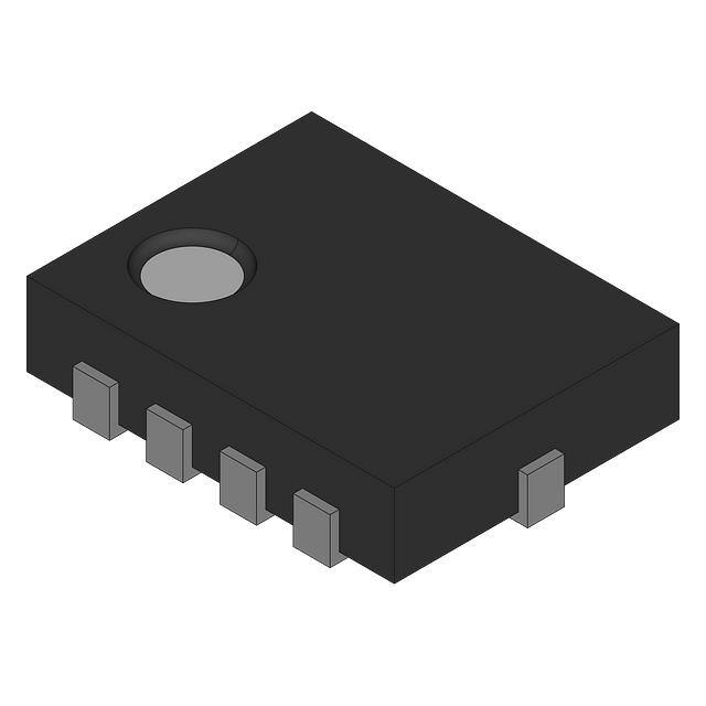
The LHV870 is available in 10-lead WQFN package.
100
180
VS = 30V
160
10
10
2.7 nV/Hz
GAIN (dB), PHASE LAG (°)
VOLTAGE NOISE (nV/Hz)
VCM = 15V
140
120
100
80
60
40
20
0
1
1
10
100
1000
1
10000 100000
FREQUENCY (Hz)
-20
10
100
1k
10k 100k
1M
10M 100M
FREQUENCY (Hz)
1
2
Please be aware that an important notice concerning availability, standard warranty, and use in critical applications of
Texas Instruments semiconductor products and disclaimers thereto appears at the end of this data sheet.
All trademarks are the property of their respective owners.
PRODUCTION DATA information is current as of publication date.
Products conform to specifications per the terms of the Texas
Instruments standard warranty. Production processing does not
necessarily include testing of all parameters.
Copyright © 2011–2013, Texas Instruments Incorporated
�Not Recommended For New Designs
LHV870
SNOSB50B – MAY 2011 – REVISED MAY 2013
www.ti.com
Connection Diagram
VCC
NC
1
NC
10
9
OUTPUT 1
2
8
NC
NC
3
7
IN-1
NC
4
6
IN+1
5
VEE/GND
Figure 1. See Package Number – NKY0010A
These devices have limited built-in ESD protection. The leads should be shorted together or the device placed in conductive foam
during storage or handling to prevent electrostatic damage to the MOS gates.
ABSOLUTE MAXIMUM RATINGS (1) (2) (3)
Power Supply Voltage (VS = V+ - V-)
46V
−65°C to 150°C
Storage Temperature
Input Voltage
(V-) - 0.7V to (V+) + 0.7V
Output Short Circuit (4)
Continuous
Power Dissipation
Internally Limited
ESD Rating (5)
ESD Rating (6)
2000V
Pins 1, 4, 7 and 8
200V
Pins 2, 3, 5 and 6
100V
Junction Temperature
Thermal Resistance
(1)
(2)
(3)
(4)
(5)
(6)
2
150°C
θJA (WQFN)
168°C/W
“Absolute Maximum Ratings” indicate limits beyond which damage to the device may occur, including inoperability and degradation of
device reliability and/or performance. Functional operation of the device and/or non-degradation at the Absolute Maximum Ratings or
other conditions beyond those indicated in the Recommended Operating Conditions is not implied. The Recommended Operating
Conditions indicate conditions at which the device is functional and the device should not be operated beyond such conditions. All
voltages are measured with respect to the ground pin, unless otherwise specified.
The Electrical Characteristics tables list ensured specifications under the listed Recommended Operating Conditions except as
otherwise modified or specified by the Electrical Characteristics Conditions and/or Notes. Typical specifications are estimations only and
are not ensured.
If Military/Aerospace specified devices are required, please contact the Texas Instruments Sales Office/Distributors for availability and
specifications.
The maximum power dissipation must be derated at elevated temperatures and is dictated by TJMAX, θJA, and the ambient temperature,
TA. The maximum allowable power dissipation is PDMAX = (TJMAX - TA) / θJA or the number given in Absolute Maximum Ratings,
whichever is lower.
Human body model, applicable std. JESD22-A114C.
Machine model, applicable std. JESD22-A115-A.
Submit Documentation Feedback
Copyright © 2011–2013, Texas Instruments Incorporated
Product Folder Links: LHV870
�Not Recommended For New Designs
www.ti.com
LHV870
SNOSB50B – MAY 2011 – REVISED MAY 2013
OPERATING RATINGS
Temperature Range (TMIN ≤ TA ≤ TMAX)
−40°C ≤ TA ≤ 85°C
Supply Voltage Range
±2.5V ≤ VS ≤ ±22V
ELECTRICAL CHARACTERISTICS FOR THE LHV870 (1)
The following specifications apply for VS = ±18V and ±22V, RL = 2kΩ, RSOURCE = 10Ω, fIN = 1kHz, TA = 25°C, unless otherwise
specified.
Symbol
THD+N
IMD
Parameter
Conditions
LHV870
Typical
(2)
Limit (3)
Units
(Limits)
Total Harmonic Distortion + Noise
AV = 1, VOUT = 3VRMS, RL = 2kΩ
0.00003
%
Intermodulation Distortion
AV = 1, VOUT = 3VRMS
Two-tone, 60Hz & 7kHz 4:1
0.00005
%
GBWP
Gain Bandwidth Product
55
SR
Slew Rate
±20
45
MHz (min)
V/μs
10
MHz
μs
FPBW
Full Power Bandwidth
VOUT = 1VP-P, –3dB
referenced to output magnitude
at f = 1kHz
ts
Settling time
AV = –1, 10V step, CL = 100pF
0.1% error range
1.2
Equivalent Input Noise Voltage
fBW = 20Hz to 20kHz
0.34
0.65
μVRMS
(max)
Equivalent Input Noise Density
f = 1kHz
2.5
4.7
nV/√Hz
(max)
Current Noise Density
f = 1kHz
en
in
VOS
Offset Voltage
ΔVOS/ΔTemp
Average Input Offset Voltage Drift
vs Temperature
1.6
VS = ±18V
±0.12
VS = ±22V
±0.14
–40°C ≤ TA ≤ 85°C
VS = ±18V, ΔVS = 24V
VS = ±22V, ΔVS = 30V
IB
Input Bias Current
ΔIOS/ΔTemp
Input Bias Current Drift
vs Temperature
IOS
Input Offset Current
VCM = 0V
11
VS = ±18V
+17.1
–16.9
VS = ±22V
+21.0
–20.8
VIN-CM
CMRR
ZIN
(1)
(2)
(3)
(4)
110
VCM = 0V
10
300
–40°C ≤ TA ≤ 85°C
0.2
dB (min)
nA (max)
nA/°C
100
nA (max)
V
V
(V+) – 2.0
(V-) + 2.0
V (min)
V (min)
VS = ±18V
–12V≤VCM≤12V
120
VS = ±22V
–15V≤VCM≤15V
120
30
kΩ
–10V