User's Guide
SNOU108A – December 2012 – Revised April 2013
LM10011 Evaluation Module
1
Introduction
This application report describes the various functions of the LM10011 evaluation module, how to test and
evaluate it, and how to use the GUI design tool to change the components for a specific application.
Please check the LM10011 GUI Installer (SNVC071) for the latest software and the 6/4-Bit VID
Programmable Current DAC for Point of Load Regulators with Adjustable Start-Up Current (SNVS822).
For more information on the LM21215A-1 and its operation, please check the LM21215A-1 15A High
Efficiency Synchronous Buck Regulator with Frequency Synchronization (SNOSB87) and the AN-2131
LM21215A-1 Evaluation Board User's Guide (SNVA477).
The LM10011 is a precision, digitally programmable device used to control the output voltage of a DC/DC
converter. The LM10011 outputs a DC current proportional to a 6-bit or 4-bit input word. The current DAC
output is intended to connect to the feedback node of a buck converter in order to adjust the converter
output voltage to a desired range and resolution. As the 6-bit or 4-bit word counts up, the output voltage is
adjusted higher based on the setting of the feedback resistors in the buck converter.
The LM10011 evaluation module provides the power design engineer with a low voltage high current
point-of-load solution with an adjustable output voltage using the LM10011 VID controlled current DAC, an
LM21215A-1 15A integrated buck regulator, and a companion GUI software. The GUI software along with
included hardware are used to assist in the design and understanding of how to implement the LM10011.
The GUI can be used to change the output voltage of the on-board POL based on direct user input. It is
also able to assist the power designer in selecting the correct external components needed for any given
application.
2
PCB Features
•
•
•
•
•
•
•
3
Input voltage range: 2.97V to 5.5V
VOUT at start-up: 0.9V
Programmable output voltage: 0.7V to 1.1V (adjustable)
Over current protection: 17A
PCB Size: 2.2” x 2.8”
USB connection through communications dongle
Software control with graphical user interface
Evaluation Module Introduction
The evaluation module provides a VID interface to test the LM10011 and its control of an LM21215A-1
buck regulator. The LM21215A-1 is capable of driving up to 15A of continuous load current with excellent
output voltage accuracy due to its ±1% internal voltage reference and high gain error amplifier. The
LM21215A-1 also features a clock synchronization input (SYNC), precision enable pin (ENABLE), a power
good output (PGOOD), and a soft-start and track pin (SS_TRK) (as labeled on the PCB). The input
voltage can be operated from 2.97V to 5.5V. On power-up, the output voltage defaults to 0.9V. The
evaluation board allows for control of the LM21215A-1 output voltage from 0.7V to 1.1V in 6.4mV steps
through the 4-pin VID interface of the LM10011. A 10-pin header is included to communicate with the
LM10011. A USB communications dongle is provided along with software to control the output voltage
through a graphical user interface (GUI) and a USB port.
SNOU108A – December 2012 – Revised April 2013
Submit Documentation Feedback
Copyright © 2012–2013, Texas Instruments Incorporated
LM10011 Evaluation Module
1
�Simplified Schematic
4
www.ti.com
Simplified Schematic
VOUT_MIN = 0.7V
V
= 1.1V
VOUT OUT_MAX
VOUT_START-UP = 0.9V
IOUT_MAX = 15A
VIN = 2.97V to 5.5V
VIN
PVIN
SW
RFB1
6.81kÖ
LM21215A-1
FB
GND 10
VIDC
8
3V3
6
4
GND 2
RFB2
8.06kÖ
FB
1
GND
2
1
2
R2 1Ö
2
3
REN
1 MÖ
3
CDD
1 uF
4
5
LM10011
GND
VIDS
IDAC_OUT
VIDC
VDD
VIDB
EN
VIDA
MODE
SET
VDD
DAP
PEN
VDD
VDD 4-Bit 1
2
GND 6-Bit 3
9
7
5
3
1
VIDS
VIDB
VIDA
IDAC
VIN
JP1
1
J1
10
R3 100Ö
9
R4 100Ö
8
R5 100Ö
7
R6 100Ö
6
RSET 118kÖ
R7 100Ö
JP2
Figure 1. Simplified Schematic
2
LM10011 Evaluation Module
SNOU108A – December 2012 – Revised April 2013
Submit Documentation Feedback
Copyright © 2012–2013, Texas Instruments Incorporated
�Theory of Operation
www.ti.com
5
Theory of Operation
The LM10011 can be thought of as a D/A converter, converting the VID codes to analog outputs. In this
device, the output is a current DAC (IDAC_OUT), which is connected to the feedback node of a slave
regulator. Therefore, all VID data words are decoded into a 6-bit current DAC output. The impedance of
the feedback node at DC appears as the top feedback resistor. This is because the control loop of the
slave regulator effectively maintains a constant current and voltage through and across the bottom
feedback resistor. Therefore, as more current is sourced into the feedback node, less current is needed
from RFB1 and the output voltage is reduced. See Figure 2.
Slave Regulator
VOUT
+
FB
+
RFB1
IRFB1
LM10011
IDAC_OUT
VRFB1
+-
-
VOUT
+
LM10011
RFB2
IRFB2
VID
-
VFB
-
IDAC_OUT
Figure 2. Current Injection into the Feedback Node
Looking at Figure 2, the following equation defines VOUT for a given regulator
(valid for VOUT > VFB, VFB = voltage at FB pin):
VOUT = VFB x 1+ RFB1 - IDAC_OUT x RFB1
RFB2
(1)
For the LM21215A-1, VFB is 600mV. For the LM10011, the IDAC_OUT maximum current is 59.2µA, with
64 settings at a resolution of 940nA, adjustable with the 6-bit VID word. Note that as the VID codes count
up, the output current (IDAC_OUT) counts down starting from the highest current. This allows for VOUT to
increment up with the VID code. For a more in-depth analysis of the circuit, see the LM10011 datasheet.
Table 1 shows the codes and some of the resultant values of IDAC_OUT current and corresponding
regulator output voltage for the default resistor values on the evaluation board.
Table 1. VID Codes with IDAC Current and Regulator Voltage for the Evaluation Board
VID Code
IDAC Current (µA)
Regulator Voltage (V)
000000b
59.2
0.704
000001b
58.3
0.710
000010b
57.4
0.716
000011b
56.4
0.723
:
:
:
111100b
2.87
1.087
111101b
1.93
1.094
111110b
1.00
1.100
111111b
0.06
1.107
SNOU108A – December 2012 – Revised April 2013
Submit Documentation Feedback
Copyright © 2012–2013, Texas Instruments Incorporated
LM10011 Evaluation Module
3
�Power-Up Procedures
6
www.ti.com
Power-Up Procedures
CAUTION
Read the entire power-up procedures prior to applying power to the evaluation
board.
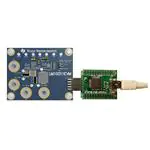
The LM10011 evaluation kit hardware is shown in Figure 3. The board offers a connection for the system
input voltage on the left side and a connection for the load on the bottom. To the right of the LM10011
evaluation module is a communications dongle. It is connected to the board through the 10 pin right angle
header and is used to communicate with the LM10011. A USB cable connects the dongle to a USB port
on the computer for software control.
Figure 3. LM10011 Evaluation Kit Hardware
6.1
Quick Setup Procedure
Step 1:Before connecting the input power supply, set the output of the power supply to current limit at 10A
and output voltage two any voltage between 2.97V and 5.5V. Disable the power supply output. Connect
the positive output (+) of the power supply to VIN and the negative output (-) to the corresponding GND.
Be sure to disable the output of the power supply before connecting it to the evaluation board.
Minimize the inductance between the power supply and the evaluation board to mitigate any
voltage spikes that may occur.
Step 2: Connect the load (with 15A capability) positive (+) input to VOUT and negative (-) input to the
corresponding GND on the evaluation board.
Step 3: The ENABLE pin should be left open for normal operation.
Step 4: Activate the output of the power supply. The load voltage should be in regulation with a nominal
0.9V output.
Step 5: Slowly increase the load while monitoring the load voltage at VOUT SENSE. It should remain in
regulation with a nominal 0.9V output as the load is increased up to 15A.
Step 6: Slowly sweep the input source voltage from 2.97V to 5.5V (DO NOT EXCEED 5.5V). The load
voltage should remain in regulation with a nominal 0.9V output. If desired, the output of the device can be
disabled by connecting the ENABLE pin to GND.
Step 7: The LM21215A-1 switching frequency can be varied by connecting a 2.0V clock signal between
SYNC and GND.
4
LM10011 Evaluation Module
SNOU108A – December 2012 – Revised April 2013
Submit Documentation Feedback
Copyright © 2012–2013, Texas Instruments Incorporated
�Connection Descriptions
www.ti.com
6.2
Over-Current Protection
The evaluation board is configured with over-current protection. This function is completely contained in
the LM21215A-1. The peak current is limited to approximately 17A.
6.3
Quick Setup for Software Control
Once the LM10011 evaluation board is setup and the LM21215A-1 is determined to be correctly regulating
the output voltage, the software can be installed and communication can then be established with the
LM10011. In the evaluation board kit, there should be a CD with all the necessary executable files to
install the LM10011 GUI. If there is no CD, the software can be found in the LM10011 GUI Installer
(SNVC071).
The installation files should be executed on a PC running Windows XP or later.
7
Connection Descriptions
Terminal Silkscreen
Description
VIN
This terminal is the input voltage to the evaluation board. The evaluation board will operate over the
input voltage range of 2.97V to 5.5V.
GND
These terminals are the ground connections to the device. The input power ground should be connected
next to the input VIN connection, and the output power ground next to the VOUT connection.
VOUT
This terminal connects to the output voltage of the power supply and should be connected to the load.
ENABLE
This terminal connects to the enable pin of the LM21215A-1. ENABLE can be left floating or driven
externally. If left floating, a 2 µA current source will pull the pin high, thereby enabling the device. If
driven externally, a voltage typically less than 1.24V will disable the LM21215A-1 and above 1.35V will
enable the LM21215A-1.
SS/TRK
This terminal provides access to the SS/TRK pin of the LM21215A-1. Connections to SS/TRK are not
needed for most applications. The feedback pin of the device will track the voltage on the SS/TRK pin if
it is driven with an external voltage source that is below the 0.6V reference.
PGOOD
This terminal connects to the power good output of the LM21215A-1. This pin is pulled up through a
10kΩ pull-up resistor to VIN.
AC INJ
This terminal block allows the user to insert an AC injection signal across a 49.9Ω resistor for open loop
gain bode measurements. A jumper shorts this resistor when it is not needed.
SWITCH
SYNC
VIN_SENSE+,
VIN_SENSE-,
VOUT_SENSE+,
VOUT_SENSE-
This terminal allows easy probing of the switch node. Do not apply any external voltage source to this
pin.
This terminal connects to the SYNC pin of the LM21215A-1. The regulator can synchronize the SWITCH
pin to a SYNC signal with a frequency between 300kHz and 1.5MHz. If this pin is left open, the switching
frequency will default to 500kHz.
These terminals allow a sense connection on the board for accurate VIN and VOUT measurements,
respectively.
IDAC
This terminal connects to the LM10011 IDAC output (IDAC_OUT).
PEN
This terminal connects to the enable (EN) pin of the LM10011. EN can be left floating or driven
externally. If left floating, a 2µA current source will pull the LM10011 EN pin high, thereby enabling the
LM10011. If driven externally, a voltage typically less than 1.24V will disable the LM10011 and above
1.34V will enable the LM10011.
FB
This jumper connects the LM10011 output to the feedback node of the LM21215A-1. If the LM10011 is
used to control the output voltage, then this jumper is required. If the LM10011 is to be evaluated alone,
then the IDAC_OUT current can be observed at the IDAC connection by removing the jumper.
J1
This terminal block is used to connect the LM10011 evaluation board with the communications dongle.
JP1
This terminal block controls the source of power for the LM10011. If a jumper is connected between pins
1 and 2, then the LM10011 supply comes from PVIN. If the jumper is connected from pins 2 and 3, then
the LM10011 derives power from an external connection to VDD.
JP2
This terminal block controls the mode of the LM10011. To put the LM10011 into 4-Bit mode, set the
terminal block to VDD. For 6-Bit mode, set the terminal block to GND.
VDD
This terminal can be used as an alternate power source for the LM10011 though terminal block JP1.
SNOU108A – December 2012 – Revised April 2013
Submit Documentation Feedback
Copyright © 2012–2013, Texas Instruments Incorporated
LM10011 Evaluation Module
5
�Evaluation Board
8
www.ti.com
Evaluation Board
The evaluation board shows how the LM10011 is used to control the LM21215A-1. However, the
LM10011 can operate independently without the LM21215A-1 by jumpering pins 2 and 3 on JP1 and
applying the supply voltage through the VDD test point. The IDAC_OUT output current can be observed at
the IDAC test point with the jumper removed from FB.
Additionally, the output voltage range of the evaluation board can be adjusted by replacing the RFB1 and
RFB2 feedback resistors on the board. However , a change in the feedback resistors may change the
compensation network for the LM21215A-1 and this may require adjustments in values for CC1, CC2, CC3,
RC1, and RC2. For further guidance with component selection, please see the LM21215A-1 datasheet and
evaluation board user's guide.
9
LM10011 Control and Design Software
The LM10011 evaluation board comes with a communications dongle and software to control the output
voltage (software can also be found on the LM10011 Texas Instruments Product Folder online). This
section describes software features and modes of operation. The software has a built-in calculator to
determine the feedback resistor values for a given range and resolution of operation. This is only used
when the user decides to remove the existing default resistor feedback values and determines the
LM21215A-1's compensation is correct for the new feedback resistors. The default or updated values are
used to calculate expected output voltages of the point of load regulator. After installing the Texas
Instruments VID GUI, open it by going to Start>Programs>Texas Instruments LM1001X_GUI-0.8.1-xxxxxxxx>LM1001X_GUI. Figure 4 shows the initial screen.
Figure 4. LM10011 Initial Screen
6
LM10011 Evaluation Module
SNOU108A – December 2012 – Revised April 2013
Submit Documentation Feedback
Copyright © 2012–2013, Texas Instruments Incorporated
�LM10011 Control and Design Software
www.ti.com
Select the device connected to the USB dongle, in this case, the LM10011 as shown in Figure 5.
Figure 5. Select Device Menu
Once the device is selected, the Host Adapter list will show. The Host Adapter list will display any FT2232
USB dongles connected to the computer. Select the USB dongle that corresponds to the one connected to
the LM10011 evaluation board. This is shown in Figure 6.
Figure 6. Host Adapter List
The Host Adapter list also shows an option for "Design Tool Only /No Hardware". Select this option if you
only want to use the design tool without the LM10011 connected to the computer. This allows the user to
use all of the design features of the GUI without the need for the actual hardware.
SNOU108A – December 2012 – Revised April 2013
Submit Documentation Feedback
Copyright © 2012–2013, Texas Instruments Incorporated
LM10011 Evaluation Module
7
�LM10011 Control and Design Software
9.1
www.ti.com
Main Window
Once the device is selected the main window should look like the screenshot in Figure 7.
Figure 7. Main Window
The main window consists of six different items:
• Select VID Operating Mode: This section allows the user to switch between 4-Bit and 6-Bit
communication mode. The mode jumper must be manually positioned on the actual evaluation board if
the mode is toggled.
• Initial Setup: The Initial Setup section allows the user to enter the design inputs based on the
application requirements of the VID enabled POL. The default values in this section represent the
values used in on the evaluation module.
• Resistor and Vout Values (Calculated): RFB1 and RFB2 components along with output voltage
parameters in the Resistor and Vout Values section are the resulting values calculated using the user
inputs in the Initial Setup section.
• Output Voltage: Use the Output Voltage section to change the nominal output voltage directly.
• Margin Control: The user can set the exact margining value in the Margin Control section. The user
can then use the "Margin Up' and "Margin Down" buttons to adjust the output voltage up or down
depending on the value in the Margin Desired box. The percent of margining is based on the value in
the Nom Vout (Actual) box in the Output Voltage section.
• Block Level Schematic:The LM10011 GUI shows a block level schematic. This schematic displays
the present value of the POL output and allows the user to control the VID codes directly.
8
LM10011 Evaluation Module
SNOU108A – December 2012 – Revised April 2013
Submit Documentation Feedback
Copyright © 2012–2013, Texas Instruments Incorporated
�LM10011 Control and Design Software
www.ti.com
9.2
Select VID Operating Mode
When the user first starts the GUI, the software assumes the LM10011 evaluation board is in 6-Bit mode.
The software and hardware must both be operating in the same mode for the GUI to properly
communicate to the evaluation board. The evaluation board has a "MODE" jumper that must be set to the
correct mode before powering the board. The software has a "Select VID Operating Mode" section,
Figure 8, with a listbox giving the user the option to select between 4-Bit communication and 6-Bit
communication.
Figure 8. Select VID Operating Mode Section
9.3
Initial Setup
The Initial Setup section, Figure 9, allows the user to enter the design inputs based on the application
requirements of the VID enabled POL. The default values in this section represent the values used on the
evaluation module.
The inputs include any box with spin buttons (indicated by up and down arrows) . Boxes without spin
buttons are design outputs.
When starting a design, the user must input the nominal feedback voltage of the POL in use in the VFB
POL box. In the case of the LM21215A-1, this is 0.600V. The desired maximum and minimum output
voltage is entered into the VOUT MAX and VOUT MIN boxes respectively. Doing this sets the effective
VID range were each step resolution is defined in the VOUT Resolution box. To set a nominal start-up
voltage, select an IDAC_OUT current from the available currents in the IDAC at Startup list box. The Vout
at Start-up box will display what the corresponding start-up voltage is.
Figure 9. Initial Setup (Theoretical) Section
SNOU108A – December 2012 – Revised April 2013
Submit Documentation Feedback
Copyright © 2012–2013, Texas Instruments Incorporated
LM10011 Evaluation Module
9
�LM10011 Control and Design Software
9.4
www.ti.com
Resistor and Vout Values (Calculated)
The components listed in the Resistor and Vout Values section, Figure 10, are calculated by the inputs in
the Initial Setup section. The Resistor and Vout Values section will provide the user with the standard
components needed to make a working design. The component designators are reflected in the schematic
to the right of this section.
The first component in the Resistor and Vout Values section is the RSET resistor. This resistor is chosen
based on the input in the IDAC at Startup box. This resistor will match the resistors listed in the electrical
characteristics table in the LM10011 datasheet.
The feedback resistors RFB1 and RFB2 are calculated based on the VOUT MIN and VOUT MAX range
set in the Initial Setup section. The values in the RFB1 and RFB2 spin boxes represent calculated
theoretical values and can be changed manually at the users discretion if needed. The RFB1 and RFB2
(Nearest 1%) values represent standard E96 1% resistor values available on the market.
Using the nearest 1% RFB1 and RFB2 resistor values, the actual VOUT MIN and VOUT MAX along with
the VOUT resolution and initial startup voltage is calculated. This gives the user a more realistic preview of
what they can expect to see at the output of the POL under VID control using standard size resistors.
Figure 10. Resistor and Vout Values (Calculated) Section
10
LM10011 Evaluation Module
SNOU108A – December 2012 – Revised April 2013
Submit Documentation Feedback
Copyright © 2012–2013, Texas Instruments Incorporated
�LM10011 Control and Design Software
www.ti.com
9.5
Output Voltage
After modifying the evaluation board with the new design values, the user can then use the GUI to change
the output voltage. The Output Voltage section, Figure 11, allows the user to change the output voltage to
any voltage within the range specified by VOUT MIN and VOUT MAX in the Resistor and Vout Values
(Calculated) section. Enter the desired VOUT in the Nominal Vout spin box. The closest available Nominal
VOUT will be chosen in the NOM VOUT (Actual) Section
The Present Vout box will show what the current state of the output voltage is. The value in this box will
match the "(Present VOUT)" box in the schematic. This value will change on the users margining input.
Figure 11. Output Voltage Section
SNOU108A – December 2012 – Revised April 2013
Submit Documentation Feedback
Copyright © 2012–2013, Texas Instruments Incorporated
LM10011 Evaluation Module
11
�LM10011 Control and Design Software
9.6
www.ti.com
Margin Control
The main application of the LM10011 VID current DAC is voltage margining. The Margin Control section,
Figure 12, allows the user to set a desired margin weight and adjust the output voltage up or down based
on the desired margin weight.
Enter the desired margin weight in the Margin Desired box as a percentage of the Nominal Vout (Actual)
box in the Output Voltage section. The Margin Actual (%) and Margin Actual (mV) boxes will show what
the actual margining value is based on the VID controller codes and RFB1 and RFB2 values. Margin
Actual (bits) shows the number of bits the LM10011 will step for each press of the Margin Down and
Margin Up buttons. After the user has set the margin value, the output voltage can be increased or
decreased by the margin value by pressing the margin up and margin down buttons.
Figure 12. Margin Control Section
12
LM10011 Evaluation Module
SNOU108A – December 2012 – Revised April 2013
Submit Documentation Feedback
Copyright © 2012–2013, Texas Instruments Incorporated
�LM10011 Control and Design Software
www.ti.com
9.7
Block Level Schematic
The included block level schematic shown in Figure 13 shows the present output voltage of the evaluation
board and the current bit setting.
The 6-Bit/4-Bit Control box allows the user to directly enter a VID code. The VID code of the current
margining output will be displayed in this box as well if the Margin Up/Down buttons are toggled. Use the
step spin box to step a single code value up or down. Check the immediate box to allow realtime control
of the output voltage through direct toggling of the VID bits.
Figure 13. Block Level Schematic
SNOU108A – December 2012 – Revised April 2013
Submit Documentation Feedback
Copyright © 2012–2013, Texas Instruments Incorporated
LM10011 Evaluation Module
13
�Full Evaluation Board Schematic
10
www.ti.com
Full Evaluation Board Schematic
eTSSOP-20
VIN
SENSE+
5,6,7
VIN
R1
1Ö
GND
VIN
SENSE-
C8 C7 C6
100 éF
VIN = 3.0V to 5.5V
PVIN
SW
11-16
VOUT
AVIN
GND
CC3
1200 pF
RC2
113Ö
RFB1
6.81 kÖ
LM21215A-1
3
FB
EN
REN2
10 kÖ
SS_TRK
CSS
0.033 éF
SYNC
2 SS /
TRK
COMP
VOUT = 0.9V at
startup, up to 15A
RAC
49.9Ö
AC INJ
2
1
C1
1 éF
REN1
10 kÖ
ENABLE
4
VOUT
SENSE+
SWITCH
L1
0.56 éH
C3
C9
C4
C5
100 éF
0.1 éF
19
RC1
8.25 kÖ
CC1
2200 pF
18
CC2
RFB2
82 pF 8.06 kÖ
GND 10
VIDC
8
3V3
6
4
GND 2
FB
1
2
VOUT
SENSE-
IDAC
J1
9
7
5
3
1
VIDS
VIDB
VIDA
VIN
1
RPG
10 kÖ
SYNC
PGOOD
17
PGND
8,9,10
AGND
20
1
VIN
JP1
PGOOD
1
2
3
2
R2 1Ö
REN
1 MÖ
3
C10
1 uF
4
5
LM10011
GND
VIDS
IDAC_OUT
VIDC
VDD
VIDB
EN
VIDA
MODE
VDD
SET
DAP
PEN
VDD
VDD 4-Bit 1
2
GND 6-Bit 3
10
R3 100Ö
9
R4 100Ö
8
R5 100Ö
7
R6 100Ö
6
RSET 118kÖ
R7 100Ö
JP2
Figure 14. LM21215A-1 and the LM10011
14
LM10011 Evaluation Module
SNOU108A – December 2012 – Revised April 2013
Submit Documentation Feedback
Copyright © 2012–2013, Texas Instruments Incorporated
�Bill of Materials
www.ti.com
11
Bill of Materials
The Bill of Materials is listed in Table 2, including the manufacturer and part number.
Table 2. Bill of Materials
ID
Description
Vendor
Part Number
Qty
AC INJ, FB
Header, TH, 100mil, 2x1, Gold
plated, 230 mil above insulator
Samtec Inc.
TSW-102-07-G-S
2
JP2, JP1
Header, TH, 100mil, 3x1, Gold
plated, 230 mil above insulator
Samtec Inc.
TSW-103-07-G-S
2
J1
Header, 5-Pin, Dual row, Right
Angle, Printed Circuit Board
Samtec Inc.
TSW-105-08-L-D-RA
1
C1, C10
CAP, CERM, 1 uF, 10V, ±10%,
X7R, 0603
MuRata
GRM188R71A105KA61D
2
C3, C4, C5, C6, C7, C8
CAP, CERM, 100 uF, 6.3V, ±20%,
X5R, 1206
MuRata
GRM31CR60J107ME39L
6
C9
CAP, CERM, 0.1 uF, 50V, ±10%,
X7R, 0603
TDK
C1608X7R1H104K
1
CC1
CAP, CERM, 2200 pF, 50V, ±5%,
C0G/NP0, 0603
MuRata
GRM1885C1H222JA01D
1
CC2
CAP, CERM, 82 pF, 50V, ±5%,
C0G/NP0, 0603
MuRata
GRM1885C1H820JA01D
1
CC3
CAP, CERM, 1200 pF, 50V, ±5%,
C0G/NP0, 0603
MuRata
GRM1885C1H122JA01D
1
CSS
CAP, CERM, 0.033 uF, 16V,
±10%, X7R, 0603
MuRata
GRM188R71C333KA01D
1
GND_FI, GND_FO, VIN_F,
VOUT_F
Standard Banana Jack,
Uninsulated, 15A
Johnson Components
108-0740-001
4
L1
Inductor, Shielded Drum Core,
Powdered Iron, 560nH, 27.5A,
0.0018 ohm, SMD
Vishay-Dale
IHLP4040DZERR56M01
1
R1, R2
RES, 1.0 ohm, 5%, 0.1W, 0603
Vishay-Dale
CRCW06031R00JNEA
2
R3, R4, R5, R6,R7
RES, 100 ohm, 1%, 0.1W, 0603
Vishay-Dale
CRCW0603100RFKEA
4
RSET
RES, 118 kohm, 1%, 0.1W, 0603
Vishay-Dale
CRCW0603118kFKEA
1
REN
RES, 1M ohm, 5%, 0.1W, 0603
Vishay-Dale
CRCW06031M00JNEA
1
RAC
RES, 49.9 ohm, 1%, 0.1W, 0603
Vishay-Dale
CRCW060349R9FKEA
1
RC1
RES, 8.25k ohm, 1%, 0.1W, 0603
Vishay-Dale
CRCW06038K25FKEA
1
RC2
RES, 113 ohm, 1%, 0.1W, 0603
Vishay-Dale
CRCW0603113RFKEA
1
RFB1
RES, 6.81k ohm, 1%, 0.1W, 0603
Vishay-Dale
CRCW06036K81FKEA
1
RFB2
RES, 8.06k ohm, 1%, 0.1W, 0603
Vishay-Dale
CRCW06038K06FKEA
1
REN1, REN2, RPG
RES, 10 kohm, 5%, 0.1W, 0603
Vishay-Dale
CRCW060310K0JNEA
3
SH-J1, SH-J2, SH-J3
Shunt, 100mil, Gold plated, Black
Samtec Inc.
SNT-100-BK-G
3
U1
15A Buck DC/DC Converter
Texas Instruments
LM21215
1
U2
VID Voltage Programmer for Point
of Load Regulator
Texas Instruments
LM10011
1
ENABLE, GND_SI, GND_SO,
IDAC, PEN, PGOOD,
SS_TRK, SWITCH, SYNC,
VDD, VIN_S, VOUT_S
Test Point, TH, Miniature, White
Keystone Electronics
5002
12
H1, H2, H3, H4
Machine Screw, Round, #4-40 x
1/4, Nylon, Philips panhead
B & F Fastener Supply
NY PMS 440 0025 PH
4
H5, H6, H7, H8
Standoff, Hex, 0.5"L #4-40 Nylon
Keystone Electronics
1902C
4
SNOU108A – December 2012 – Revised April 2013
Submit Documentation Feedback
Copyright © 2012–2013, Texas Instruments Incorporated
LM10011 Evaluation Module
15
�PCB Layout
12
www.ti.com
PCB Layout
The PCB was manufactured with 2oz. copper outer layers, and 1oz. copper inner layers. Twenty 8 mil
diameter vias placed underneath the device, along with additional vias placed throughout the ground plane
around the device, help improve the thermal dissipation of the board.
Figure 15. Top Layer
16
LM10011 Evaluation Module
SNOU108A – December 2012 – Revised April 2013
Submit Documentation Feedback
Copyright © 2012–2013, Texas Instruments Incorporated
�PCB Layout
www.ti.com
Figure 16. Mid Layer1
SNOU108A – December 2012 – Revised April 2013
Submit Documentation Feedback
Copyright © 2012–2013, Texas Instruments Incorporated
LM10011 Evaluation Module
17
�PCB Layout
www.ti.com
Figure 17. Mid Layer2
18
LM10011 Evaluation Module
SNOU108A – December 2012 – Revised April 2013
Submit Documentation Feedback
Copyright © 2012–2013, Texas Instruments Incorporated
�PCB Layout
www.ti.com
Figure 18. Bottom Layer (Rear View)
SNOU108A – December 2012 – Revised April 2013
Submit Documentation Feedback
Copyright © 2012–2013, Texas Instruments Incorporated
LM10011 Evaluation Module
19
�IMPORTANT NOTICE
Texas Instruments Incorporated and its subsidiaries (TI) reserve the right to make corrections, enhancements, improvements and other
changes to its semiconductor products and services per JESD46, latest issue, and to discontinue any product or service per JESD48, latest
issue. Buyers should obtain the latest relevant information before placing orders and should verify that such information is current and
complete. All semiconductor products (also referred to herein as “components”) are sold subject to TI’s terms and conditions of sale
supplied at the time of order acknowledgment.
TI warrants performance of its components to the specifications applicable at the time of sale, in accordance with the warranty in TI’s terms
and conditions of sale of semiconductor products. Testing and other quality control techniques are used to the extent TI deems necessary
to support this warranty. Except where mandated by applicable law, testing of all parameters of each component is not necessarily
performed.
TI assumes no liability for applications assistance or the design of Buyers’ products. Buyers are responsible for their products and
applications using TI components. To minimize the risks associated with Buyers’ products and applications, Buyers should provide
adequate design and operating safeguards.
TI does not warrant or represent that any license, either express or implied, is granted under any patent right, copyright, mask work right, or
other intellectual property right relating to any combination, machine, or process in which TI components or services are used. Information
published by TI regarding third-party products or services does not constitute a license to use such products or services or a warranty or
endorsement thereof. Use of such information may require a license from a third party under the patents or other intellectual property of the
third party, or a license from TI under the patents or other intellectual property of TI.
Reproduction of significant portions of TI information in TI data books or data sheets is permissible only if reproduction is without alteration
and is accompanied by all associated warranties, conditions, limitations, and notices. TI is not responsible or liable for such altered
documentation. Information of third parties may be subject to additional restrictions.
Resale of TI components or services with statements different from or beyond the parameters stated by TI for that component or service
voids all express and any implied warranties for the associated TI component or service and is an unfair and deceptive business practice.
TI is not responsible or liable for any such statements.
Buyer acknowledges and agrees that it is solely responsible for compliance with all legal, regulatory and safety-related requirements
concerning its products, and any use of TI components in its applications, notwithstanding any applications-related information or support
that may be provided by TI. Buyer represents and agrees that it has all the necessary expertise to create and implement safeguards which
anticipate dangerous consequences of failures, monitor failures and their consequences, lessen the likelihood of failures that might cause
harm and take appropriate remedial actions. Buyer will fully indemnify TI and its representatives against any damages arising out of the use
of any TI components in safety-critical applications.
In some cases, TI components may be promoted specifically to facilitate safety-related applications. With such components, TI’s goal is to
help enable customers to design and create their own end-product solutions that meet applicable functional safety standards and
requirements. Nonetheless, such components are subject to these terms.
No TI components are authorized for use in FDA Class III (or similar life-critical medical equipment) unless authorized officers of the parties
have executed a special agreement specifically governing such use.
Only those TI components which TI has specifically designated as military grade or “enhanced plastic” are designed and intended for use in
military/aerospace applications or environments. Buyer acknowledges and agrees that any military or aerospace use of TI components
which have not been so designated is solely at the Buyer's risk, and that Buyer is solely responsible for compliance with all legal and
regulatory requirements in connection with such use.
TI has specifically designated certain components as meeting ISO/TS16949 requirements, mainly for automotive use. In any case of use of
non-designated products, TI will not be responsible for any failure to meet ISO/TS16949.
Products
Applications
Audio
www.ti.com/audio
Automotive and Transportation
www.ti.com/automotive
Amplifiers
amplifier.ti.com
Communications and Telecom
www.ti.com/communications
Data Converters
dataconverter.ti.com
Computers and Peripherals
www.ti.com/computers
DLP® Products
www.dlp.com
Consumer Electronics
www.ti.com/consumer-apps
DSP
dsp.ti.com
Energy and Lighting
www.ti.com/energy
Clocks and Timers
www.ti.com/clocks
Industrial
www.ti.com/industrial
Interface
interface.ti.com
Medical
www.ti.com/medical
Logic
logic.ti.com
Security
www.ti.com/security
Power Mgmt
power.ti.com
Space, Avionics and Defense
www.ti.com/space-avionics-defense
Microcontrollers
microcontroller.ti.com
Video and Imaging
www.ti.com/video
RFID
www.ti-rfid.com
OMAP Applications Processors
www.ti.com/omap
TI E2E Community
e2e.ti.com
Wireless Connectivity
www.ti.com/wirelessconnectivity
Mailing Address: Texas Instruments, Post Office Box 655303, Dallas, Texas 75265
Copyright © 2013, Texas Instruments Incorporated
�