Product
Folder
Sample &
Buy
Technical
Documents
Support &
Community
Tools &
Software
LM1085
SNVS038H – JULY 1999 – REVISED JANUARY 2015
LM1085 3-A Low Dropout Positive Regulators
1 Features
3 Description
•
The LM1085 is a regulator with a maximum dropout
of 1.5 V at 3 A of load current. It has the same pinout as TI's industry standard LM317.
1
•
•
•
•
Available in 3.3-V, 5.0-V, 12-V and Adjustable
Versions
Current Limiting and Thermal Protection
Output Current 3 A
Line Regulation 0.015% (typical)
Load Regulation 0.1% (typical)
2 Applications
•
•
•
•
•
High Efficiency Linear Regulators
Battery Charger
Post Regulation for Switching Supplies
Constant Current Regulator
Microprocessor Supply
Two resistors are required to set the output voltage of
the adjustable output voltage version of the LM1085.
Fixed output voltage versions integrate the adjust
resistors.
The LM1085 circuit includes a zener trimmed
bandgap reference, current limiting and thermal
shutdown.
Refer to the LM1084 for the 5A version, and the
LM1086 for the 1.5A version.
Device Information(1)
PART NUMBER
LM1085
PACKAGE
BODY SIZE (NOM)
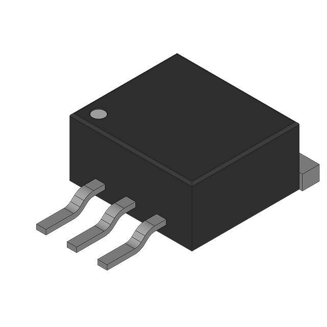
DDPAK/TO-263 (3)
10.18 mm × 8.41 mm
TO-220 (3)
14.986 mm × 10.16 mm
(1) For all available packages, see the orderable addendum at
the end of the datasheet.
Typical Application
1
An IMPORTANT NOTICE at the end of this data sheet addresses availability, warranty, changes, use in safety-critical applications,
intellectual property matters and other important disclaimers. PRODUCTION DATA.
�LM1085
SNVS038H – JULY 1999 – REVISED JANUARY 2015
www.ti.com
Table of Contents
1
2
3
4
5
6
7
Features ..................................................................
Applications ...........................................................
Description .............................................................
Revision History.....................................................
Pin Configuration and Functions .........................
Specifications.........................................................
1
1
1
2
3
4
6.1
6.2
6.3
6.4
6.5
6.6
4
4
4
4
5
7
Absolute Maximum Ratings ......................................
ESD Ratings ............................................................
Recommended Operating Conditions.......................
Thermal Information ..................................................
Electrical Characteristics...........................................
Typical Characteristics ..............................................
Detailed Description .............................................. 9
7.1 Overview ................................................................... 9
7.2 Functional Block Diagram ......................................... 9
7.3 Feature Description................................................. 10
7.4 Device Functional Modes........................................ 11
8
Application and Implementation ........................ 13
8.1 Application Information............................................ 13
8.2 Typical Applications ................................................ 13
9 Power Supply Recommendations...................... 20
10 Layout................................................................... 20
10.1 Layout Guidelines ................................................. 20
10.2 Layout Example .................................................... 20
10.3 Thermal Considerations ........................................ 20
11 Device and Documentation Support ................. 22
11.1
11.2
11.3
11.4
Documentation Support ........................................
Trademarks ...........................................................
Electrostatic Discharge Caution ............................
Glossary ................................................................
22
22
22
22
12 Mechanical, Packaging, and Orderable
Information ........................................................... 22
4 Revision History
NOTE: Page numbers for previous revisions may differ from page numbers in the current version.
Changes from Revision H (March 2013) to Revision I
•
Added ESD Ratings table, Feature Description section, Device Functional Modes, Application and Implementation
section, Power Supply Recommendations section, Layout section, Device and Documentation Support section, and
Mechanical, Packaging, and Orderable Information section ................................................................................................. 4
Changes from Revision F (March 2013) to Revision G
•
2
Page
Page
Deleted layout of National Data Sheet to TI format.............................................................................................................. 19
Submit Documentation Feedback
Copyright © 1999–2015, Texas Instruments Incorporated
Product Folder Links: LM1085
�LM1085
www.ti.com
SNVS038H – JULY 1999 – REVISED JANUARY 2015
5 Pin Configuration and Functions
3-Pin
TO-220
Top View
3-Pin
DDPAK/TO-263
Top View
Pin Functions
PIN
NAME
NO.
I/O
DESCRIPTION
ADJ/GND
1
-
Adjust pin for the adjustable output voltage version. Ground pin for the fixed output voltage
versions.
OUTPUT
2
O
Output voltage pin for the regulator.
INPUT
3
I
Input voltage pin for the regulator.
Submit Documentation Feedback
Copyright © 1999–2015, Texas Instruments Incorporated
Product Folder Links: LM1085
3
�LM1085
SNVS038H – JULY 1999 – REVISED JANUARY 2015
www.ti.com
6 Specifications
6.1 Absolute Maximum Ratings
over operating free-air temperature range (unless otherwise noted)
(1) (2)
MIN
MAX
UNIT
LM1085-ADJ
29
V
LM1085-12
18
V
LM1085-3.3
27
V
25
V
Maximum Input to Output Voltage Differential
LM1085-5.0
Power Dissipation
(3)
Internally Limited
Junction Temperature (TJ) (4)
Lead Temperature
Storage temperature range, Tstg
(1)
(2)
(3)
(4)
–65
V
150
°C
260, to 10 sec
°C
150
°C
Stresses beyond those listed under Absolute Maximum Ratings may cause permanent damage to the device. These are stress ratings
only, which do not imply functional operation of the device at these or any other conditions beyond those indicated under Recommended
Operating Conditions. Exposure to absolute-maximum-rated conditions for extended periods may affect device reliability.
If Military/Aerospace specified devices are required, please contact the Texas Instruments Sales Office/ Distributors for availability and
specifications.
Power dissipation is kept in a safe range by current limiting circuitry. Refer to Overload Recovery.
The maximum power dissipation is a function of TJ(max) , θJA, and TA. The maximum allowable power dissipation at any ambient
temperature is PD = (TJ(max)–T A)/θJA. All numbers apply for packages soldered directly into a PC board. Refer to Thermal
Considerations in the Application Notes.
6.2 ESD Ratings
V(ESD)
(1)
Human-body model (HBM), per ANSI/ESDA/JEDEC JS-001 (1)
Electrostatic discharge
VALUE
UNIT
±2000
V
JEDEC document JEP155 states that 500-V HBM allows safe manufacturing with a standard ESD control process.
6.3 Recommended Operating Conditions
over operating free-air temperature range (unless otherwise noted)
Junction Temperature (TJ) (1)
(1)
MIN
MAX
UNIT
−40
125
°C
The maximum power dissipation is a function of TJ(max) , θJA, and TA. The maximum allowable power dissipation at any ambient
temperature is PD = (TJ(max)–T A)/θJA. All numbers apply for packages soldered directly into a PC board. Refer to Thermal
Considerations in the Application Notes.
6.4 Thermal Information
LM1085
THERMAL METRIC (1)
KTT
NDE
3 PINS
3 PINS
RθJA
Junction-to-ambient thermal resistance
40.6
22.8
RθJC(top)
Junction-to-case (top) thermal resistance
43.0
15.6
RθJB
Junction-to-board thermal resistance
23.1
4.2
ψJT
Junction-to-top characterization parameter
9.9
2.2
ψJB
Junction-to-board characterization parameter
22.1
4.2
RθJC(bot)
Junction-to-case (bottom) thermal resistance
0.7
0.7
(1)
4
UNIT
°C/W
For more information about traditional and new thermal metrics, see the IC Package Thermal Metrics application report, SPRA953.
Submit Documentation Feedback
Copyright © 1999–2015, Texas Instruments Incorporated
Product Folder Links: LM1085
�LM1085
www.ti.com
SNVS038H – JULY 1999 – REVISED JANUARY 2015
6.5 Electrical Characteristics
Minimum and Maximum limits are ensured through test, design, or statistical correlation. Typical values represent the most
likely parametric norm at TJ = 25°C, and are provided for reference purposes only.
MIN (1)
TYP (2)
MAX (1)
LM1085-ADJ, IOUT = 10 mA, VIN − VOUT = 3 V, 10 mA ≤
IOUT ≤ IFULL LOAD,1.5 V ≤ (VIN−VOUT) ≤ 15 V
1.238
1.250
1.262
LM1085-ADJ, IOUT = 10 mA, VIN − VOUT = 3 V, 10 mA ≤
IOUT ≤ IFULL LOAD,1.5 V ≤ (VIN − VOUT) ≤ 15 V, –40°C ≤ TJ
≤ 125°C
1.225
1.250
1.270
LM1085-3.3, IOUT = 0 mA, VIN = 5 V, 0 ≤ IOUT ≤ IFULL
LOAD, 4.8 V ≤ VIN ≤ 15 V
3.270
3.300
3.330
LM1085-3.3, IOUT = 0 mA, VIN = 5 V, 0 ≤ IOUT ≤ IFULL
LOAD, 4.8 V ≤ VIN ≤ 15 V, –40°C ≤ TJ ≤ 125°C
3.235
3.300
3.365
LM1085-5.0, IOUT = 0 mA, VIN = 8 V, 0 ≤ IOUT ≤ IFULL
LOAD, 6.5 V ≤ VIN ≤ 20 V
4.950
5.000
5.050
LM1085-5.0, IOUT = 0 mA, VIN = 8 V, 0 ≤ IOUT ≤ IFULL
LOAD, 6.5 V ≤ VIN ≤ 20 V, –40°C ≤ TJ ≤ 125°C
4.900
5.000
5.100
LM1085-12, IOUT = 0 mA, VIN = 15 V, 0 ≤ IOUT ≤ IFULL
LOAD, 13.5 V ≤ VIN ≤ 25 V
11.880
12.000
12.120
LM1085-12, IOUT = 0 mA, VIN = 15 V, 0 ≤ IOUT ≤ IFULL
LOAD, 13.5 V ≤ VIN ≤ 25 V, –40°C ≤ TJ ≤ 125°C
11.760
12.000
12.240
LM1085-ADJ, IOUT =10 mA, 1.5 V ≤ (VIN-VOUT) ≤ 15 V
0.015
0.2
LM1085-ADJ, IOUT =10 mA, 1.5 V ≤ (VIN-VOUT) ≤ 15 V,
–40°C ≤ TJ ≤ 125°C
0.035
0.2
LM1085-3.3, IOUT = 0 mA, 4.8 V ≤ VIN ≤ 15 V
0.5
6
LM1085-3.3, IOUT = 0 mA, 4.8 V ≤ VIN ≤ 15 V, –40°C ≤
TJ ≤ 125°C
1.0
6
LM1085-5.0, IOUT = 0 mA, 6.5 V ≤ VIN ≤ 20 V
0.5
10
LM1085-5.0, IOUT = 0 mA, 6.5 V ≤ VIN ≤ 20 V, –40°C ≤
TJ ≤ 125°C
1.0
10
LM1085-12, I OUT = 0 mA, 13.5 V ≤ VIN ≤ 25 V
1.0
25
LM1085-12, I OUT = 0 mA, 13.5 V ≤ VIN ≤ 25 V, –40°C ≤
TJ ≤ 125°C
2.0
25
LM1085-ADJ, (VIN-V OUT) = 3 V, 10 mA ≤ IOUT ≤ IFULL
0.1
0.3
0.2
0.4
LM1085-3.3, VIN = 5 V, 0 ≤ IOUT ≤ IFULL LOAD
3
15
LM1085-3.3, VIN = 5 V, 0 ≤ IOUT ≤ IFULL LOAD, –40°C ≤ TJ
≤ 125°C
7
20
LM1085-5.0, VIN = 8 V, 0 ≤ IOUT ≤ IFULL LOAD
5
20
LM1085-5.0, VIN = 8 V, 0 ≤ IOUT ≤ IFULL LOAD, –40°C ≤ TJ
≤ 125°C
10
35
LM1085-12, VIN = 15 V, 0 ≤ IOUT ≤ IFULL LOAD
12
36
LM1085-12, VIN = 15 V, 0 ≤ IOUT ≤ IFULL LOAD, –40°C ≤
TJ ≤ 125°C
24
72
LM1085-ADJ, 3.3, 5, 12, ΔVREF, ΔVOUT = 1%, IOUT = 3A,
–40°C ≤ TJ ≤ 125°C
1.3
1.5
PARAMETER
VREF
VOUT
ΔVOUT
TEST CONDITIONS
Reference Voltage
(3)
Output Voltage
(3)
Line Regulation
(4)
UNIT
V
V
V
V
mV
mV
mV
LOAD
LM1085-ADJ, (VIN-V OUT) = 3 V, 10 mA ≤ IOUT ≤ IFULL
LOAD, –40°C ≤ TJ ≤ 125°C
ΔVOUT
VDO
(1)
(2)
(3)
(4)
(5)
Load Regulation
(4)
Dropout Voltage
(5)
mV
mV
mV
V
All limits are specified by testing or statistical analysis.
Typical Values represent the most likely parametric norm.
IFULL LOAD is defined in the current limit curves. The IFULL LOAD Curve defines the current limit as a function of input-to-output voltage.
Note that 30W power dissipation for the LM1085 is only achievable over a limited range of input-to-output voltage.
Load and line regulation are measured at constant junction temperature, and are ensured up to the maximum power dissipation of 30W.
Power dissipation is determined by the input/output differential and the output current. Ensured maximum power dissipation will not be
available over the full input/output range.
Dropout voltage is specified over the full output current range of the device.
Submit Documentation Feedback
Copyright © 1999–2015, Texas Instruments Incorporated
Product Folder Links: LM1085
5
�LM1085
SNVS038H – JULY 1999 – REVISED JANUARY 2015
www.ti.com
Electrical Characteristics (continued)
Minimum and Maximum limits are ensured through test, design, or statistical correlation. Typical values represent the most
likely parametric norm at TJ = 25°C, and are provided for reference purposes only.
MIN (1)
TYP (2)
LM1085-ADJ, VIN−VOUT = 5 V, –40°C ≤ TJ ≤ 125°C
3.2
5.5
LM1085-ADJ, VIN−VOUT = 25 V, –40°C ≤ TJ ≤ 125°C
0.2
0.5
LM1085-3.3, VIN = 8.0 V, –40°C ≤ TJ ≤ 125°C
3.2
5.5
A
LM1085-5.0, VIN = 10 V, –40°C ≤ TJ ≤ 125°C
3.2
5.5
A
LM1085-12, VIN = 17 V, –40°C ≤ TJ ≤ 125°C
3.2
5.5
A
PARAMETER
ILIMIT
Current Limit
Minimum Load
Current (6)
IGND
Quiescent Current
Thermal Regulation
Ripple Rejection
(6)
6
TEST CONDITIONS
MAX (1)
UNIT
A
LM1085-ADJ, VIN −VOUT = 25 V, –40°C ≤ TJ ≤ 125°C
5.0
10.0
mA
LM1085-3.3, VIN ≤ 18 V, –40°C ≤ TJ ≤ 125°C
5.0
10.0
mA
LM1085-5.0, VIN ≤ 20 V, –40°C ≤ TJ ≤ 125°C
5.0
10.0
mA
LM1085-12, VIN ≤ 25 V, –40°C ≤ TJ ≤ 125°C
5.0
10.0
mA
.004
0.02
%/W
TA = 25°C, 30ms Pulse
fRIPPLE = 120Hz, COUT = 25µF Tantalum, IOUT = 3A,
LM1085-ADJ, CADJ = 25µF, (VIN−VO) = 3 V, –40°C ≤ TJ
≤ 125°C
60
75
LM1085-3.3, VIN = 6.3 V, –40°C ≤ TJ ≤ 125°C
60
72
dB
LM1085-5.0, VIN = 8.0 V, –40°C ≤ TJ ≤ 125°C
60
68
dB
LM1085-12, VIN = 15 V, –40°C ≤ TJ ≤ 125°C
54
60
dB
LM1085–ADJ
dB
55
IADJ
Adjust Pin Current
ΔIADJ
Adjust Pin Current
Change
LM1085–ADJ, 10mA ≤ IOUT ≤ IFULL LOAD, 1.5 V ≤
VIN−VOUT ≤ 25 V, –40°C ≤ TJ ≤ 125°C
0.2
Temperature Stability
–40°C ≤ TJ ≤ 125°C
0.5
Long Term Stability
TA= 125°C, 1000 Hrs
0.3
RMS Output Noise
(% of VOUT)
10Hz ≤ f ≤ 10 kHz
LM1085–ADJ, –40°C ≤ TJ ≤ 125°C
120
5
µA
µA
1.0
0.003
The minimum output current required to maintain regulation.
Submit Documentation Feedback
Copyright © 1999–2015, Texas Instruments Incorporated
Product Folder Links: LM1085
�LM1085
www.ti.com
SNVS038H – JULY 1999 – REVISED JANUARY 2015
6.6 Typical Characteristics
Figure 1. Dropout Voltage vs Output Current
Figure 2. Short-Circuit Current vs Input/Output Difference
Figure 3. Percent Change in Output Voltage vs Temperature
Figure 4. Adjust Pin Current vs Temperature
Figure 5. Maximum Power Dissipation vs Temperature
Figure 6. Ripple Rejection vs Frequency (LM1085-Adj.)
Submit Documentation Feedback
Copyright © 1999–2015, Texas Instruments Incorporated
Product Folder Links: LM1085
7
�LM1085
SNVS038H – JULY 1999 – REVISED JANUARY 2015
www.ti.com
Typical Characteristics (continued)
Figure 7. Ripple Rejection vs Output Current (LM1085-ADJ)
Figure 8. Line Transient Response
Figure 9. Load Transient Response
8
Submit Documentation Feedback
Copyright © 1999–2015, Texas Instruments Incorporated
Product Folder Links: LM1085
�LM1085
www.ti.com
SNVS038H – JULY 1999 – REVISED JANUARY 2015
7 Detailed Description
7.1 Overview
A basic functional diagram for the LM1085-ADJ (excluding protection circuitry) is shown in Figure 10. The
topology is basically that of the LM317 except for the pass transistor. Instead of a Darlington NPN with its two
diode voltage drop, the LM1085 uses a single NPN. This results in a lower dropout voltage. The structure of the
pass transistor is also known as a quasi LDO. The advantage of a quasi LDO over a PNP LDO is its inherently
lower quiescent current. The LM1085 is ensured to provide a minimum dropout voltage of 1.5V over temperature,
at full load.
Figure 10. Basic Functional Diagram for the LM1085, Excluding Protection Circuitry
7.2 Functional Block Diagram
Submit Documentation Feedback
Copyright © 1999–2015, Texas Instruments Incorporated
Product Folder Links: LM1085
9
�LM1085
SNVS038H – JULY 1999 – REVISED JANUARY 2015
www.ti.com
7.3 Feature Description
7.3.1 Ripple Rejection
Ripple rejection is a function of the open loop gain within the feed-back loop (refer to and Figure 13). The
LM1085 exhibits 75dB of ripple rejection (typ.). When adjusted for voltages higher than VREF, the ripple rejection
decreases as function of adjustment gain: (1+R1/R2) or VO/VREF. Therefore a 5V adjustment decreases ripple
rejection by a factor of four (−12dB); Output ripple increases as adjustment voltage increases.
However, the adjustable version allows this degradation of ripple rejection to be compensated. The adjust
terminal can be bypassed to ground with a capacitor (CADJ). The impedance of the CADJ should be equal to or
less than R1 at the desired ripple frequency. This bypass capacitor prevents ripple from being amplified as the
output voltage is increased.
1/(2π*fRIPPLE*CADJ) ≤ R1
(1)
7.3.2 Load Regulation
The LM1085 regulates the voltage that appears between its output and ground pins, or between its output and
adjust pins. In some cases, line resistances can introduce errors to the voltage across the load. To obtain the
best load regulation, a few precautions are needed.
Figure 11 shows a typical application using a fixed output regulator. Rt1 and Rt2 are the line resistances. VLOAD
is less than the VOUT by the sum of the voltage drops along the line resistances. In this case, the load regulation
seen at the RLOAD would be degraded from the data sheet specification. To improve this, the load should be tied
directly to the output terminal on the positive side and directly tied to the ground terminal on the negative side.
Figure 11. Typical Application Using Fixed Output Regulator
When the adjustable regulator is used (Figure 12), the best performance is obtained with the positive side of the
resistor R1 tied directly to the output terminal of the regulator rather than near the load. This eliminates line drops
from appearing effectively in series with the reference and degrading regulation. For example, a 5V regulator with
0.05Ω resistance between the regulator and load will have a load regulation due to line resistance of 0.05Ω x IL.
If R1 (= 125Ω) is connected near the load the effective line resistance will be 0.05Ω (1 + R2/R1) or in this case, it
is 4 times worse. In addition, the ground side of the resistor R2 can be returned near the ground of the load to
provide remote ground sensing and improve load regulation.
Figure 12. Best Load Regulation Using Adjustable Output Regulator
10
Submit Documentation Feedback
Copyright © 1999–2015, Texas Instruments Incorporated
Product Folder Links: LM1085
�LM1085
www.ti.com
SNVS038H – JULY 1999 – REVISED JANUARY 2015
Feature Description (continued)
7.3.3 Overload Recovery
Overload recovery refers to regulator's ability to recover from a short circuited output. A key factor in the recovery
process is the current limiting used to protect the output from drawing too much power. The current limiting circuit
reduces the output current as the input to output differential increases. Refer to short circuit curve in the Typical
Characteristics section.
During normal start-up, the input to output differential is small since the output follows the input. But, if the output
is shorted, then the recovery involves a large input to output differential. Sometimes during this condition the
current limiting circuit is slow in recovering. If the limited current is too low to develop a voltage at the output, the
voltage will stabilize at a lower level. Under these conditions it may be necessary to recycle the power of the
regulator in order to get the smaller differential voltage and thus adequate start up conditions. Refer to Typical
Characteristics section for the short circuit current vs. input differential voltage.
7.4 Device Functional Modes
7.4.1 Output Voltage
The LM1085 adjustable version develops a 1.25V reference voltage, (VREF), between the output and the adjust
terminal. As shown in Figure 13, this voltage is applied across resistor R1 to generate a constant current I1. This
constant current then flows through R2. The resulting voltage drop across R2 adds to the reference voltage to
sets the desired output voltage.
The current IADJ from the adjustment terminal introduces an output error. But since it is small (120uA max), it
becomes negligible when R1 is in the 100 Ω range.
For fixed voltage devices, R1 and R2 are integrated inside the devices.
Figure 13. Basic Adjustable Regulator
7.4.2 Stability Consideration
Stability consideration primarily concerns the phase response of the feedback loop. In order for stable operation,
the loop must maintain negative feedback. The LM1085 requires a certain amount series resistance with
capacitive loads. This series resistance introduces a zero within the loop to increase phase margin and thus
increase stability. The equivalent series resistance (ESR) of solid tantalum or aluminum electrolytic capacitors is
used to provide the appropriate zero (approximately 500 kHz).
Aluminum electrolytics are less expensive than tantalums, but their ESR varies exponentially at cold
temperatures; therefore requiring close examination when choosing the desired transient response over
temperature. Tantalums are a convenient choice because their ESR varies less than 2:1 over temperature.
The recommended load/decoupling capacitance is a 10uF tantalum or a 50uF aluminum. These values will
assure stability for the majority of applications.
The adjustable versions allow an additional capacitor to be used at the ADJ pin to increase ripple rejection. If this
is done the output capacitor should be increased to 22 uF for tantalum or to 150 uF for aluminum.
Capacitors other than tantalum or aluminum can be used at the adjust pin and the input pin. A 10uF capacitor is
a reasonable value at the input. See Ripple Rejection section regarding the value for the adjust pin capacitor.
Submit Documentation Feedback
Copyright © 1999–2015, Texas Instruments Incorporated
Product Folder Links: LM1085
11
�LM1085
SNVS038H – JULY 1999 – REVISED JANUARY 2015
www.ti.com
Device Functional Modes (continued)
It is desirable to have large output capacitance for applications that entail large changes in load current
(microprocessors for example). The higher the capacitance, the larger the available charge per demand. It is also
desirable to provide low ESR to reduce the change in output voltage:
V = ΔI x ESR
(2)
It is common practice to use several tantalum and ceramic capacitors in parallel to reduce this change in the
output voltage by reducing the overall ESR.
Output capacitance can be increased indefinitely to improve transient response and stability.
7.4.3 Protection Diodes
Under normal operation, the LM1085 regulator does not need any protection diode. With the adjustable device,
the internal resistance between the adjustment and output terminals limits the current. No diode is needed to
divert the current around the regulator even with a capacitor on the adjustment terminal. The adjust pin can take
a transient signal of ±25 V with respect to the output voltage without damaging the device.
When an output capacitor is connected to a regulator and the input is shorted, the output capacitor will discharge
into the output of the regulator. The discharge current depends on the value of the capacitor, the output voltage
of the regulator, and rate of decrease of VIN. In the LM1085 regulator, the internal diode between the output and
input pins can withstand microsecond surge currents of 10 A to 20 A. With an extremely large output capacitor
(≥1000 µf), and with input instantaneously shorted to ground, the regulator could be damaged. In this case, an
external diode is recommended between the output and input pins to protect the regulator, shown in Figure 14.
Figure 14. Regulator With Protection Diode
12
Submit Documentation Feedback
Copyright © 1999–2015, Texas Instruments Incorporated
Product Folder Links: LM1085
�LM1085
www.ti.com
SNVS038H – JULY 1999 – REVISED JANUARY 2015
8 Application and Implementation
NOTE
Information in the following applications sections is not part of the TI component
specification, and TI does not warrant its accuracy or completeness. TI’s customers are
responsible for determining suitability of components for their purposes. Customers should
validate and test their design implementation to confirm system functionality.
8.1 Application Information
The LM1085 is versatile in its applications, including uses in programmable output regulation and local on-card
regulation. Or, by connecting a fixed resistor between the ADJUST and OUTPUT terminals, the LM1085 can
function as a precision current regulator. An optional output capacitor can be added to improve transient
response. The ADJUST terminal can be bypassed to achieve very high ripple-rejection ratios, which are difficult
to achieve with standard three-terminal regulators. Please note, in the following applications, if ADJ is mentioned,
it makes use of the adjustable version of the part, however, if GND is mentioned, it is the fixed voltage version of
the part.
8.2 Typical Applications
8.2.1 1.2-V to 15-V Adjustable Regulator
This part can be used as a simple low drop out regulator to enable a variety of output voltages needed for
demanding applications. By using an adjustable R2 resistor a variety of output voltages can be made possible as
shown in Figure 15 based on the LM1085-ADJ.
Figure 15. 1.2-V to 15-V Adjustable Regulator
8.2.1.1 Design Requirements
The device component count is very minimal, employing two resistors as part of a voltage divider circuit and an
output capacitor for load regulation.
8.2.1.2 Detailed Design Procedure
The voltage divider for this part is set based on the equation in Figure 15, where R1 is the upper feedback
resistor R2 is the lower feedback resistor.
Submit Documentation Feedback
Copyright © 1999–2015, Texas Instruments Incorporated
Product Folder Links: LM1085
13
�LM1085
SNVS038H – JULY 1999 – REVISED JANUARY 2015
www.ti.com
Typical Applications (continued)
8.2.1.3 Application Curve
8.2.2 Adjustable at 5 V
The application shown in Figure 16 outlines a simple 5 V output application made possible by the LM1085-ADJ.
This application can provide 3 A at high efficiencies and very low drop-out.
Figure 16. Adjustable @ 5V
14
Submit Documentation Feedback
Copyright © 1999–2015, Texas Instruments Incorporated
Product Folder Links: LM1085
�LM1085
www.ti.com
SNVS038H – JULY 1999 – REVISED JANUARY 2015
Typical Applications (continued)
8.2.3 5-V Regulator with Shutdown
A variation of the 5 V output regulator application with shutdown control is shown in Figure 17 based on the
LM1085-ADJ. It uses a simple NPN transistor on the ADJ pin to block or sink the current on the ADJ pin. If the
TTL logic is pulled high, the NPN transistor is activated and the part is disabled, outputting approximately 1.25 V.
If the TTL logic is pulled low, the NPN transistor is unbiased and the regulator functions normally.
Figure 17. 5-V Regulator with Shutdown
8.2.4 Battery Charger
The LM1085-ADJ can be used as a battery charger to regulate the charging current required by the battery bank
as shown in Figure 18. In this application the LM1085 acts as a constant voltage, constant current part by
sensing the voltage potential across the battery and compensating it to the current voltage. To maintain this
voltage, the regulator delivers the maximum charging current required to charge the battery. As the battery
approaches the fully charged state, the potential drop across the sense resistor, RS, reduces and the regulator
throttles back the current to maintain the float voltage of the battery.
Figure 18. Battery Charger
Submit Documentation Feedback
Copyright © 1999–2015, Texas Instruments Incorporated
Product Folder Links: LM1085
15
�LM1085
SNVS038H – JULY 1999 – REVISED JANUARY 2015
www.ti.com
Typical Applications (continued)
8.2.5 Adjustable Fixed Regulator
A simple adjustable, fixed range output regulator can be made possible by placing a variable resistor on the
ground of the device as shown in Figure 19 based on the fixed output voltage LM1085-5.0. The GND pin has a
small quiescent current of 5 mA typical. Increasing the resistance on the GND pin increases the voltage potential
across the resistor. This potential is then mirrored on to the output to increase the total output voltage by the
potential drop across the GND resistor.
Figure 19. Adjustable Fixed Regulator
8.2.6 Regulator with Reference
A fixed output voltage version of the LM1085-5.0 can be employed to provide an output rail and a reference rail
at the same time as shown in Figure 20. This simple application makes use of a reference diode, the LM136-5,
to regulate the GND voltage to a fixed 5 V based on the quiescent current generated by the GND pin. This
voltage is then added onto the output to generate a total of 10 V out.
Figure 20. Regulator With Reference
16
Submit Documentation Feedback
Copyright © 1999–2015, Texas Instruments Incorporated
Product Folder Links: LM1085
�LM1085
www.ti.com
SNVS038H – JULY 1999 – REVISED JANUARY 2015
Typical Applications (continued)
8.2.7 High Current Lamp Driver Protection
A simple constant current source with protection can be designed by controlling the impedance between the
lamp and ground. The LM1085-ADJ shown in Figure 21 makes use of an external TTL or CMOS input to drive
the NPN transistor. This pulls the output of the regulator to a few tenths of a volt and puts the part into current
limit. Releasing the logic will reduce the current flow across the lamp into the normal operating current thereby
protecting the lamp during startup.
Figure 21. High Current Lamp Driver Protection
8.2.8 Battery Backup Regulated Supply
A regulated battery backup supply can be generated by using two fixed output voltage versions of the part as
shown in Figure 22. The top regulator supplies the Line voltage during normal operation, however when the input
is not available, the second regulator derives power from the battery backup and regulates it to 5 V based on the
LM1085-5.0. The diodes prevent the rails from back feeding into the supply and batteries.
Figure 22. Battery Backup Regulated Supply
Submit Documentation Feedback
Copyright © 1999–2015, Texas Instruments Incorporated
Product Folder Links: LM1085
17
�LM1085
SNVS038H – JULY 1999 – REVISED JANUARY 2015
www.ti.com
Typical Applications (continued)
8.2.9 Ripple Rejection Enhancement
A very simple ripple rejection circuit is shown in Figure 23 using the LM1085-ADJ. The capacitor C1 smooths out
the ripple on the output by cleaning up the feedback path and preventing excess noise from feeding back into the
regulator. Please remember XC1 should be approximately equal to R1 at the ripple frequency.
Figure 23. Ripple Rejection Enhancement
8.2.10 Automatic Light Control
A common street light control or automatic light control circuit is designed in Figure 24 based on the LM1085ADJ. The photo transistor conducts in the presence of light and grounds the ADJ pin preventing the lamp from
turning on. However, in the absence of light, the LM1085 regulates the voltage to 1.25V between OUT and ADJ,
ensuring the lamp remains on.
Figure 24. Automatic Light Control
18
Submit Documentation Feedback
Copyright © 1999–2015, Texas Instruments Incorporated
Product Folder Links: LM1085
�LM1085
www.ti.com
SNVS038H – JULY 1999 – REVISED JANUARY 2015
Typical Applications (continued)
8.2.11 Generating Negative Supply Voltage
A quick inverting output rail or negative output rail is shown in Figure 25 using the LM1085 fixed output part. By
tying the output to GND, the GND node is at a relatively more negative potential than the output. This is then
interfaced to the negative application such as an operational amplifier or any other rail needing negative voltage.
Figure 25. Generating Negative Supply Voltage
8.2.12 Remote Sensing
Remote sensing is a method of compensating the output voltage to a very precise degree by sensing the output
and feeding it back through the feedback. The circuit implementing this is shown in Figure 26 using the LM1085ADJ. The output of the regulator is fed into a voltage follower to avoid any loading effects and the output of the
op-amp is injected into the top of the feedback resistor network. This has the effect of modulating the voltage to a
precise degree without additional loading on the output.
Figure 26. Remote Sensing
Submit Documentation Feedback
Copyright © 1999–2015, Texas Instruments Incorporated
Product Folder Links: LM1085
19
�LM1085
SNVS038H – JULY 1999 – REVISED JANUARY 2015
www.ti.com
9 Power Supply Recommendations
The linear regulator input supply should be well regulated and kept at a voltage level such that the maximum
input to output voltage differential allowed by the device is not exceeded. The minimum dropout voltage (VIN –
VOUT) should be met with extra headroom when possible in order to keep the output well regulated. A 10 μF or
higher capacitor should be placed at the input to bypass noise.
10 Layout
10.1 Layout Guidelines
For the best overall performance, some layout guidelines should be followed. Place all circuit components on the
same side of the circuit board and as near as practical to the respective linear regulator pins connections. Traces
should be kept short and wide to reduce the amount of parasitic elements into the system. The actual width and
thickness of traces will depend on the current carrying capability and heat dissipation required by the end
system. An array of plated vias can be placed on the pad area underneath the TAB to conduct heat to any inner
plane areas or to a bottom-side copper plane.
10.2 Layout Example
Figure 27. Layout Example
10.3 Thermal Considerations
ICs heats up when in operation, and power consumption is one factor in how hot it gets. The other factor is how
well the heat is dissipated. Heat dissipation is predictable by knowing the thermal resistance between the IC and
ambient (θJA). Thermal resistance has units of temperature per power (C/W). The higher the thermal resistance,
the hotter the IC.
The LM1085 specifies the thermal resistance for each package as junction to case (θJC). In order to get the total
resistance to ambient (θJA), two other thermal resistance must be added, one for case to heat-sink (θCH) and one
for heatsink to ambient (θHA). The junction temperature can be predicted as follows:
TJ = TA + PD (θJC + θCH + θHA) = TA + PD θJA
(3)
TJ is junction temperature, TA is ambient temperature, and PD is the power consumption of the device. Device
power consumption is calculated as follows:
20
Submit Documentation Feedback
Copyright © 1999–2015, Texas Instruments Incorporated
Product Folder Links: LM1085
�LM1085
www.ti.com
SNVS038H – JULY 1999 – REVISED JANUARY 2015
Thermal Considerations (continued)
IIN = IL + IG
PD = (VIN−VOUT) IL + VINIG
(4)
(5)
Figure 28 shows the voltages and currents which are present in the circuit.
Figure 28. Power Dissipation Diagram
Once the devices power is determined, the maximum allowable (θJA (max)) is calculated as:
θJA (max) = TR(max)/PD = TJ(max) − TA(max)/PD
The LM1085 has different temperature specifications for two different sections of the IC: the control section and
the output section. The Thermal Information table shows the junction to case thermal resistances for each of
these sections, while the maximum junction temperatures (TJ(max)) for each section is listed in the Absolute
Maximum Ratings section of the datasheet. TJ(max) is 125°C for the control section, while TJ(max) is 150°C for the
output section.
θJA (max) should be calculated separately for each section as follows:
θJA (max, CONTROL SECTION) = (125°C - TA(max))/PD
θJA (max, OUTPUT SECTION) = (150°C - TA(max))/PD
(6)
(7)
The required heat sink is determined by calculating its required thermal resistance (θHA (max)).
θHA (max) = θJA (max) − (θJC + θCH)
(θHA
(max))
(θHA
(θHA
(8)
should also be calculated twice as follows:
= θJA (max, CONTROL SECTION) - (θJC (CONTROL SECTION) + θCH)
)
(max) = θJA(max, OUTPUT SECTION) - (θJC (OUTPUT SECTION) + θCH)
(max))
(9)
(10)
If thermal compound is used, θCH can be estimated at 0.2 C/W. If the case is soldered to the heat sink, then a
θCH can be estimated as 0 C/W.
After, θHA (max) is calculated for each section, choose the lower of the two θHA
appropriate heat sink.
(max)
values to determine the
If PC board copper is going to be used as a heat sink, then Figure 29 can be used to determine the appropriate
area (size) of copper foil required.
Figure 29. Heat Sink Thermal Resistance vs Area
Submit Documentation Feedback
Copyright © 1999–2015, Texas Instruments Incorporated
Product Folder Links: LM1085
21
�LM1085
SNVS038H – JULY 1999 – REVISED JANUARY 2015
www.ti.com
11 Device and Documentation Support
11.1 Documentation Support
11.1.1 Related Documentation
Application Note 1520 A Guide to Board Layout for Best Thermal Resistance for Exposed Packages, SNVA183
11.2 Trademarks
All trademarks are the property of their respective owners.
11.3 Electrostatic Discharge Caution
These devices have limited built-in ESD protection. The leads should be shorted together or the device placed in conductive foam
during storage or handling to prevent electrostatic damage to the MOS gates.
11.4 Glossary
SLYZ022 — TI Glossary.
This glossary lists and explains terms, acronyms, and definitions.
12 Mechanical, Packaging, and Orderable Information
The following pages include mechanical, packaging, and orderable information. This information is the most
current data available for the designated devices. This data is subject to change without notice and revision of
this document. For browser-based versions of this data sheet, refer to the left-hand navigation.
22
Submit Documentation Feedback
Copyright © 1999–2015, Texas Instruments Incorporated
Product Folder Links: LM1085
�PACKAGE OPTION ADDENDUM
www.ti.com
30-Sep-2021
PACKAGING INFORMATION
Orderable Device
Status
(1)
Package Type Package Pins Package
Drawing
Qty
Eco Plan
(2)
Lead finish/
Ball material
MSL Peak Temp
Op Temp (°C)
Device Marking
(3)
(4/5)
(6)
LM1085IS-12/NOPB
ACTIVE
DDPAK/
TO-263
KTT
3
45
RoHS-Exempt
& Green
SN
Level-3-245C-168 HR
-40 to 125
LM1085
IS-12
LM1085IS-3.3
NRND
DDPAK/
TO-263
KTT
3
45
Non-RoHS
& Green
Call TI
Level-3-235C-168 HR
-40 to 125
LM1085
IS-3.3
LM1085IS-3.3/NOPB
ACTIVE
DDPAK/
TO-263
KTT
3
45
RoHS-Exempt
& Green
SN
Level-3-245C-168 HR
-40 to 125
LM1085
IS-3.3
LM1085IS-5.0/NOPB
ACTIVE
DDPAK/
TO-263
KTT
3
45
RoHS-Exempt
& Green
SN
Level-3-245C-168 HR
-40 to 125
LM1085
IS-5.0
LM1085IS-ADJ
NRND
DDPAK/
TO-263
KTT
3
45
Non-RoHS
& Green
Call TI
Level-3-235C-168 HR
LM1085IS-ADJ/NOPB
ACTIVE
DDPAK/
TO-263
KTT
3
45
RoHS-Exempt
& Green
SN
Level-3-245C-168 HR
LM1085ISX-3.3
NRND
DDPAK/
TO-263
KTT
3
500
Non-RoHS
& Green
Call TI
Level-3-235C-168 HR
LM1085ISX-3.3/NOPB
ACTIVE
DDPAK/
TO-263
KTT
3
500
RoHS-Exempt
& Green
SN
Level-3-245C-168 HR
-40 to 125
LM1085
IS-3.3
LM1085ISX-5.0/NOPB
ACTIVE
DDPAK/
TO-263
KTT
3
500
RoHS-Exempt
& Green
SN
Level-3-245C-168 HR
-40 to 125
LM1085
IS-5.0
LM1085ISX-ADJ
NRND
DDPAK/
TO-263
KTT
3
500
Non-RoHS
& Green
Call TI
Level-3-235C-168 HR
-40 to 125
LM1085
IS-ADJ
LM1085ISX-ADJ/NOPB
ACTIVE
DDPAK/
TO-263
KTT
3
500
RoHS-Exempt
& Green
SN
Level-3-245C-168 HR
-40 to 125
LM1085
IS-ADJ
LM1085IT-12/NOPB
ACTIVE
TO-220
NDE
3
45
RoHS & Green
SN
Level-1-NA-UNLIM
-40 to 125
LM1085
IT-12
LM1085IT-3.3/NOPB
ACTIVE
TO-220
NDE
3
45
RoHS & Green
SN
Level-1-NA-UNLIM
-40 to 125
LM1085
IT-3.3
LM1085IT-5.0
NRND
TO-220
NDE
3
45
Non-RoHS
& Green
Call TI
Level-1-NA-UNLIM
LM1085IT-5.0/NOPB
ACTIVE
TO-220
NDE
3
45
RoHS & Green
SN
Level-1-NA-UNLIM
-40 to 125
LM1085
IT-5.0
LM1085IT-ADJ
NRND
TO-220
NDE
3
45
Non-RoHS
& Green
Call TI
Level-1-NA-UNLIM
-40 to 125
LM1085
IT-ADJ
LM1085IT-ADJ/NOPB
ACTIVE
TO-220
NDE
3
45
RoHS & Green
SN
Level-1-NA-UNLIM
-40 to 125
LM1085
Addendum-Page 1
LM1085
IS-ADJ
-40 to 125
LM1085
IS-ADJ
LM1085
IS-3.3
LM1085
IT-5.0
Samples
�PACKAGE OPTION ADDENDUM
www.ti.com
Orderable Device
30-Sep-2021
Status
(1)
Package Type Package Pins Package
Drawing
Qty
Eco Plan
(2)
Lead finish/
Ball material
MSL Peak Temp
Op Temp (°C)
Device Marking
(3)
(4/5)
(6)
IT-ADJ
(1)
The marketing status values are defined as follows:
ACTIVE: Product device recommended for new designs.
LIFEBUY: TI has announced that the device will be discontinued, and a lifetime-buy period is in effect.
NRND: Not recommended for new designs. Device is in production to support existing customers, but TI does not recommend using this part in a new design.
PREVIEW: Device has been announced but is not in production. Samples may or may not be available.
OBSOLETE: TI has discontinued the production of the device.
(2)
RoHS: TI defines "RoHS" to mean semiconductor products that are compliant with the current EU RoHS requirements for all 10 RoHS substances, including the requirement that RoHS substance
do not exceed 0.1% by weight in homogeneous materials. Where designed to be soldered at high temperatures, "RoHS" products are suitable for use in specified lead-free processes. TI may
reference these types of products as "Pb-Free".
RoHS Exempt: TI defines "RoHS Exempt" to mean products that contain lead but are compliant with EU RoHS pursuant to a specific EU RoHS exemption.
Green: TI defines "Green" to mean the content of Chlorine (Cl) and Bromine (Br) based flame retardants meet JS709B low halogen requirements of