Product
Folder
Sample &
Buy
Technical
Documents
Tools &
Software
Support &
Community
LM10
SNOSBH4E – MAY 1998 – REVISED OCTOBER 2015
LM10 Operational Amplifier and Voltage Reference
1 Features
•
•
•
•
•
•
1
Input Offset Voltage: 2 mV (Maximum)
Input Offset Current: 0.7 nA (Maximum)
Input Bias Current: 20 nA (Maximum)
Reference Regulation: 0.1% (Maximum)
Offset Voltage Drift: 2 μV/°C
Reference Drift: 0.002%/°C
2 Applications
•
•
•
•
Remote Amplifiers
Battery-Level Indicators
Thermocouple Transmitters
Voltage and Current regulators
3 Description
The LM10 series are monolithic linear ICs consisting
of a precision reference, an adjustable reference
buffer and an independent, high-quality operational
amplifier.
The unit can operate from a total supply voltage as
low as 1.1 V or as high as 40 V, drawing only 270 μA.
A complementary output stage swings within 15 mV
of the supply terminals or will deliver ±20-mA output
current with ±0.4-V saturation. Reference output can
be as low as 200 mV.
The circuit is recommended for portable equipment
and is completely specified for operation from a
single power cell. In contrast, high output-drive
capability, both voltage and current, along with
thermal overload protection, suggest it in demanding
general-purpose applications.
The device is capable of operating in a floating mode,
independent of fixed supplies. It can function as a
remote comparator, signal conditioner, SCR controller
or transmitter for analog signals, delivering the
processed signal on the same line used to supply
power. It is also suited for operation in a wide range
of voltage and current regulator applications, from low
voltages to several hundred volts, providing greater
precision than existing ICs.
This series is available in the three standard
temperature ranges, with the commercial part having
relaxed limits. In addition, a low-voltage specification
(suffix L) is available in the limited temperature
ranges at a cost savings.
Device Information(1)
PART NUMBER
LM10
PACKAGE
BODY SIZE (NOM)
SOIC (14)
8.992 mm × 7.498 mm
SDIP (8)
8.255 mm × 8.255 mm
PDIP (8)
9.81 mm × 6.35 mm
(1) For all available packages, see the orderable addendum at
the end of the data sheet.
Operational Amplifier Schematic
(Pin numbers are for 8-pin packages)
1
An IMPORTANT NOTICE at the end of this data sheet addresses availability, warranty, changes, use in safety-critical applications,
intellectual property matters and other important disclaimers. PRODUCTION DATA.
�LM10
SNOSBH4E – MAY 1998 – REVISED OCTOBER 2015
www.ti.com
Table of Contents
1
2
3
4
5
6
Features ..................................................................
Applications ...........................................................
Description .............................................................
Revision History.....................................................
Pin Configuration and Functions .........................
Specifications.........................................................
6.1
6.2
6.3
6.4
6.5
6.6
6.7
6.8
7
1
1
1
2
3
4
Absolute Maximum Ratings ...................................... 4
Recommended Operating Conditions....................... 4
Thermal Information .................................................. 4
Electrical Characteristics LM10/LM10B .................... 5
Electrical Characteristics, LM10C ............................. 6
Electrical Characteristics, LM10BL ........................... 8
Electrical Characteristics, LM10CL ........................... 9
Typical Characteristics ............................................ 11
Detailed Description ............................................ 17
7.1 Overview ................................................................. 17
7.2 Functional Block Diagram ....................................... 17
7.3 Feature Description................................................. 17
7.4 Device Functional Modes........................................ 17
8
Application and Implementation ........................ 18
8.1 Application Information............................................ 18
8.2 Typical Application ................................................. 18
8.3 System Examples ................................................... 19
9 Power Supply Recommendations...................... 27
10 Layout................................................................... 27
10.1 Layout Guidelines ................................................. 27
10.2 Layout Example .................................................... 27
11 Device and Documentation Support ................. 28
11.1
11.2
11.3
11.4
11.5
11.6
Device Support ....................................................
Documentation Support ........................................
Community Resources..........................................
Trademarks ...........................................................
Electrostatic Discharge Caution ............................
Glossary ................................................................
28
28
28
29
29
29
12 Mechanical, Packaging, and Orderable
Information ........................................................... 29
4 Revision History
NOTE: Page numbers for previous revisions may differ from page numbers in the current version.
Changes from Revision D (March 2013) to Revision E
•
Added Pin Configuration and Functions section, ESD Ratings table, Feature Description section, Device Functional
Modes, Application and Implementation section, Power Supply Recommendations section, Layout section, Device
and Documentation Support section, and Mechanical, Packaging, and Orderable Information section .............................. 1
Changes from Revision C (March 2013) to Revision D
•
2
Page
Page
Changed layout of National Data Sheet to TI format ........................................................................................................... 26
Submit Documentation Feedback
Copyright © 1998–2015, Texas Instruments Incorporated
Product Folder Links: LM10
�LM10
www.ti.com
SNOSBH4E – MAY 1998 – REVISED OCTOBER 2015
5 Pin Configuration and Functions
NEV Package
8-Pin SDIP
Top View
P Package
8-Pin PDIP
Top View
Pin Functions — 8-Pin SDIP or PDIP
PIN
NAME
NO.
I/O
DESCRIPTION
Balance
5
I
Used for offset nulling
Op Amp Input (+)
3
I
Noninverting input of operational amplifier
Op Amp Input (–)
2
I
Inverting input of operational amplifier
Op Amp Output
6
O
Output terminal of operational amplifier
Reference Feedback
8
I
Feedback terminal of reference
Reference Output
1
O
Output terminal of reference
V+
7
I
Positive supply voltage
V–
4
I
Negative supply voltage
NPA Package
14-Pin SOIC
Top View
Pin Functions — 14-Pin SOIC
PIN
NAME
Balance
NC
Op Amp Input (–)
NO.
I/O
DESCRIPTION
9
I
1, 2, 7, 8, 14, 13
—
Used for offset nulling
4
I
Inverting input of operational amplifier
No connection
Op Amp Input (+)
5
I
Noninverting input of operational amplifier
Op Amp Output
10
O
Output terminal of operational amplifier
Reference Feedback
12
I
Feedback terminal of reference
Reference Output
3
O
Output terminal of reference
V+
11
I
Positive supply voltage
V–
6
I
Negative supply voltage
Submit Documentation Feedback
Copyright © 1998–2015, Texas Instruments Incorporated
Product Folder Links: LM10
3
�LM10
SNOSBH4E – MAY 1998 – REVISED OCTOBER 2015
www.ti.com
6 Specifications
6.1 Absolute Maximum Ratings
(1) (2) (3)
See
MIN
Total supply voltage
Differential input voltage (4)
Power dissipation
7
V
±40
V
LM10BL/LM10CL
±7
V
Internally limited
TO
Continuous
Soldering (10 seconds)
300
°C
Soldering (10 seconds)
260
°C
Vapor phase (60 seconds)
215
°C
Infrared (15 seconds)
220
°C
LM10
150
°C
LM10B
100
°C
LM10C
85
°C
150
°C
DIP
−55
Storage temperature, Tstg
(1)
(2)
(3)
(4)
(5)
(6)
V
LM10/LM10B/LM10C
Output short-circuit duration (6)
Maximum junction
temperature
UNIT
45
LM10BL/LM10CL
(5)
Lead temperature
MAX
LM10/LM10B/LM10C
Refer to RETS10X for LM10H military specifications.
Stresses beyond those listed under Absolute Maximum Ratings may cause permanent damage to the device. These are stress ratings
only, and functional operation of the device at these or any other conditions beyond those indicated under Recommended Operating
Conditions is not implied. Exposure to absolute-maximum-rated conditions for extended periods may affect device reliability.
If Military/Aerospace specified devices are required, please contact the TI Sales Office/Distributors for availability and specifications.
The Input voltage can exceed the supply voltages provided that the voltage from the input to any other terminal does not exceed the
maximum differential input voltage and excess dissipation is accounted for when VIN < V−.
The maximum, operating-junction temperature is 150°C for the LM10, 100°C for the LM10B(L) and 85°C for the LM10C(L). At elevated
temperatures, devices must be derated based on package thermal resistance.
Internal thermal limiting prevents excessive heating that could result in sudden failure, but the IC can be subjected to accelerated stress
with a shorted output and worst-case conditions.
6.2 Recommended Operating Conditions
over operating free-air temperature range (unless otherwise noted)
MIN
VS
Supply input voltage range (V–) – (V+)
VCM
Common-mode voltage
VREF
Reference voltage
IREF
Reference current
NOM
MAX
UNIT
1.2
40
V
(V–)
(V+) – 0.85
V
0.2
V
0
1
mA
6.3 Thermal Information
LM10
THERMAL METRIC (1)
NEV (SDIP)
NPA (SOIC)
P (PDIP)
8 PINS
14 PINS
8 PINS
UNIT
RθJA
Junction-to-ambient thermal resistance
150
90
87
°C/W
RθJC(top)
Junction-to-case (top) thermal resistance
45
—
—
°C/W
(1)
4
For more information about traditional and new thermal metrics, see the Semiconductor and IC Package Thermal Metrics application
report, SPRA953.
Submit Documentation Feedback
Copyright © 1998–2015, Texas Instruments Incorporated
Product Folder Links: LM10
�LM10
www.ti.com
SNOSBH4E – MAY 1998 – REVISED OCTOBER 2015
6.4 Electrical Characteristics LM10/LM10B
TJ=25°C unless otherwise specified (1)
PARAMETER
Input offset voltage
Input offset current (2)
Input bias current
Input resistance
TEST CONDITIONS
MIN
TJ=25°C
TMIN ≤ TJ ≤ TMAX (see
TJ=25°C
TMIN ≤ TJ ≤ TMAX (see
TJ=25°C
nA
30
TJ=25°C
250
TMIN ≤ TJ ≤ TMAX (see
(1)
)
120
(1)
)
50
(1)
20
IOUT = ±15 mA, TMIN ≤ TJ ≤ TMAX (see
(1)
20
)
)
(1)
)
(1)
)
(1)
)
(1)
)
(1)
0.1 mA ≤ IOUT ≤ 5 mA, TMIN ≤ TJ ≤ TMAX (see
)
1.5 V ≤ V ≤ 40 V, RL = 250 Ω
(1)
)
(1)
−20 V ≤ VCM ≤ 19 V, TMIN ≤ TJ ≤ TMAX (see
)
(1)
VS = ±20 V, TMIN ≤ TJ ≤ TMAX (see
)
(1)
)
V/mV
V/mV
V/mV
V/mV
1.5
3
V/mV
0.5
V/mV
0.5
V/mV
14
33
V/mV
14
33
V/mV
V/mV
25
V/mV
V/mV
93
102
dB
93
102
dB
dB
96
dB
84
(1)
)
dB
84
1 V ≤ V+ ≤ 39.8 V
1.1 V ≤ V+ ≤ 39.8 V, TMIN ≤ TJ ≤ TMAX (see
V = −0.2 V, TMIN ≤ TJ ≤ TMAX (see
130
3
90
V = 1.1 V, TMIN ≤ TJ ≤ TMAX (see
V/mV
87
−0.2 V ≥ V− ≥ −39 V
V+ = 1 V, TMIN ≤ TJ ≤ TMAX (see
kΩ
4
−20 V ≤ VCM ≤ 19.15 V
−
V/mV
1.5
8
0.1 mA ≤ IOUT ≤ 20 mA, TMIN ≤ TJ ≤ TMAX (see
+
400
6
+
(1)
)
(1)
)
dB
96
106
dB
96
106
dB
90
Offset voltage drift
Offset current drift
TC < 100°C
1.2 V ≤ VS ≤ 40 V
(1)
1.3 V ≤ VS ≤ 40 V, TMIN ≤ TJ ≤ TMAX (see
)
0 ≤ IREF ≤ 1 mA, VREF = 200 mV, TMIN ≤ TJ ≤ TMAX (see
dB
2
μV/°C
2
pA/°C
60
pA/°C
0.001
0.003
%/V
0.001
0.003
%/V
0.006
%/V
(1)
0 ≤ IREF ≤ 1 mA
)
0.01%
V+− VREF ≥ 1 V, TMIN ≤ TJ ≤ TMAX (see
(1)
V+− VREF ≥ 1.1 V, TMIN ≤ TJ ≤ TMAX (see
)
nA
kΩ
80
IOUT = ±20 mA, TMIN ≤ TJ ≤ TMAX (see
UNIT
500
150
1.3 V ≤ VOUT ≤ 40 V, RL = 1.1 kΩ, TMIN ≤ TJ ≤ TMAX (see
(2)
(3)
20
)
1.2 V ≤ VOUT ≤ 40 V, RL = 1.1 kΩ
(1)
nA
(1)
VOUT = ±0.3 V, VCM = −0.4 V, TMIN ≤ TJ ≤ TMAX (see
Load regulation
nA
1.5
10
TMIN ≤ TJ ≤ TMAX (see
VOUT = ±0.4 V, TMIN ≤ TJ ≤ TMAX (see
Line regulation
mV
0.7
)
VS = ±0.65 V, IOUT = ±2 mA, TMIN ≤ TJ ≤ TMAX (see
Bias current drift
mV
3
(1)
VS = ±0.6 V, IOUT = ±2 mA
Supply-voltage
rejection
2
0.25
VS = ±20 V, VOUT = ±19.4 V
Common-mode
rejection
0.3
)
VOUT = ±19.95 V, TMIN ≤ TJ ≤ TMAX (see
Shunt gain (3)
MAX
(1)
VS = ±20 V, IOUT = 0
Large signal voltage
gain
TYP
0.1%
0.15%
(1)
)
0.15%
These specifications apply for V− ≤ VCM ≤ V+− 0.85 V, 1 V (TMIN ≤ TJ ≤ TMAX), 1.2 V, 1.3 V (TMIN ≤ TJ ≤ TMAX) < VS ≤ VMAX, VREF = 0.2 V
and 0 ≤ IREF ≤ 1 mA, unless otherwise specified: VMAX = 40 V for the standard part and 6.5 V for the low voltage part. The fulltemperature-range operation is −55°C to 125°C for the LM10, −25°C to 85°C for the LM10B(L) and 0°C to 70°C for the LM10C(L). The
specifications do not include the effects of thermal gradients (τ1 ≃ 20 ms), die heating (τ2 ≃ 0.2 s) or package heating. Gradient effects
are small and tend to offset the electrical error (see curves).
For TJ > 90°C, IOS may exceed 1.5 nA for VCM = V−. With TJ = 125°C and V− ≤ VCM ≤ V− + 0.1 V, IOS ≤ 5 nA.
This defines operation in floating applications such as the bootstrapped regulator or two-wire transmitter. Output is connected to the V+
terminal of the IC and input common mode is referred to V− (see System Examples). Effect of larger output-voltage swings with higher
load resistance can be accounted for by adding the positive-supply rejection error.
Submit Documentation Feedback
Copyright © 1998–2015, Texas Instruments Incorporated
Product Folder Links: LM10
5
�LM10
SNOSBH4E – MAY 1998 – REVISED OCTOBER 2015
www.ti.com
Electrical Characteristics LM10/LM10B (continued)
TJ=25°C unless otherwise specified(1)
PARAMETER
TEST CONDITIONS
Amplifier gain
0.2 V ≤ VREF ≤ 35 V
Feedback sense
voltage
TJ=25°C
Feedback current
TMIN ≤ TJ ≤ TMAX (see
TJ=25°C
(1)
TMIN ≤ TJ ≤ TMAX (see
)
MIN
TYP
50
75
V/mV
195
(1)
)
200
194
20
(1)
)
205
mV
206
mV
50
nA
65
Reference drift
Supply current
0.002
TJ=25°C
TMIN ≤ TJ ≤ TMAX (see
270
(1)
)
TJ=25°C
1.2 V ≤ VS ≤ 40 V
(1)
)
400
μA
500
μA
75
TJ=25°C
1.3 V ≤ VS ≤ 40 V
15
(1)
TMIN ≤ TJ ≤ TMAX (see
)
nA
%/°C
15
TMIN ≤ TJ ≤ TMAX (see
Supply current change
UNIT
V/mV
23
TJ=25°C
TMIN ≤ TJ ≤ TMAX (see
MAX
75
μA
μA
6.5 Electrical Characteristics, LM10C
TJ=25°C unless otherwise specified (1)
PARAMETER
Input offset voltage
Input offset current (2)
Input bias current
Input resistance
TEST CONDITIONS
MIN
TJ=25°C
TMIN ≤ TJ ≤ TMAX (see
nA
)
40
150
(1)
)
80
(1)
)
15
Large signal voltage gain IOUT = ±15 mA, TMIN ≤ TJ ≤ TMAX (see
(1)
15
)
)
VS = ±0.6 V, IOUT = ±2 mA
VS = 0.65 V, IOUT = ±2 mA, TMIN ≤ TJ ≤ TMAX (see
VOUT = ±0.4 V, TMIN ≤ TJ ≤ TMAX (see
(1)
)
(1)
)
400
V/mV
(1)
)
V/mV
130
1.3 V ≤ VOUT ≤ 40 V, RL = 1.1 kΩ, TMIN ≤ TJ ≤ TMAX (see
(1)
)
V/mV
1
3
V/mV
1
3
V/mV
V/mV
)
V/mV
10
33
V/mV
10
33
V/mV
6
1.5 V ≤ V+ ≤ 40 V, RL = 250 Ω
0.1 mA ≤ IOUT ≤ 20 mA, TMIN ≤ TJ ≤ TMAX (see
(1)
6
(1)
)
V/mV
V/mV
0.75
1.2 V ≤ VOUT ≤ 40 V, RL = 1.1 kΩ
0.1 mA ≤ IOUT ≤ 5 mA, TMIN ≤ TJ ≤ TMAX (see
kΩ
0.75
VOUT = ±0.3 V, VCM = −0.4 V, TMIN ≤ TJ ≤ TMAX (see
nA
kΩ
50
25
UNIT
400
115
(1)
6
nA
30
(1)
IOUT = ±20 mA, TMIN ≤ TJ ≤ TMAX (see
(2)
(3)
nA
3
12
VS = ±20 V, VOUT = ±19.4 V
(1)
2
0.4
VOUT = ±19.95 V, TMIN ≤ TJ ≤ TMAX (see
Shunt gain
mV
)
VS = ±20 V, IOUT = 0
(3)
mV
5
(1)
TJ=25°C
TMIN ≤ TJ ≤ TMAX (see
4
)
TJ=25°C
TMIN ≤ TJ ≤ TMAX (see
MAX
0.5
(1)
TJ=25°C
TMIN ≤ TJ ≤ TMAX (see
TYP
4
V/mV
25
V/mV
V/mV
These specifications apply for V− ≤ VCM ≤ V+− 0.85 V, 1 V (TMIN ≤ TJ ≤ TMAX), 1.2 V, 1.3 V (TMIN ≤ TJ ≤ TMAX) < VS ≤ VMAX, VREF = 0.2 V
and 0 ≤ IREF ≤ 1 mA, unless otherwise specified: VMAX = 40 V for the standard part and 6.5 V for the low voltage part. The fulltemperature-range operation is −55°C to 125°C for the LM10, −25°C to 85°C for the LM10B(L) and 0°C to 70°C for the LM10C(L). The
specifications do not include the effects of thermal gradients (τ1 ≃ 20 ms), die heating (τ2 ≃ 0.2 s) or package heating. Gradient effects
are small and tend to offset the electrical error (see curves).
For TJ > 90°C, IOS may exceed 1.5 nA for VCM = V−. With TJ = 125°C and V− ≤ VCM ≤ V− + 0.1 V, IOS ≤ 5 nA.
This defines operation in floating applications such as the bootstrapped regulator or two-wire transmitter. Output is connected to the V+
terminal of the IC and input common mode is referred to V− (see System Examples). Effect of larger output-voltage swings with higher
load resistance can be accounted for by adding the positive-supply rejection error.
Submit Documentation Feedback
Copyright © 1998–2015, Texas Instruments Incorporated
Product Folder Links: LM10
�LM10
www.ti.com
SNOSBH4E – MAY 1998 – REVISED OCTOBER 2015
Electrical Characteristics, LM10C (continued)
TJ=25°C unless otherwise specified(1)
PARAMETER
TEST CONDITIONS
−20 V ≤ VCM ≤ 19.15 V
Common-mode rejection −20 V ≤ VCM ≤ 19 V
(1)
VS = ±20 V, TMIN ≤ TJ ≤ TMAX (see
)
TYP
−0.2 V ≥ V ≥ −39 V
90
102
dB
90
102
dB
87
V+ = 1 V, TMIN ≤ TJ ≤ TMAX (see
(1)
V+ = 1.1 V, TMIN ≤ TJ ≤ TMAX (see
)
)
+
(1)
1.1 V ≤ V ≤ 39.8 V, TMIN ≤ TJ ≤ TMAX (see
)
(1)
)
93
106
dB
90
TC < 100°C
1.3 V ≤ VS ≤ 40 V, TMIN ≤ TJ ≤ TMAX (see
(1)
)
+
0.008
%/V
0.001
0.008
%/V
0.01
%/V
)
0.15%
0.2%
(1)
)
0.2%
TMIN ≤ TJ ≤ TMAX (see
25
(1)
)
TJ=25°C
)
70
V/mV
200
189
TJ=25°C
V/mV
15
190
(1)
22
(1)
)
210
mV
211
mV
75
nA
90
Reference drift
Supply current
pA/°C
0.001
)
TJ=25°C
0.2 V ≤ VREF ≤ 35 V
TMIN ≤ TJ ≤ TMAX (see
pA/°C
(1)
V − VREF≥ 1.1 V, TMIN ≤ TJ ≤ TMAX (see
Feedback current
5
0.01%
V+ − VREF ≥ 1 V, TMIN ≤ TJ ≤ TMAX (see
TMIN ≤ TJ ≤ TMAX (see
μV/°C
(1)
0 ≤ IREF ≤ 1 mA
Feedback sense voltage
dB
5
90
0 ≤ IREF ≤ 1 mA, VREF = 200 mV, TMIN ≤ TJ ≤ TMAX (see
Amplifier gain
dB
dB
1.2 V ≤ VS ≤ 40 V
Load regulation
dB
106
Offset current drift
Line regulation
dB
93
Offset voltage drift
Bias current drift
96
84
1 V ≤ V+ ≤ 39.8 V
0.003
TJ=25°C
TMIN ≤ TJ ≤ TMAX (see
1.2 V ≤ VS ≤ 40 V
Supply current change
1.3 V ≤ VS ≤ 40 V
UNIT
dB
84
(1)
V− = −0.2 V, TMIN ≤ TJ ≤ TMAX (see
MAX
87
−
Supply-voltage rejection
MIN
300
(1)
)
TJ=25°C
TMIN ≤ TJ ≤ TMAX (see
)
TJ=25°C
TMIN ≤ TJ ≤ TMAX (see
500
μA
570
μA
15
(1)
75
15
(1)
)
75
Submit Documentation Feedback
Copyright © 1998–2015, Texas Instruments Incorporated
Product Folder Links: LM10
nA
%/°C
μA
μA
7
�LM10
SNOSBH4E – MAY 1998 – REVISED OCTOBER 2015
www.ti.com
6.6 Electrical Characteristics, LM10BL
TJ=25°C unless otherwise specified. (1)
PARAMETER
Input offset voltage
Input offset current (2)
Input bias current
Input resistance
TEST CONDITIONS
MIN
TJ=25°C
TMIN ≤ TJ ≤ TMAX (see
TJ=25°C
TMIN ≤ TJ ≤ TMAX (see
mV
3
mV
0.7
nA
1.5
nA
20
nA
(1)
)
TJ=25°C
10
TMIN ≤ TJ ≤ TMAX (see
(1)
)
30
TJ=25°C
250
TMIN ≤ TJ ≤ TMAX (see
(1)
)
60
(1)
)
10
)
300
V/mV
(1)
)
V/mV
V/mV
0.5
0.5
)
)
1.5 V ≤ V +≤ 6.5 V, RL = 500 Ω
8
0.1 mA ≤ IOUT ≤ 10 mA, TMIN ≤ TJ ≤ TMAX (see
(1)
)
4
(1)
89
−3.25 V ≤ VCM ≤ 2.4 V
−3.25 V ≤ VCM ≤ 2.25 V, TMIN ≤ TJ ≤ TMAX (see
)
(1)
)
V/mV
3
(1)
V/mV
V/mV
30
V/mV
V/mV
102
dB
83
−
−0.2 V ≥ V ≥ −5.4 V
86
(1)
)
(1)
)
+
1 V ≤ V ≤ 6.3 V
1.1 V ≤ V+ ≤ 6.3 V, TMIN ≤ TJ ≤ TMAX (see
V−=0.2 V, TMIN ≤ TJ ≤ TMAX (see
V/mV
1.5
VOUT = ±0.3 V, VCM = −0.4 V, TMIN ≤ TJ ≤ TMAX (see
V+ = 1.2 V, TMIN ≤ TJ ≤ TMAX (see
25
3
VOUT = ±0.4 V, VCM = −0.4 V, TMIN ≤ TJ ≤ TMAX (see
V+ = 1 V, TMIN ≤ TJ ≤ TMAX (see
V/mV
1.5
(1)
VS = ±3.25 V, TMIN ≤ TJ ≤ TMAX (see
kΩ
4
VS = ±0.6 V, IOUT = ±2 mA
(1)
)
(1)
)
nA
kΩ
40
(1)
VOUT = ±2.75 V, TMIN ≤ TJ ≤ TMAX (see
UNIT
500
150
VS = 0.65 V, IOUT = ±2 mA, TMIN ≤ TJ ≤ TMAX (see
Supply-voltage rejection
2
0.1
VS = ±3.25 V, IOUT = 10 mA
Common-mode rejection
0.3
)
VOUT = ±3.2 V, TMIN ≤ TJ ≤ TMAX (see
Shunt gain (3)
MAX
(1)
VS = ±3.25 V, IOUT = 0
Large signal voltage gain
TYP
dB
96
dB
80
dB
80
dB
94
106
dB
94
106
dB
88
dB
Offset voltage drift
2
μV/°C
Offset current drift
2
pA/°C
60
pA/°C
Bias current drift
1.2 V ≤ VS ≤ 6.5 V
Line regulation
(1)
1.3 V ≤ VS ≤ 6.5 V, TMIN ≤ TJ ≤ TMAX (see
)
0 ≤ IREF ≤ 0.5 mA, VREF = 200 mV, TMIN ≤ TJ ≤ TMAX (see
V+ − VREF ≥ 1 V, TMIN ≤ TJ ≤ TMAX (see
(1)
(2)
(3)
8
%/V
)
0.1%
0.15%
(1)
)
0.15%
TJ=25°C
0.2 V ≤ VREF ≤ 5.5 V
TMIN ≤ TJ ≤ TMAX (see
TJ=25°C
TMIN ≤ TJ ≤ TMAX (see
%/V
0.02
)
(1)
V − VREF ≥ 1.1 V, TMIN ≤ TJ ≤ TMAX (see
Feedback sense voltage
%/V
0.01
0.01%
+
Amplifier gain
0.01
0.001
(1)
0 ≤ IREF ≤ 0.5 mA
Load regulation
0.001
30
(1)
)
)
V/mV
20
195
(1)
70
194
V/mV
200
205
mV
206
mV
These specifications apply for V− ≤ VCM ≤ V+− 0.85 V, 1 V (TMIN ≤ TJ ≤ TMAX), 1.2 V, 1.3 V (TMIN ≤ TJ ≤ TMAX) < VS ≤ VMAX, VREF = 0.2 V
and 0 ≤ IREF ≤ 1 mA, unless otherwise specified: VMAX = 40 V for the standard part and 6.5 V for the low voltage part. The fulltemperature-range operation is −55°C to 125°C for the LM10, −25°C to 85°C for the LM10B(L) and 0°C to 70°C for the LM10C(L). The
specifications do not include the effects of thermal gradients (τ1 ≃ 20 ms), die heating (τ2 ≃ 0.2 s) or package heating. Gradient effects
are small and tend to offset the electrical error (see curves).
For TJ > 90°C, IOS may exceed 1.5 nA for VCM = V−. With TJ=125°C and V− ≤ VCM ≤ V−+ 0.1 V, IOS ≤ 5 nA.
This defines operation in floating applications such as the bootstrapped regulator or two-wire transmitter. Output is connected to the V+
terminal of the IC and input common mode is referred to V− (see System Examples). Effect of larger output-voltage swings with higher
load resistance can be accounted for by adding the positive-supply rejection error.
Submit Documentation Feedback
Copyright © 1998–2015, Texas Instruments Incorporated
Product Folder Links: LM10
�LM10
www.ti.com
SNOSBH4E – MAY 1998 – REVISED OCTOBER 2015
Electrical Characteristics, LM10BL (continued)
TJ=25°C unless otherwise specified.(1)
PARAMETER
Feedback current
TEST CONDITIONS
MIN
TJ=25°C
TMIN ≤ TJ ≤ TMAX (see
MAX
20
50
(1)
)
UNIT
nA
65
Reference drift
Supply current
TYP
nA
0.002
TJ=25°C
400
μA
500
μA
TYP
MAX
UNIT
0.5
4
mV
5
mV
0.2
2
nA
3
nA
12
30
nA
260
TMIN ≤ TJ ≤ TMAX (see
%/°C
(1)
)
6.7 Electrical Characteristics, LM10CL
TJ=25°C unless otherwise specified. (1)
PARAMETER
Input offset voltage
Input offset current (2)
Input bias current
Input resistance
TEST CONDITIONS
MIN
TJ=25°C
TMIN ≤ TJ ≤ TMAX (see
(1)
)
TJ=25°C
TMIN ≤ TJ ≤ TMAX (see
(1)
)
TJ=25°C
TMIN ≤ TJ ≤ TMAX (see
(1)
)
40
TJ=25°C
TMIN ≤ TJ ≤ TMAX (see
150
(1)
)
40
VOUT = ±3.2 V, TMIN ≤ TJ ≤ TMAX (see
(1)
)
5
(1)
VOUT = ±2.75 V, TMIN ≤ TJ ≤ TMAX (see
)
VS = ±0.6 V, IOUT = ±2 mA
(1)
)
V/mV
0.75
)
)
1.5 V ≤ V+ ≤ 6.5 V, RL= 500 Ω
6
0.1 mA ≤ IOUT ≤ 10 mA, TMIN ≤ TJ ≤ TMAX (see
(1)
)
−3.25 V ≤ VCM ≤ 2.25 V, TMIN ≤ TJ ≤ TMAX (see
(1)
)
(1)
)
V/mV
V/mV
30
V/mV
4
V/mV
80
102
dB
80
102
dB
74
−0.2 V ≥ V– ≥ −5.4 V
80
(1)
)
dB
96
dB
74
(1)
)
1.1 V ≤ V+ ≤ 6.3 V, TMIN ≤ TJ ≤ TMAX (see
dB
74
1 V ≤ V+ ≤ 6.3 V
V− = 0.2 V, TMIN ≤ TJ ≤ TMAX (see
V/mV
3
(1)
V = 1.2 V, TMIN ≤ TJ ≤ TMAX (see
V/mV
1
VOUT = ±0.3 V, VCM = −0.4 V, TMIN ≤ TJ ≤ TMAX (see
+
25
V/mV
0.75
V+ = 1 V, TMIN ≤ TJ ≤ TMAX (see
V/mV
3
(1)
VS = ±3.25 V, TMIN ≤ TJ ≤ TMAX (see
kΩ
1
VOUT = ±0.4 V, VCM = −0.4 V, TMIN ≤ TJ ≤ TMAX (see
−3.25 V ≤ VCM ≤ 2.4 V
Supply-voltage rejection
V/mV
3
VS = 0.65 V, IOUT = ±2 mA, TMIN ≤ TJ ≤ TMAX (see
Common-mode rejection
300
25
VS = ±3.25 V, IOUT = 10 mA
Shunt gain (3)
kΩ
115
VS = ±3.25 V, IOUT = 0
Large signal voltage gain
nA
400
(1)
)
(1)
)
dB
80
106
dB
80
106
dB
74
dB
Offset voltage drift
5
μV/°C
Offset current drift
5
pA/°C
90
pA/°C
Bias current drift
(1)
(2)
(3)
These specifications apply for V− ≤ VCM ≤ V+− 0.85 V, 1 V (TMIN ≤ TJ ≤ TMAX), 1.2 V, 1.3 V (TMIN ≤ TJ ≤ TMAX) < VS ≤ VMAX, VREF = 0.2 V
and 0 ≤ IREF ≤ 1 mA, unless otherwise specified: VMAX = 40 V for the standard part and 6.5 V for the low voltage part. The fulltemperature-range operation is −55°C to 125°C for the LM10, −25°C to 85°C for the LM10B(L) and 0°C to 70°C for the LM10C(L). The
specifications do not include the effects of thermal gradients (τ1 ≃ 20 ms), die heating (τ2 ≃ 0.2 s) or package heating. Gradient effects
are small and tend to offset the electrical error (see curves).
For TJ > 90°C, IOS may exceed 1.5 nA for VCM = V−. With TJ = 125°C and V− ≤ VCM ≤ V− + 0.1 V, IOS ≤ 5 nA.
This defines operation in floating applications such as the bootstrapped regulator or two-wire transmitter. Output is connected to the V+
terminal of the IC and input common mode is referred to V− (see System Examples). Effect of larger output-voltage swings with higher
load resistance can be accounted for by adding the positive-supply rejection error.
Submit Documentation Feedback
Copyright © 1998–2015, Texas Instruments Incorporated
Product Folder Links: LM10
9
�LM10
SNOSBH4E – MAY 1998 – REVISED OCTOBER 2015
www.ti.com
Electrical Characteristics, LM10CL (continued)
TJ=25°C unless otherwise specified.(1)
PARAMETER
TEST CONDITIONS
MIN
1.2 V ≤ VS ≤ 6.5 V
Line regulation
1.3 V ≤ VS ≤ 6.5 V, TMIN ≤ TJ ≤ TMAX (see
(1)
)
0 ≤ IREF ≤ 0.5 mA, VREF = 200 mV, TMIN ≤ TJ ≤ TMAX (see
Feedback sense voltage
Feedback current
10
%/V
0.02
%/V
0.03
%/V
)
0.15%
0.2%
(1)
)
TMIN ≤ TJ ≤ TMAX (see
0.2%
20
(1)
)
(1)
)
70
V/mV
200
189
TJ=25°C
V/mV
15
190
22
(1)
)
210
mV
211
mV
75
nA
90
Reference drift
Supply current
0.02
0.001
(1)
TJ=25°C
TMIN ≤ TJ ≤ TMAX (see
0.001
)
TJ=25°C
0.2 V ≤ VREF ≤ 5.5 V
TMIN ≤ TJ ≤ TMAX (see
UNIT
0.01%
V+− VREF ≥ 1 V, TMIN ≤ TJ ≤ TMAX (see
V+− VREF ≥ 1.1 V, TMIN ≤ TJ ≤ TMAX (see
Amplifier gain
MAX
(1)
0 ≤ IREF ≤ 0.5 mA
Load regulation
TYP
0.003
TJ=25°C
TMIN ≤ TJ ≤ TMAX (see
280
(1)
)
Submit Documentation Feedback
nA
%/°C
500
μA
570
μA
Copyright © 1998–2015, Texas Instruments Incorporated
Product Folder Links: LM10
�LM10
www.ti.com
SNOSBH4E – MAY 1998 – REVISED OCTOBER 2015
6.8 Typical Characteristics
6.8.1 Typical Characteristics (Op Amp)
Figure 1. Input Current
Figure 2. Common-Mode Limits
Figure 3. Output Voltage Drift
Figure 4. Input Noise Voltage
Figure 5. DC Voltage Gain
Figure 6. Transconductance
Submit Documentation Feedback
Copyright © 1998–2015, Texas Instruments Incorporated
Product Folder Links: LM10
11
�LM10
SNOSBH4E – MAY 1998 – REVISED OCTOBER 2015
www.ti.com
Typical Characteristics (Op Amp) (continued)
12
Figure 7. Output Saturation Characteristics
Figure 8. Output Saturation Characteristics
Figure 9. Output Saturation Characteristics
Figure 10. Minimum Supply Voltage
Figure 11. Minimum Supply Voltage
Figure 12. Minimum Supply Voltage
Submit Documentation Feedback
Copyright © 1998–2015, Texas Instruments Incorporated
Product Folder Links: LM10
�LM10
www.ti.com
SNOSBH4E – MAY 1998 – REVISED OCTOBER 2015
Typical Characteristics (Op Amp) (continued)
Figure 13. Output Impedance
Figure 14. Typical Stability Range
Figure 15. Large Signal Response
Figure 16. Comparator Response Time For Various Input
Overdrives
Figure 17. Comparator Response Time For Various Input
Overdrives
Figure 18. Follower Pulse Response
Submit Documentation Feedback
Copyright © 1998–2015, Texas Instruments Incorporated
Product Folder Links: LM10
13
�LM10
SNOSBH4E – MAY 1998 – REVISED OCTOBER 2015
www.ti.com
Typical Characteristics (Op Amp) (continued)
14
Figure 19. Noise Rejection
Figure 20. Rejection Slew Limiting
Figure 21. Supply Current
Figure 22. Thermal Gradient Feedback
Figure 23. Thermal Gradient Cross-Coupling
Figure 24. Shunt Gain
Submit Documentation Feedback
Copyright © 1998–2015, Texas Instruments Incorporated
Product Folder Links: LM10
�LM10
www.ti.com
SNOSBH4E – MAY 1998 – REVISED OCTOBER 2015
Typical Characteristics (Op Amp) (continued)
Figure 25. Shunt Gain
Figure 26. Shunt Gain
Figure 28. Shunt Gain
Figure 27. Shunt Gain
Figure 29. Shunt Gain
Submit Documentation Feedback
Copyright © 1998–2015, Texas Instruments Incorporated
Product Folder Links: LM10
15
�LM10
SNOSBH4E – MAY 1998 – REVISED OCTOBER 2015
www.ti.com
6.8.2 Typical Characteristics (Reference)
16
Figure 30. Line Regulation
Figure 31. Load Regulation
Figure 32. Reference Noise Voltage
Figure 33. Minimum Supply Voltage
Figure 34. Output Saturation
Figure 35. Typical Stability Range
Submit Documentation Feedback
Copyright © 1998–2015, Texas Instruments Incorporated
Product Folder Links: LM10
�LM10
www.ti.com
SNOSBH4E – MAY 1998 – REVISED OCTOBER 2015
7 Detailed Description
7.1 Overview
The LM10 is a dual-operational amplifier combined with a voltage reference capable of a single-supply operation
down to 1.1 V. It provides high overall performance, making it ideal for many general-purpose applications. The
circuit can also operate in a floating mode, powered by residual voltage, independent of fixed supplies and it is
well-protected from temperature drift.
7.2 Functional Block Diagram
7.3 Feature Description
7.3.1 Operating Characteristics
The LM10 is specified for operation from 1.2 V to 40 V. Many of the specifications apply from –55⁰C to 125⁰C.
Parameters that can exhibit significant variance with regard to operating voltage or temperature are presented in
electrical characteristics tables under Specifications and in the Typical Characteristics section.
7.3.2 Common-Mode Voltage Range
The input common-mode voltage range of the LM10 extends from the negative rail to 0.85 V less than the
positive rail.
7.3.3 Operational Amplifier
The minimum operating voltage is reduced to nearly one volt and the current gain is less affected by
temperature, resulting in a fairly flat bias current over temperature.
7.3.4 Voltage Reference
Second-order nonlinearities are compensated for which eliminates the bowed characteristics of conventional
designs, resulting in better temperature stability.
7.4 Device Functional Modes
7.4.1 Floating Mode
To use the device in a floating mode, the operational amplifier output is shorted to V+ which disables the PNP
portion of the output stage. Thus, with a positive input signal, neither halves of the output conducts and the
current between the supply terminals is equal to the quiescent supply current. With negative input signals, the
NPN portion of the output begins to turn on, reaching the short circuit current for a few hundred microvolts
overdrive.
7.4.2 Linear Operation
This device can also operate linearly while in the floating mode. An example of this is shown in the Typical
Application section.
Submit Documentation Feedback
Copyright © 1998–2015, Texas Instruments Incorporated
Product Folder Links: LM10
17
�LM10
SNOSBH4E – MAY 1998 – REVISED OCTOBER 2015
www.ti.com
8 Application and Implementation
NOTE
Information in the following applications sections is not part of the TI component
specification, and TI does not warrant its accuracy or completeness. TI’s customers are
responsible for determining suitability of components for their purposes. Customers should
validate and test their design implementation to confirm system functionality.
8.1 Application Information
With heavy amplifier loading to V−, resistance drops in the V− lead can adversely affect reference regulation.
Lead resistance can approach 1 Ω. Therefore, the common to the reference circuitry should be connected as
close as possible to the package.
8.2 Typical Application
* required for capacitive loading
Figure 36. Shunt Voltage Regulator
8.2.1 Design Requirements
Table 1 lists the design parameters for this example.
Table 1. Design Parameters
DESIGN PARAMETERS
EXAMPLE VALUE
Ambient Temperature Range
–55⁰C to 125⁰C
Supply Voltage Range
1.2 V to 40 V
Common-Mode Input Range
(V–) to (V+) – 0.85 V
8.2.2 Detailed Design Procedure
Given that the transfer function of this circuit is:
R
VO U T = (1 + 2 )V R E F
R1
(1)
the output can be set between 0.2 V and the breakdown voltage of the IC by selecting an appropriate value for
R2. The circuit regulates for input voltages within a saturation drop of the output (typically 0.4 V at 20 mA and
0.15 V at 5 mA). The regulator is protected from shorts or overloads by current limiting and thermal shutdown.
18
Submit Documentation Feedback
Copyright © 1998–2015, Texas Instruments Incorporated
Product Folder Links: LM10
�LM10
www.ti.com
SNOSBH4E – MAY 1998 – REVISED OCTOBER 2015
Typical regulation is about 0.05% load and 0.003%/V line. A substantial improvement in regulation can be
effected by connecting the operational amplifier as a follower and setting the reference to the desired output
voltage. This has the disadvantage that the minimum input-output differential is increased to a little more than a
diode drop. If the operational amplifier were connected for a gain of 2, the output could again saturate. But this
requires an additional pair of precision resistors.
The regulator in Figure 36 could be made adjustable to zero by connecting the operational amplifier to a
potentiometer on the reference output. This has the disadvantage that the regulation at the lower voltage settings
is not as good as it might otherwise be.
8.2.3 Application Curve
Figure 37. Frequency Response
8.3 System Examples
Circuit descriptions available in application note AN-211 (SNOA638).
8.3.1 Operational Amplifier Offset Adjustment
(Pin numbers are for 8-pin packages)
Figure 38. Standard
Figure 39. Limited Range
Submit Documentation Feedback
Copyright © 1998–2015, Texas Instruments Incorporated
Product Folder Links: LM10
19
�LM10
SNOSBH4E – MAY 1998 – REVISED OCTOBER 2015
www.ti.com
System Examples (continued)
(Pin numbers are for 8-pin packages)
Figure 40. Limited Range With Boosted Reference
8.3.2 Positive Regulators
(Pin numbers are for 8-pin packages)
Figure 41. Low Voltage
Figure 42. Best Regulation
Use only electrolytic output capacitors.
Figure 43. Zero Output
20
Figure 44. Current Regulator
Submit Documentation Feedback
Copyright © 1998–2015, Texas Instruments Incorporated
Product Folder Links: LM10
�LM10
www.ti.com
SNOSBH4E – MAY 1998 – REVISED OCTOBER 2015
System Examples (continued)
(Pin numbers are for 8-pin packages)
Required For Capacitive Loading
*Electrolytic
Figure 45. Shunt Regulator
Figure 46. Negative Regulator
*VOUT=10−4 R3
Figure 47. Precision Regulator
Figure 48. Laboratory Power Supply
Figure 49. HV Regulator
Figure 50. Protected HV Regulator
Submit Documentation Feedback
Copyright © 1998–2015, Texas Instruments Incorporated
Product Folder Links: LM10
21
�LM10
SNOSBH4E – MAY 1998 – REVISED OCTOBER 2015
www.ti.com
System Examples (continued)
(Pin numbers are for 8-pin packages)
*800°C Threshold Is Established By Connecting Balance To VREF.
*Provides Hysteresis
Figure 51. Flame Detector
Figure 52. Light Level Sensor
Figure 53. Remote Amplifier
Figure 54. Remote Thermocouple Amplifier
10 mA≤IOUT≤50 mA
500°C≤TP≤1500°C
*Gain Trim
Figure 55. Transmitter for Bridge Sensor
22
Figure 56. Precision Thermocouple Transmitter
Submit Documentation Feedback
Copyright © 1998–2015, Texas Instruments Incorporated
Product Folder Links: LM10
�LM10
www.ti.com
SNOSBH4E – MAY 1998 – REVISED OCTOBER 2015
System Examples (continued)
(Pin numbers are for 8-pin packages)
††Level-shift Trim
*Scale Factor Trim
†Copper Wire Wound
Figure 57. Resistance Thermometer Transmitter
Figure 58. Optical Pyrometer
1 mA≤IOUT≤5 mA
‡50 μA≤ID≤500 μA
††Center Scale Trim
†Scale Factor Trim
*Copper Wire Wound
200°C≤Tp≤700°C
1 mA≤IOUT≤5 mA
†Gain Trim
Figure 59. Thermocouple
Transmitter
Figure 60. Logarithmic Light Sensor
Submit Documentation Feedback
Copyright © 1998–2015, Texas Instruments Incorporated
Product Folder Links: LM10
23
�LM10
SNOSBH4E – MAY 1998 – REVISED OCTOBER 2015
www.ti.com
System Examples (continued)
(Pin numbers are for 8-pin packages)
Figure 61. Battery-level Indicator
Flashes Above 1.2V
Rate Increases With
Voltage
Figure 62. Battery-threshold Indicator
Flash Rate Increases
Above 6V and Below 15V
Figure 63. Single-cell Voltage Monitor
Figure 64. Double-ended Voltage Monitor
*Trim For Span
†Trim For Zero
INPUT
10 mV, 100nA
FULL-SCALE
Figure 65. Meter Amplifier
24
Figure 66. Thermometer
Submit Documentation Feedback
Copyright © 1998–2015, Texas Instruments Incorporated
Product Folder Links: LM10
�LM10
www.ti.com
SNOSBH4E – MAY 1998 – REVISED OCTOBER 2015
System Examples (continued)
(Pin numbers are for 8-pin packages)
ZOUT∼680Ω @ 5 kHz
AV≤1k
f1∼100 Hz
f2∼5 kHz
RL∼500
*Max Gain Trim
5
1≤λ/λ0≤10
Figure 67. Light Meter
Figure 68. Microphone Amplifier
†Controls “Loop Gain”
*Optional Frequency Shaping
Figure 69. Isolated Voltage Sensor
Figure 70. Light-Level Controller
Submit Documentation Feedback
Copyright © 1998–2015, Texas Instruments Incorporated
Product Folder Links: LM10
25
�LM10
SNOSBH4E – MAY 1998 – REVISED OCTOBER 2015
www.ti.com
System Examples (continued)
(Pin numbers are for 8-pin packages)
8.3.3 Reference and Internal Regulator
Figure 71. Reference and Internal Regulator
26
Submit Documentation Feedback
Copyright © 1998–2015, Texas Instruments Incorporated
Product Folder Links: LM10
�LM10
www.ti.com
SNOSBH4E – MAY 1998 – REVISED OCTOBER 2015
9 Power Supply Recommendations
The LM10 is specified for operation from 1.2 V to 40 V unless otherwise stated. Many specifications apply from
–55⁰C to 125⁰C. Parameters that can exhibit significant variance with regard to operating voltage or temperature
are presented in the Specifications section.
CAUTION
Supply voltages larger than 40 V can permanently damage the device; see the
Absolute Maximum Ratings table.
10 Layout
10.1 Layout Guidelines
For best operational performance of the device, good printed-circuit board (PCB) layout practices are
recommended. Low-loss, 0.1-uF bypass capacitors should be connected between each supply pin and ground,
placed as close to the device as possible. A single bypass capacitor from V+ to ground is applicable to singlesupply applications.
10.2 Layout Example
1
AMP_IN+
AMP_IN+
2
AMP_IN+
8
AMP_IN+
AMP_IN+
7
VOUT
VOUT
VOUT
AMP_IN+
AMP_IN+
AM
6
VOUT
IN
P_
–
3
AMP_IN+
AMP_1–
4
V–
1
VOUT
2
VOUT
2
AMP-IN–
1
AMP_INT–
2
AMP-IN–
BAL
1
V+
V–
Figure 72. Layout Example
Submit Documentation Feedback
Copyright © 1998–2015, Texas Instruments Incorporated
Product Folder Links: LM10
27
�LM10
SNOSBH4E – MAY 1998 – REVISED OCTOBER 2015
www.ti.com
11 Device and Documentation Support
11.1 Device Support
11.1.1 Device Nomenclature
11.1.1.1 Definition of Terms
Input offset voltage: That voltage which must be applied between the input terminals to bias the unloaded
output in the linear region.
Input offset current: The difference in the currents at the input terminals when the unloaded output is in the
linear region.
Input bias current: The absolute value of the average of the two input currents.
Input resistance: The ratio of the change in input voltage to the change in input current on either input with the
other grounded.
Large signal voltage gain: The ratio of the specified output voltage swing to the change in differential input
voltage required to produce it.
Shunt gain: The ratio of the specified output voltage swing to the change in differential input voltage required to
produce it with the output tied to the V+ terminal of the IC. The load and power source are
connected between the V+ and V− terminals, and input common-mode is referred to the V− terminal.
Common-mode rejection: The ratio of the input voltage range to the change in offset voltage between the
extremes.
Supply-voltage rejection: The ratio of the specified supply-voltage change to the change in offset voltage
between the extremes.
Line regulation: The average change in reference output voltage over the specified supply voltage range.
Load regulation: The change in reference output voltage from no load to that load specified.
Feedback sense voltage: The voltage, referred to V−, on the reference feedback terminal while operating in
regulation.
Reference amplifier gain: The ratio of the specified reference output change to the change in feedback sense
voltage required to produce it.
Feedback current: The absolute value of the current at the feedback terminal when operating in regulation.
Supply current: The current required from the power source to operate the amplifier and reference with their
outputs unloaded and operating in the linear range.
11.2 Documentation Support
11.2.1 Related Documentation
For related documentation, see the following:
AN-211 New Op Amp Ideas, SNOA638
11.3 Community Resources
The following links connect to TI community resources. Linked contents are provided "AS IS" by the respective
contributors. They do not constitute TI specifications and do not necessarily reflect TI's views; see TI's Terms of
Use.
TI E2E™ Online Community TI's Engineer-to-Engineer (E2E) Community. Created to foster collaboration
among engineers. At e2e.ti.com, you can ask questions, share knowledge, explore ideas and help
solve problems with fellow engineers.
Design Support TI's Design Support Quickly find helpful E2E forums along with design support tools and
contact information for technical support.
28
Submit Documentation Feedback
Copyright © 1998–2015, Texas Instruments Incorporated
Product Folder Links: LM10
�LM10
www.ti.com
SNOSBH4E – MAY 1998 – REVISED OCTOBER 2015
11.4 Trademarks
E2E is a trademark of Texas Instruments.
All other trademarks are the property of their respective owners.
11.5 Electrostatic Discharge Caution
These devices have limited built-in ESD protection. The leads should be shorted together or the device placed in conductive foam
during storage or handling to prevent electrostatic damage to the MOS gates.
11.6 Glossary
SLYZ022 — TI Glossary.
This glossary lists and explains terms, acronyms, and definitions.
12 Mechanical, Packaging, and Orderable Information
The following pages include mechanical, packaging, and orderable information. This information is the most
current data available for the designated devices. This data is subject to change without notice and revision of
this document. For browser-based versions of this data sheet, refer to the left-hand navigation.
Submit Documentation Feedback
Copyright © 1998–2015, Texas Instruments Incorporated
Product Folder Links: LM10
29
�PACKAGE OPTION ADDENDUM
www.ti.com
10-May-2022
PACKAGING INFORMATION
Orderable Device
Status
(1)
Package Type Package Pins Package
Drawing
Qty
Eco Plan
(2)
Lead finish/
Ball material
MSL Peak Temp
Op Temp (°C)
Device Marking
(3)
Samples
(4/5)
(6)
LM10BH
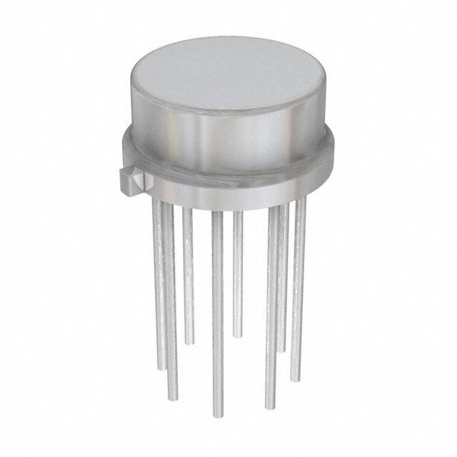
ACTIVE
TO-CAN
LMG
8
500
Non-RoHS &
Non-Green
Call TI
Call TI
-40 to 85
( LM10BH, LM10BH)
Samples
LM10BH/NOPB
ACTIVE
TO-CAN
LMG
8
500
RoHS & Green
Call TI
Level-1-NA-UNLIM
-40 to 85
( LM10BH, LM10BH)
Samples
LM10CH
ACTIVE
TO-CAN
LMG
8
500
Non-RoHS &
Non-Green
Call TI
Call TI
0 to 70
( LM10CH, LM10CH)
Samples
LM10CH/NOPB
ACTIVE
TO-CAN
LMG
8
500
RoHS & Green
Call TI
Level-1-NA-UNLIM
0 to 70
( LM10CH, LM10CH)
Samples
LM10CLN/NOPB
ACTIVE
PDIP
P
8
40
RoHS & Green
NIPDAU
Level-1-NA-UNLIM
0 to 70
LM10CLN
Samples
LM10CN/NOPB
ACTIVE
PDIP
P
8
40
RoHS & Green
NIPDAU
Level-1-NA-UNLIM
0 to 70
LM
10CN
Samples
LM10CWM
NRND
SOIC
NPA
14
50
Non-RoHS
& Green
Call TI
Level-2A-220C-4
WEEK
0 to 70
LM10CWM
LM10CWM/NOPB
ACTIVE
SOIC
NPA
14
50
RoHS & Green
SN
Level-3-260C-168 HR
0 to 70
LM10CWM
Samples
LM10CWMX/NOPB
ACTIVE
SOIC
NPA
14
1000
RoHS & Green
SN
Level-3-260C-168 HR
0 to 70
LM10CWM
Samples
(1)
The marketing status values are defined as follows:
ACTIVE: Product device recommended for new designs.
LIFEBUY: TI has announced that the device will be discontinued, and a lifetime-buy period is in effect.
NRND: Not recommended for new designs. Device is in production to support existing customers, but TI does not recommend using this part in a new design.
PREVIEW: Device has been announced but is not in production. Samples may or may not be available.
OBSOLETE: TI has discontinued the production of the device.
(2)
RoHS: TI defines "RoHS" to mean semiconductor products that are compliant with the current EU RoHS requirements for all 10 RoHS substances, including the requirement that RoHS substance
do not exceed 0.1% by weight in homogeneous materials. Where designed to be soldered at high temperatures, "RoHS" products are suitable for use in specified lead-free processes. TI may
reference these types of products as "Pb-Free".
RoHS Exempt: TI defines "RoHS Exempt" to mean products that contain lead but are compliant with EU RoHS pursuant to a specific EU RoHS exemption.
Green: TI defines "Green" to mean the content of Chlorine (Cl) and Bromine (Br) based flame retardants meet JS709B low halogen requirements of