Product
Folder
Sample &
Buy
Technical
Documents
Support &
Community
Tools &
Software
Reference
Design
LM1117
SNOS412N – FEBRUARY 2000 – REVISED JANUARY 2016
LM1117 800-mA Low-Dropout Linear Regulator
1 Features
3 Description
•
The LM1117 is a low dropout voltage regulator with a
dropout of 1.2 V at 800 mA of load current.
1
•
•
•
•
•
•
Available in 1.8 V, 2.5 V, 3.3 V, 5 V, and
Adjustable Versions
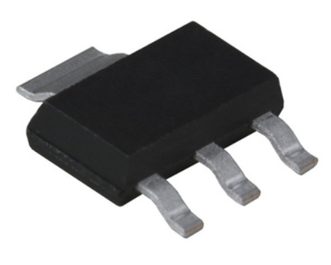
Space-Saving SOT-223 and WSON Packages
Current Limiting and Thermal Protection
Output Current 800 mA
Line Regulation 0.2% (Maximum)
Load Regulation 0.4% (Maximum)
Temperature Range
– LM1117: 0°C to 125°C
– LM1117I: −40°C to 125°C
2 Applications
•
•
•
•
•
Post Regulator for Switching DC–DC Converter
High Efficiency Linear Regulators
Battery Chargers
Portable Instrumentation
Active SCSI Termination Regulator
The LM1117 is available in an adjustable version,
which can set the output voltage from 1.25 to 13.8 V
with only two external resistors. In addition, it is
available in five fixed voltages, 1.8 V, 2.5 V, 3.3 V,
and 5 V.
The LM1117 offers current limiting and thermal
shutdown. Its circuit includes a Zener trimmed
bandgap reference to assure output voltage accuracy
to within ±1%.
A minimum of 10-µF tantalum capacitor is required at
the output to improve the transient response and
stability.
Device Information(1)
PART NUMBER
LM1117,
LM1117I
PACKAGE
BODY SIZE (NOM)
SOT-223 (4)
6.50 mm × 3.50 mm
TO-220 (3)
14.986 mm × 10.16 mm
TO-252 (3)
6.58 mm × 6.10 mm
WSON (8)
4.00 mm × 4.00 mm
TO-263 (3)
10.18 mm × 8.41 mm
(1) For all available packages, see the orderable addendum at
the end of the data sheet.
Adjustable Output Regulator
1
An IMPORTANT NOTICE at the end of this data sheet addresses availability, warranty, changes, use in safety-critical applications,
intellectual property matters and other important disclaimers. PRODUCTION DATA.
�LM1117
SNOS412N – FEBRUARY 2000 – REVISED JANUARY 2016
www.ti.com
Table of Contents
1
2
3
4
5
6
7
Features ..................................................................
Applications ...........................................................
Description .............................................................
Revision History.....................................................
Pin Configuration and Functions .........................
Specifications.........................................................
1
1
1
2
3
4
6.1
6.2
6.3
6.4
6.5
6.6
6.7
4
4
4
4
5
7
9
Absolute Maximum Ratings ......................................
ESD Ratings..............................................................
Recommended Operating Conditions.......................
Thermal Information ..................................................
LM1117 Electrical Characteristics.............................
LM1117I Electrical Characteristics............................
Typical Characteristics ..............................................
Detailed Description ............................................ 11
7.1 Overview ................................................................. 11
7.2 Functional Block Diagram ....................................... 11
7.3 Feature Description................................................. 11
7.4 Device Functional Modes........................................ 12
8
Application and Implementation ........................ 14
8.1 Application Information............................................ 14
8.2 Typical Application .................................................. 14
8.3 System Examples ................................................... 16
9 Power Supply Recommendations...................... 17
10 Layout................................................................... 17
10.1 Layout Guidelines ................................................. 17
10.2 Layout Example .................................................... 21
11 Device and Documentation Support ................. 22
11.1
11.2
11.3
11.4
Community Resources..........................................
Trademarks ...........................................................
Electrostatic Discharge Caution ............................
Glossary ................................................................
22
22
22
22
12 Mechanical, Packaging, and Orderable
Information ........................................................... 22
4 Revision History
NOTE: Page numbers for previous revisions may differ from page numbers in the current version.
Changes from Revision M (March 2013) to Revision N
Page
•
Added Pin Configuration and Functions section, ESD Ratings table, Feature Description section, Device Functional
Modes, Application and Implementation section, Power Supply Recommendations section, Layout section, Device
and Documentation Support section, and Mechanical, Packaging, and Orderable Information section .............................. 1
•
Removed LM1117-N-2.85 option after part became inactive................................................................................................. 1
•
Removed TO-263 Pinout Side View image ........................................................................................................................... 3
Changes from Revision L (July 2012) to Revision M
•
2
Page
Changed layout of National Data Sheet to TI format ........................................................................................................... 16
Submit Documentation Feedback
Copyright © 2000–2016, Texas Instruments Incorporated
Product Folder Links: LM1117
�LM1117
www.ti.com
SNOS412N – FEBRUARY 2000 – REVISED JANUARY 2016
5 Pin Configuration and Functions
DCY Package
4-Pin SOT
Top View
KTT Package
3-Pin TO-263
Top View
NDE Package
3-Pin TO-220
Top View
NDP Package
3-Pin TO-252
Top View
NGN Package
8-Pin WSON
Top View
ADJ/GND
1
VIN
2
8
NOT CONNECTED
7
VOUT
VOUT
VIN
3
6
VOUT
VIN
4
5
VOUT
When using the WSON package
Pins 2, 3 and 4 must be connected together and
Pins 5, 6 and 7 must be connected together
Pin Functions
PIN
NAME
I/O
DESCRIPTION
TO-252
WSON
SOT-223
TO-263
TO-220
ADJ/GND
1
1
1
1
1
—
VIN
3
2, 3, 4
3
3
3
I
Input voltage pin for the regulator
2 , TAB
5, 6, 7,
TAB
2, 4
2, TAB
2, TAB
O
Output voltage pin for the regulator
VOUT
Adjust pin for adjustable output option. Ground pin for fixed
output option.
Submit Documentation Feedback
Copyright © 2000–2016, Texas Instruments Incorporated
Product Folder Links: LM1117
3
�LM1117
SNOS412N – FEBRUARY 2000 – REVISED JANUARY 2016
www.ti.com
6 Specifications
6.1 Absolute Maximum Ratings
over operating free-air temperature range (unless otherwise noted) (1)
MIN
Maximum Input Voltage (VIN to GND)
Power Dissipation
(2)
(2)
V
150
TO-220 (T) Package, 10 s
260
SOT-223 (MP) Package, 4 s
260
Storage Temperature, Tstg
(1)
UNIT
20
Internally Limited
Junction Temperature (TJ) (2)
Lead Temperature
MAX
–65
°C
°C
150
°C
Stresses beyond those listed under Absolute Maximum Ratings may cause permanent damage to the device. These are stress ratings
only, which do not imply functional operation of the device at these or any other conditions beyond those indicated under Recommended
Operating Conditions. Exposure to absolute-maximum-rated conditions for extended periods may affect device reliability.
The maximum power dissipation is a function of TJ(max) , RθJA, and TA. The maximum allowable power dissipation at any ambient
temperature is PD = (TJ(max)–TA)/RθJA. All numbers apply for packages soldered directly into a PCB.
6.2 ESD Ratings
V(ESD)
(1)
Human-body model (HBM), per ANSI/ESDA/JEDEC JS-001 (1)
Electrostatic discharge
VALUE
UNIT
±2000
V
JEDEC document JEP155 states that 500-V HBM allows safe manufacturing with a standard ESD control process. Pins listed as ±2000
V may actually have higher performance.
6.3 Recommended Operating Conditions
over operating free-air temperature range (unless otherwise noted)
MIN
Input Voltage (VIN to GND)
Junction Temperature (TJ) (1)
(1)
MAX
UNIT
15
V
°C
LM1117
0
125
LM1117I
−40
125
The maximum power dissipation is a function of TJ(max) , RθJA, and TA. The maximum allowable power dissipation at any ambient
temperature is PD = (TJ(max)–TA)/RθJA. All numbers apply for packages soldered directly into a PCB.
6.4 Thermal Information
LM1117, LM1117I
THERMAL METRIC
(1)
DCY
(SOT-223)
NDE
(TO-220)
NDP
(TO-252)
NGN
(WSON)
KTT
(TO-263)
UNIT
4 PINS
3 PINS
3 PINS
8 PINS
3 PINS
RθJA
Junction-to-ambient thermal resistance
61.6
23.8
45.1
39.3
41.3
°C/W
RθJC(top)
Junction-to-case (top) thermal resistance
42.5
16.6
52.1
31.4
44.1
°C/W
RθJB
Junction-to-board thermal resistance
10.4
5.3
29.8
16.5
24.2
°C/W
ψJT
Junction-to-top characterization parameter
2.9
3.1
4.5
0.3
10.9
°C/W
ψJB
Junction-to-board characterization parameter
10.3
5.3
29.4
16.7
23.2
°C/W
RθJC(bot)
Junction-to-case (bottom) thermal resistance
—
1.5
1.3
5.6
1.3
°C/W
(1)
4
For more information about traditional and new thermal metrics, see the Semiconductor and IC Package Thermal Metrics application
report, SPRA953.
Submit Documentation Feedback
Copyright © 2000–2016, Texas Instruments Incorporated
Product Folder Links: LM1117
�LM1117
www.ti.com
SNOS412N – FEBRUARY 2000 – REVISED JANUARY 2016
6.5 LM1117 Electrical Characteristics
unless otherwise specified, TJ = 25°C.
PARAMETER
TEST CONDITIONS
LM1117-ADJ
IOUT = 10 mA, VIN – VOUT = 2 V, TJ = 25°C
VREF
Reference Voltage
LM1117-ADJ
10 mA ≤ IOUT ≤ 800 mA, 1.4 V ≤
VIN – VOUT ≤ 10 V
over the junction temperature range
0°C to 125°C
VOUT
Output Voltage
over the junction temperature range
0°C to 125°C
over the junction temperature range
0°C to 125°C
LM1117-5.0
IOUT = 10 mA, VIN = 7 V, TJ = 25°C
Line Regulation (3)
TJ = 25°C
LM1117-ADJ
IOUT = 10mA, 1.5V ≤ VIN-VOUT ≤
13.75V
TJ = 25°C
LM1117-3.3
IOUT = 0 mA, 4.75 V ≤ VIN ≤ 15 V
LM1117-5.0
IOUT = 0 mA, 6.5 V ≤ VIN ≤ 15 V
LM1117-ADJ
VIN – VOUT = 3 V, 10 ≤ IOUT ≤ 800
mA
LM1117-1.8
VIN = 3.2 V, 0 ≤ IOUT ≤ 800 mA
ΔVOUT
Load Regulation (3)
LM1117-2.5
VIN = 3.9 V, 0 ≤ IOUT ≤ 800 mA
LM1117-3.3
VIN = 4.75 V, 0 ≤ IOUT ≤ 800 mA
LM1117-5.0
VIN = 6.5 V, 0 ≤ IOUT ≤ 800 mA
(1)
(2)
(3)
1.262
1.25
1.225
1.782
over the junction temperature range
0°C to 125°C
1.27
1.8
1.746
2.475
2.5
2.45
3.3
3.235
5
4.9
0.2%
1
6
over the junction temperature range
0°C to 125°C
mV
1
6
mV
1
6
mV
1
10
mV
0.2%
0.4%
1
10
mV
1
10
mV
1
over the junction temperature range
0°C to 125°C
TJ = 25°C
V
0.035%
over the junction temperature range
0°C to 125°C
TJ = 25°C
5.05
5.1
over the junction temperature range
0°C to 125°C
TJ = 25°C
V
5
over the junction temperature range
0°C to 125°C
TJ = 25°C
3.333
3.365
over the junction temperature range
0°C to 125°C
TJ = 25°C
V
3.3
over the junction temperature range
0°C to 125°C
TJ = 25°C
2.525
2.55
over the junction temperature range
0°C to 125°C
TJ = 25°C
V
2.5
over the junction temperature range
0°C to 125°C
TJ = 25°C
1.818
1.854
over the junction temperature range
0°C to 125°C
TJ = 25°C
UNIT
V
1.8
4.95
LM1117-5.0
0 ≤ IOUT ≤ 800 mA, 6.5 V ≤ VIN ≤
12 V
LM1117-2.5
IOUT = 0 mA, 3.9 V ≤ VIN ≤ 10 V
1.25
3.267
TJ = 25°C
LM1117-3.3
0 ≤ IOUT ≤ 800 mA, 4.75 V ≤ VIN ≤ over the junction temperature range
10 V
0°C to 125°C
ΔVOUT
1.238
TJ = 25°C
LM1117-3.3
IOUT = 10 mA, VIN = 5 V TJ = 25°C
LM1117-1.8
IOUT = 0 mA, 3.2 V ≤ VIN ≤ 10 V
MAX (1)
TJ = 25°C
LM1117-2.5
IOUT = 10 mA, VIN = 4.5 V, TJ = 25°C
LM1117-2.5
0 ≤ IOUT ≤ 800 mA, 3.9 V ≤ VIN ≤
10 V
TYP (2)
TJ = 25°C
LM1117-1.8
IOUT = 10 mA, VIN = 3.8 V, TJ = 25°C
LM1117-1.8
0 ≤ IOUT ≤ 800 mA, 3.2 V ≤ VIN ≤
10 V
MIN (1)
10
mV
1
15
mV
All limits are ensured by testing or statistical analysis.
Typical Values represent the most likely parametric normal.
Load and line regulation are measured at constant junction room temperature.
Submit Documentation Feedback
Copyright © 2000–2016, Texas Instruments Incorporated
Product Folder Links: LM1117
5
�LM1117
SNOS412N – FEBRUARY 2000 – REVISED JANUARY 2016
www.ti.com
LM1117 Electrical Characteristics (continued)
unless otherwise specified, TJ = 25°C.
PARAMETER
MIN (1)
TEST CONDITIONS
TJ = 25°C
IOUT = 100 mA
VIN – V
over the junction temperature range
0°C to 125°C
OUT
IOUT = 500 mA
1.2
1.25
TJ = 25°C
ILIMIT
Current Limit
Minimum Load
Current (5)
VIN – VOUT = 5 V, TJ = 25°C
Adjust Pin Current
Change
(5)
6
mA
mA
mA
5
10
mA
5
over the junction temperature range
0°C to 125°C
10
TJ = 25°C
mA
5
over the junction temperature range
0°C to 125°C
10
TA = 25°C, 30-ms pulse
0.01
TJ = 25°C
0.1
mA
%/W
75
over the junction temperature range
0°C to 125°C
TJ = 25°C
dB
60
60
over the junction temperature range 0°C to 125°C
120
TJ = 25°C
μA
0.2
over the junction temperature range
0°C to 125°C
Temperature Stability
(4)
10
TJ = 25°C
10 ≤ IOUT ≤ 80 0mA,
1.4 V ≤ VIN – VOUT ≤ 10 V
V
5
over the junction temperature range
0°C to 125°C
fRIPPLE = 1 20 Hz, VIN – VOUT = 3
V VRIPPLE = 1 VPP
1500
5
TJ = 25°C
LM1117-5.0
VIN ≤ 15 V
Adjust Pin Current
1200
over the junction temperature range
0°C to 125°C
LM1117-3.3
VIN ≤ 15 V
V
1.7
TJ = 25°C
Quiescent Current
Ripple Regulation
800
over the junction temperature range
0°C to 125°C
LM1117-2.5
VIN ≤ 15 V
Thermal Regulation
1.3
TJ = 25°C
LM1117-1.8
VIN ≤ 15 V
V
1.2
over the junction temperature range
0°C to 125°C
LM1117-ADJ
VIN = 15 V
UNIT
1.15
over the junction temperature range
0°C to 125°C
IOUT = 800 mA
MAX (1)
1.1
TJ = 25°C
Dropout Voltage (4)
TYP (2)
5
µA
0.5%
Long Term Stability
TA = 125°C, 1000 Hrs
RMS Output Noise
(% of VOUT), 10 Hz ≤ f ≤ 10 kHz
0.3%
0.003%
The dropout voltage is the input/output differential at which the circuit ceases to regulate against further reduction in input voltage. It is
measured when the output voltage has dropped 100 mV from the nominal value obtained at VIN = VOUT + 1.5 V.
The minimum output current required to maintain regulation.
Submit Documentation Feedback
Copyright © 2000–2016, Texas Instruments Incorporated
Product Folder Links: LM1117
�LM1117
www.ti.com
SNOS412N – FEBRUARY 2000 – REVISED JANUARY 2016
6.6 LM1117I Electrical Characteristics
unless otherwise specified, TJ = 25°C.
PARAMETER
TEST CONDITIONS
LM1117I-ADJ
IOUT = 10 mA, VIN – VOUT = 2 V, TJ = 25°C
VREF
Reference Voltage
LM1117I-ADJ
10 mA ≤ IOUT ≤ 800 mA, 1.4 V ≤
VIN – VOUT ≤ 10 V
VOUT
Output Voltage
over the junction
temperature range
–40°C to 125°C
LM1117I-ADJ
IOUT = 10 mA, 1.5 V ≤ VIN – VOUT ≤
13.75 V
Line Regulation (3)
LM1117I-3.3
IOUT = 0 mA, 4.75 V ≤ VIN ≤ 15 V
over the junction
temperature range
–40°C to 125°C
LM1117I-ADJ
VIN – VOUT = 3 V, 10 ≤ IOUT ≤ 800
mA
ΔVOUT
Load Regulation
LM1117I-3.3
VIN = 4.75 V, 0 ≤ IOUT ≤ 800 mA
over the junction
temperature range
–40°C to 125°C
TJ = 25°C
(1)
(2)
(3)
1.25
1.2
3.3
3.168
3.333
V
3.432
5
5.05
5
4.8
V
5.2
0.035%
0.3%
1
10
mV
1
over the junction
temperature range
–40°C to 125°C
15
mV
0.2%
over the junction
temperature range
–40°C to 125°C
0.5%
1
over the junction
temperature range
–40°C to 125°C
over the junction
temperature range
–40°C to 125°C
V
3.3
over the junction
temperature range
–40°C to 125°C
TJ = 25°C
UNIT
1.29
over the junction
temperature range
–40°C to 125°C
TJ = 25°C
LM1117I-5.0
VIN = 6.5 V, 0 ≤ IOUT ≤ 800 mA
1.262
TJ = 25°C
TJ = 25°C
(3)
1.25
4.95
TJ = 25°C
LM1117I-5.0
IOUT = 0 mA, 6.5 V ≤ VIN ≤ 15 V
1.238
TJ = 25°C
TJ = 25°C
ΔVOUT
MAX (1)
3.267
LM1117I-5.0
IOUT = 10 mA, VIN = 7 V, TJ = 25°C
LM1117I-5.0
0 ≤ IOUT ≤ 800 mA, 6.5 V ≤ VIN ≤ 12
V
TYP (2)
TJ = 25°C
LM1117I-3.3
IOUT = 10 mA, VIN = 5 V, TJ = 25°C
LM1117I-3.3
0 ≤ IOUT ≤ 800 mA, 4.75 V ≤ VIN ≤
10 V
MIN (1)
15
mV
1
20
mV
All limits are ensured by testing or statistical analysis.
Typical Values represent the most likely parametric normal.
Load and line regulation are measured at constant junction room temperature.
Submit Documentation Feedback
Copyright © 2000–2016, Texas Instruments Incorporated
Product Folder Links: LM1117
7
�LM1117
SNOS412N – FEBRUARY 2000 – REVISED JANUARY 2016
www.ti.com
LM1117I Electrical Characteristics (continued)
unless otherwise specified, TJ = 25°C.
PARAMETER
TEST CONDITIONS
MIN (1)
TJ = 25°C
1.3
TJ = 25°C
VIN-V
OUT
Dropout Voltage
1.35
TJ = 25°C
ILIMIT
Current Limit
VIN – VOUT = 5 V, TJ = 25°C
1.4
800
TJ = 25°C
Minimum Load
Current (5)
LM1117I-ADJ
VIN = 15 V
15
15
Thermal Regulation TA = 25°C, 30ms Pulse
0.01
TJ = 25°C
Adjust Pin Current
over the junction
temperature range
–40°C to 125°C
TJ = 25°C
(5)
8
mA
%/W
120
μA
0.2
10
µA
0.5%
Long Term Stability TA = 125°C, 1000 Hrs
(4)
mA
dB
60
over the junction
temperature range
–40°C to 125°C
Temperature
Stability
RMS Output Noise
0.1
60
10 ≤ IOUT ≤ 800 mA,
1.4 V ≤ VIN – VOUT ≤ 10 V
mA
75
over the junction temperature range –40°C to 125°C
TJ = 25°C
Adjust Pin Current
Change
mA
5
over the junction
temperature range
–40°C to 125°C
fRIPPLE = 120 Hz, VIN – VOUT = 3 V
VRIPPLE = 1 VPP
V
5
TJ = 25°C
LM1117I-5.0
VIN ≤ 15 V
1500
5
over the junction
temperature range
–40°C to 125°C
Quiescent Current
V
1.7
TJ = 25°C
Ripple Regulation
1200
over the junction
temperature range
–40°C to 125°C
LM1117I-3.3
VIN ≤ 15 V
V
1.2
over the junction
temperature range
–40°C to 125°C
IOUT = 800 mA
UNIT
1.15
over the junction
temperature range
–40°C to 125°C
IOUT = 500 mA
MAX (1)
1.1
over the junction
temperature range
–40°C to 125°C
IOUT = 100 mA
(4)
TYP (2)
0.3%
(% of VOUT), 10 Hz ≤ f ≤ 10 kHz
0.003%
The dropout voltage is the input/output differential at which the circuit ceases to regulate against further reduction in input voltage. It is
measured when the output voltage has dropped 100 mV from the nominal value obtained at VIN = VOUT + 1.5 V.
The minimum output current required to maintain regulation.
Submit Documentation Feedback
Copyright © 2000–2016, Texas Instruments Incorporated
Product Folder Links: LM1117
�LM1117
www.ti.com
SNOS412N – FEBRUARY 2000 – REVISED JANUARY 2016
6.7 Typical Characteristics
Figure 1. Dropout Voltage (VIN – V OUT)
Figure 2. Short-Circuit Current
Figure 3. Load Regulation
Figure 4. LM1117-ADJ Ripple Rejection
Figure 5. LM1117-ADJ Ripple Rejection vs Current
Figure 6. Temperature Stability
Submit Documentation Feedback
Copyright © 2000–2016, Texas Instruments Incorporated
Product Folder Links: LM1117
9
�LM1117
SNOS412N – FEBRUARY 2000 – REVISED JANUARY 2016
www.ti.com
Typical Characteristics (continued)
Figure 7. Adjust Pin Current
Figure 8. LM1117-5.0 Load Transient Response
Figure 9. LM1117-5.0 Line Transient Response
10
Submit Documentation Feedback
Copyright © 2000–2016, Texas Instruments Incorporated
Product Folder Links: LM1117
�LM1117
www.ti.com
SNOS412N – FEBRUARY 2000 – REVISED JANUARY 2016
7 Detailed Description
7.1 Overview
The LM1117 adjustable version develops a 1.25V reference voltage, VREF, between the output and the adjust
terminal. As shown in Figure 10, this voltage is applied across resistor R1 to generate a constant current I1. The
current IADJ from the adjust terminal could introduce error to the output. But since it is very small (60µA)
compared with the I1 and very constant with line and load changes, the error can be ignored. The constant
current I1 then flows through the output set resistor R2 and sets the output voltage to the desired level.
For fixed voltage devices, R1 and R2 are integrated inside the devices.
Figure 10. Basic Adjustable Regulator
7.2 Functional Block Diagram
7.3 Feature Description
7.3.1 Load Regulation
The LM1117 regulates the voltage that appears between its output and ground pins, or between its output and
adjust pins. In some cases, line resistances can introduce errors to the voltage across the load. To obtain the
best load regulation, a few precautions are needed.
Submit Documentation Feedback
Copyright © 2000–2016, Texas Instruments Incorporated
Product Folder Links: LM1117
11
�LM1117
SNOS412N – FEBRUARY 2000 – REVISED JANUARY 2016
www.ti.com
Feature Description (continued)
Figure 11, shows a typical application using a fixed output regulator. The Rt1 and Rt2 are the line resistances. It
is obvious that the VLOAD is less than the VOUT by the sum of the voltage drops along the line resistances. In this
case, the load regulation seen at the RLOAD would be degraded from the data sheet specification. To improve
this, the load should be tied directly to the output terminal on the positive side and directly tied to the ground
terminal on the negative side.
Figure 11. Typical Application Using Fixed Output Regulator
When the adjustable regulator is used (Figure 12), the best performance is obtained with the positive side of the
resistor R1 tied directly to the output terminal of the regulator rather than near the load. This eliminates line drops
from appearing effectively in series with the reference and degrading regulation. For example, a 5V regulator with
0.05Ω resistance between the regulator and load will have a load regulation due to line resistance of 0.05Ω x IL.
If R1 (=125Ω) is connected near the load, the effective line resistance will be 0.05Ω (1+R2/R1) or in this case, it
is 4 times worse. In addition, the ground side of the resistor R2 can be returned near the ground of the load to
provide remote ground sensing and improve load regulation.
Figure 12. Best Load Regulation Using Adjustable Output Regulator
7.4 Device Functional Modes
7.4.1 Protection Diodes
Under normal operation, the LM1117 regulators do not need any protection diode. With the adjustable device,
the internal resistance between the adjust and output terminals limits the current. No diode is needed to divert
the current around the regulator even with capacitor on the adjust terminal. The adjust pin can take a transient
signal of ±25V with respect to the output voltage without damaging the device.
When a output capacitor is connected to a regulator and the input is shorted to ground, the output capacitor will
discharge into the output of the regulator. The discharge current depends on the value of the capacitor, the
output voltage of the regulator, and rate of decrease of VIN. In the LM1117 regulators, the internal diode between
the output and input pins can withstand microsecond surge currents of 10A to 20A. With an extremely large
output capacitor (≥1000 µF), and with input instantaneously shorted to ground, the regulator could be damaged.
In this case, an external diode is recommended between the output and input pins to protect the regulator, as
shown in Figure 13.
12
Submit Documentation Feedback
Copyright © 2000–2016, Texas Instruments Incorporated
Product Folder Links: LM1117
�LM1117
www.ti.com
SNOS412N – FEBRUARY 2000 – REVISED JANUARY 2016
Device Functional Modes (continued)
Figure 13. Regulator With Protection Diode
Submit Documentation Feedback
Copyright © 2000–2016, Texas Instruments Incorporated
Product Folder Links: LM1117
13
�LM1117
SNOS412N – FEBRUARY 2000 – REVISED JANUARY 2016
www.ti.com
8 Application and Implementation
NOTE
Information in the following applications sections is not part of the TI component
specification, and TI does not warrant its accuracy or completeness. TI’s customers are
responsible for determining suitability of components for their purposes. Customers should
validate and test their design implementation to confirm system functionality.
8.1 Application Information
The LM1117 is a versatile and high performance linear regulator with a wide temperature range and tight
line/load regulation operation. An output capacitor is required to further improve transient response and stability.
For the adjustable option, the ADJ pin can also be bypassed to achieve very high ripple-rejection ratios. The
LM1117 is versatile in its applications, including its uses as a post regulator for DC/DC converters, battery
chargers, and microprocessor supplies.
8.2 Typical Application
Figure 14. 1.25-V to 10-V Adjustable Regulator With Improved Ripple Rejection
8.2.1 Design Requirements
The device component count is very minimal, employing two resistors as part of a voltage divider circuit and an
output capacitor for load regulation. A 10-μF tantalum on the input is a suitable input capacitor for almost all
applications. An optional bypass capacitor across R2 can also be used to improve PSRR. See Recommended
Operating Conditions for more information.
8.2.2 Detailed Design Procedure
The output voltage is set based on the selection of the two resistors, R1 and R2, as shown in Figure 14. For
details on capacitor selection, refer to External Capacitors.
8.2.2.1 External Capacitors
8.2.2.1.1 Input Bypass Capacitor
An input capacitor is recommended. A 10-µF tantalum on the input is a suitable input capacitor for almost all
applications.
14
Submit Documentation Feedback
Copyright © 2000–2016, Texas Instruments Incorporated
Product Folder Links: LM1117
�LM1117
www.ti.com
SNOS412N – FEBRUARY 2000 – REVISED JANUARY 2016
Typical Application (continued)
8.2.2.1.2 Adjust Terminal Bypass Capacitor
The adjust terminal can be bypassed to ground with a bypass capacitor (CADJ) to improve ripple rejection. This
bypass capacitor prevents ripple from being amplified as the output voltage is increased. At any ripple frequency,
the impedance of the CADJ should be less than R1 to prevent the ripple from being amplified:
1/(2π × fRIPPLE × CADJ) < R1
(1)
The R1 is the resistor between the output and the adjust pin. Its value is normally in the range of 100-200Ω. For
example, with R1 = 124Ω and fRIPPLE = 120Hz, the CADJ should be > 11µF.
8.2.2.1.3 Output Capacitor
The output capacitor is critical in maintaining regulator stability, and must meet the required conditions for both
minimum amount of capacitance and equivalent series resistance (ESR). The minimum output capacitance
required by the LM1117 is 10 µF, if a tantalum capacitor is used. Any increase of the output capacitance will
merely improve the loop stability and transient response. The ESR of the output capacitor should range between
0.3 Ω to 22 Ω. In the case of the adjustable regulator, when the CADJ is used, a larger output capacitance (22-µF
tantalum) is required.
8.2.3 Application Curve
As shown in Figure 15, the dropout voltage will vary with output current and temperature. Care should be taken
during design to ensure the dropout voltage requirement is met across the entire operating temperature and
output current range.
Figure 15. Dropout Voltage (VIN – VOUT)
Submit Documentation Feedback
Copyright © 2000–2016, Texas Instruments Incorporated
Product Folder Links: LM1117
15
�LM1117
SNOS412N – FEBRUARY 2000 – REVISED JANUARY 2016
www.ti.com
8.3 System Examples
Several circuits can be realized with the LM1117. The circuit diagrams in this section demonstrate multiple
system examples that can be utilized in many applications.
Figure 16. Fixed Output Regulator
Figure 17. Adjusting Output of Fixed Regulators
Figure 18. Regulator With Reference
Figure 19. 5-V Logic Regulator With Electronic
Shutdown*
Figure 20. Battery Backed-Up Regulated Supply
Figure 21. Low Dropout Negative Supply
16
Submit Documentation Feedback
Copyright © 2000–2016, Texas Instruments Incorporated
Product Folder Links: LM1117
�LM1117
www.ti.com
SNOS412N – FEBRUARY 2000 – REVISED JANUARY 2016
9 Power Supply Recommendations
The input supply to the LM1117 must be kept at a voltage level such that its maximum rating is not exceeded.
The minimum dropout voltage must also be met with extra headroom when possible to keep the LM1117 in
regulation. An input capacitor is recommended. For more information regarding capacitor selection, refer to
External Capacitors.
10 Layout
10.1 Layout Guidelines
Some layout guidelines must be followed to ensure proper regulation of the output voltage with minimum noise.
Traces carrying the load current must be wide to reduce the amount of parasitic trace inductance and the
feedback loop from VOUT to ADJ must be kept as short as possible. To improve PSRR, a bypass capacitor can
be placed at the ADJ pin and must be located as close as possible to the IC. In cases when VIN shorts to ground,
an external diode must be placed from VOUT to VIN to divert the surge current from the output capacitor and
protect the IC. The diode must be placed close to the corresponding IC pins to increase their effectiveness.
10.1.1 Heatsink Requirements
When an integrated circuit operates with an appreciable current, its junction temperature is elevated. It is
important to quantify its thermal limits in order to achieve acceptable performance and reliability. This limit is
determined by summing the individual parts consisting of a series of temperature rises from the semiconductor
junction to the operating environment. A one-dimensional steady-state model of conduction heat transfer is
demonstrated in Figure 22. The heat generated at the device junction flows through the die to the die attach pad,
through the lead frame to the surrounding case material, to the printed circuit board, and eventually to the
ambient environment. Below is a list of variables that may affect the thermal resistance and in turn the need for a
heatsink.
Table 1. Component and Application Variables
RθJC (COMPONENT VARIABLES)
RθJA (APPLICATION VARIABLES)
Leadframe Size and Material
Mounting Pad Size, Material, and Location
No. of Conduction Pins
Placement of Mounting Pad
Die Size
PCB Size and Material
Die Attach Material
Traces Length and Width
Molding Compound Size and Material
Adjacent Heat Sources
Volume of Air
Ambient Temperatue
Shape of Mounting Pad
The case temperature is measured at the point where the leads contact with the mounting pad surface
Figure 22. Cross-Sectional View of Integrated Circuit Mounted on a Printed Circuit Board
Submit Documentation Feedback
Copyright © 2000–2016, Texas Instruments Incorporated
Product Folder Links: LM1117
17
�LM1117
SNOS412N – FEBRUARY 2000 – REVISED JANUARY 2016
www.ti.com
The LM1117 regulators have internal thermal shutdown to protect the device from over-heating. Under all
possible operating conditions, the junction temperature of the LM1117 must be within the range of 0°C to 125°C.
A heatsink may be required depending on the maximum power dissipation and maximum ambient temperature of
the application. To determine if a heatsink is needed, the power dissipated by the regulator, PD , must be
calculated:
IIN = IL + IG
PD = (VIN-VOUT)I L + VINIG
(2)
(3)
Figure 23 shows the voltages and currents which are present in the circuit.
Figure 23. Power Dissipation Diagram
The next parameter which must be calculated is the maximum allowable temperature rise, TR(max):
TR(max) = TJ(max)-TA(max)
where
•
•
TJ(max) is the maximum allowable junction temperature (125°C) which will be encountered in the application
TA(max) is the maximum ambient temperature which will be encountered in the application
(4)
Using the calculated values for TR(max) and PD, the maximum allowable value for the junction-to-ambient
thermal resistance (RθJA) can be calculated:
RθJA = TR(max)/PD
(5)
For the maximum allowable value for θJA, refer to the Thermal Information table.
As a design aid, Table 2 shows the value of the θJA of SOT-223 and TO-252 for different heatsink area.
Figure 24 and Figure 25 reflects the same test results as what are in the Table 2
Figure 26 and Figure 27 shows the maximum allowable power dissipation vs. ambient temperature for the SOT223 and TO-252 device. Figure 28 and Figure 29 shows the maximum allowable power dissipation vs. copper
area (in2) for the SOT-223 and TO-252 devices. Please see AN1028 for power enhancement techniques to be
used with SOT-223 and TO-252 packages.
Application Note AN-1187 (SNOA401) discusses improved thermal performance and power dissipation for the
WSON.
Table 2. RθJA Different Heatsink Area
LAYOUT
COPPER AREA
THERMAL RESISTANCE
Top Side (in2) (1)
Bottom Side (in2)
(θJA,°C/W) SOT-223
(θJA,°C/W) TO-252
1
0.0123
0
136
103
2
0.066
0
123
87
3
0.3
0
84
60
4
0.53
0
75
54
5
0.76
0
69
52
6
1
0
66
47
7
0
0.2
115
84
8
0
0.4
98
70
9
0
0.6
89
63
10
0
0.8
82
57
(1)
Tab of device attached to topside copper
18
Submit Documentation Feedback
Copyright © 2000–2016, Texas Instruments Incorporated
Product Folder Links: LM1117
�LM1117
www.ti.com
SNOS412N – FEBRUARY 2000 – REVISED JANUARY 2016
Table 2. RθJA Different Heatsink Area (continued)
LAYOUT
COPPER AREA
THERMAL RESISTANCE
11
0
1
79
57
12
0.066
0.066
125
89
13
0.175
0.175
93
72
14
0.284
0.284
83
61
15
0.392
0.392
75
55
16
0.5
0.5
70
53
Figure 24. RθJA vs 1-oz Copper Area for SOT-223
Figure 25. RθJA vs 2-oz Copper Area for TO-252
Figure 26. Maximum Allowable Power Dissipation vs
Ambient Temperature for SOT-223
Figure 27. Maximum Allowable Power Dissipation vs
Ambient Temperature for TO-252
Figure 28. Maximum Allowable Power Dissipation vs 1-oz
Copper Area for SOT-223
Figure 29. Maximum Allowable Power Dissipation vs 2-oz
Copper Area for TO-252
Submit Documentation Feedback
Copyright © 2000–2016, Texas Instruments Incorporated
Product Folder Links: LM1117
19
�LM1117
SNOS412N – FEBRUARY 2000 – REVISED JANUARY 2016
www.ti.com
Figure 30. Top View of the Thermal Test Pattern in Actual Scale
Figure 31. Bottom View of the Thermal Test Pattern in Actual Scale
20
Submit Documentation Feedback
Copyright © 2000–2016, Texas Instruments Incorporated
Product Folder Links: LM1117
�LM1117
www.ti.com
SNOS412N – FEBRUARY 2000 – REVISED JANUARY 2016
10.2 Layout Example
Figure 32. Layout Example (SOT-223)
Submit Documentation Feedback
Copyright © 2000–2016, Texas Instruments Incorporated
Product Folder Links: LM1117
21
�LM1117
SNOS412N – FEBRUARY 2000 – REVISED JANUARY 2016
www.ti.com
11 Device and Documentation Support
11.1 Community Resources
The following links connect to TI community resources. Linked contents are provided "AS IS" by the respective
contributors. They do not constitute TI specifications and do not necessarily reflect TI's views; see TI's Terms of
Use.
TI E2E™ Online Community TI's Engineer-to-Engineer (E2E) Community. Created to foster collaboration
among engineers. At e2e.ti.com, you can ask questions, share knowledge, explore ideas and help
solve problems with fellow engineers.
Design Support TI's Design Support Quickly find helpful E2E forums along with design support tools and
contact information for technical support.
11.2 Trademarks
E2E is a trademark of Texas Instruments.
All other trademarks are the property of their respective owners.
11.3 Electrostatic Discharge Caution
These devices have limited built-in ESD protection. The leads should be shorted together or the device placed in conductive foam
during storage or handling to prevent electrostatic damage to the MOS gates.
11.4 Glossary
SLYZ022 — TI Glossary.
This glossary lists and explains terms, acronyms, and definitions.
12 Mechanical, Packaging, and Orderable Information
The following pages include mechanical, packaging, and orderable information. This information is the most
current data available for the designated devices. This data is subject to change without notice and revision of
this document. For browser-based versions of this data sheet, refer to the left-hand navigation.
22
Submit Documentation Feedback
Copyright © 2000–2016, Texas Instruments Incorporated
Product Folder Links: LM1117
�PACKAGE OPTION ADDENDUM
www.ti.com
8-Mar-2019
PACKAGING INFORMATION
Orderable Device
Status
(1)
Package Type Package Pins Package
Drawing
Qty
Eco Plan
Lead/Ball Finish
MSL Peak Temp
(2)
(6)
(3)
Op Temp (°C)
Device Marking
(4/5)
LM1117DT-1.8/NOPB
ACTIVE
TO-252
NDP
3
75
Green (RoHS
& no Sb/Br)
CU SN
Level-2-260C-1 YEAR
0 to 125
LM1117
DT-1.8
LM1117DT-2.5/NOPB
ACTIVE
TO-252
NDP
3
75
Green (RoHS
& no Sb/Br)
CU SN
Level-2-260C-1 YEAR
0 to 125
LM1117
DT-2.5
LM1117DT-3.3/NOPB
ACTIVE
TO-252
NDP
3
75
Green (RoHS
& no Sb/Br)
CU SN
Level-2-260C-1 YEAR
0 to 125
LM1117
DT-3.3
LM1117DT-5.0/NOPB
ACTIVE
TO-252
NDP
3
75
Green (RoHS
& no Sb/Br)
CU SN
Level-2-260C-1 YEAR
0 to 125
LM1117
DT-5.0
LM1117DT-ADJ/NOPB
ACTIVE
TO-252
NDP
3
75
Green (RoHS
& no Sb/Br)
CU SN
Level-2-260C-1 YEAR
0 to 125
LM1117
DT-ADJ
LM1117DTX-1.8/NOPB
ACTIVE
TO-252
NDP
3
2500
Green (RoHS
& no Sb/Br)
CU SN
Level-2-260C-1 YEAR
0 to 125
LM1117
DT-1.8
LM1117DTX-2.5/NOPB
ACTIVE
TO-252
NDP
3
2500
Green (RoHS
& no Sb/Br)
CU SN
Level-2-260C-1 YEAR
0 to 125
LM1117
DT-2.5
LM1117DTX-3.3/NOPB
ACTIVE
TO-252
NDP
3
2500
Green (RoHS
& no Sb/Br)
CU SN
Level-2-260C-1 YEAR
0 to 125
LM1117
DT-3.3
LM1117DTX-5.0/NOPB
ACTIVE
TO-252
NDP
3
2500
Green (RoHS
& no Sb/Br)
CU SN
Level-2-260C-1 YEAR
0 to 125
LM1117
DT-5.0
LM1117DTX-ADJ/NOPB
ACTIVE
TO-252
NDP
3
2500
Green (RoHS
& no Sb/Br)
CU SN
Level-2-260C-1 YEAR
0 to 125
LM1117
DT-ADJ
LM1117IDT-3.3/NOPB
ACTIVE
TO-252
NDP
3
75
Green (RoHS
& no Sb/Br)
CU SN
Level-2-260C-1 YEAR
-40 to 125
LM1117
IDT-3.3
LM1117IDT-5.0/NOPB
ACTIVE
TO-252
NDP
3
75
Green (RoHS
& no Sb/Br)
CU SN
Level-2-260C-1 YEAR
-40 to 125
LM1117
IDT-5.0
LM1117IDT-ADJ/NOPB
ACTIVE
TO-252
NDP
3
75
Green (RoHS
& no Sb/Br)
CU SN
Level-2-260C-1 YEAR
-40 to 125
LM1117
IDT-ADJ
LM1117IDTX-3.3/NOPB
ACTIVE
TO-252
NDP
3
2500
Green (RoHS
& no Sb/Br)
CU SN
Level-2-260C-1 YEAR
-40 to 125
LM1117
IDT-3.3
LM1117IDTX-5.0/NOPB
ACTIVE
TO-252
NDP
3
2500
Green (RoHS
& no Sb/Br)
CU SN
Level-2-260C-1 YEAR
-40 to 125
LM1117
IDT-5.0
LM1117IDTX-ADJ/NOPB
ACTIVE
TO-252
NDP
3
2500
Green (RoHS
& no Sb/Br)
CU SN
Level-2-260C-1 YEAR
-40 to 125
LM1117
IDT-ADJ
LM1117ILD-ADJ/NOPB
ACTIVE
WSON
NGN
8
1000
Green (RoHS
& no Sb/Br)
CU SN
Level-3-260C-168 HR
-40 to 125
1117IAD
Addendum-Page 1
Samples
�PACKAGE OPTION ADDENDUM
www.ti.com
Orderable Device
8-Mar-2019
Status
(1)
Package Type Package Pins Package
Drawing
Qty
Eco Plan
Lead/Ball Finish
MSL Peak Temp
(2)
(6)
(3)
Op Temp (°C)
Device Marking
(4/5)
LM1117IMP-3.3/NOPB
ACTIVE
SOT-223
DCY
4
1000
Green (RoHS
& no Sb/Br)
CU SN
Level-1-260C-UNLIM
-40 to 125
N05B
LM1117IMP-5.0/NOPB
ACTIVE
SOT-223
DCY
4
1000
Green (RoHS
& no Sb/Br)
CU SN
Level-1-260C-UNLIM
-40 to 125
N06B
LM1117IMP-ADJ/NOPB
ACTIVE
SOT-223
DCY
4
1000
Green (RoHS
& no Sb/Br)
CU SN
Level-1-260C-UNLIM
-40 to 125
N03B
LM1117IMPX-3.3/NOPB
ACTIVE
SOT-223
DCY
4
2000
Green (RoHS
& no Sb/Br)
CU SN
Level-1-260C-UNLIM
-40 to 125
N05B
LM1117IMPX-5.0/NOPB
ACTIVE
SOT-223
DCY
4
2000
Green (RoHS
& no Sb/Br)
CU SN
Level-1-260C-UNLIM
-40 to 125
N06B
LM1117IMPX-ADJ/NOPB
ACTIVE
SOT-223
DCY
4
2000
Green (RoHS
& no Sb/Br)
CU SN
Level-1-260C-UNLIM
-40 to 125
N03B
LM1117LD-1.8/NOPB
ACTIVE
WSON
NGN
8
1000
Green (RoHS
& no Sb/Br)
CU SN
Level-3-260C-168 HR
0 to 125
1117-18
LM1117LD-2.5/NOPB
ACTIVE
WSON
NGN
8
1000
Green (RoHS
& no Sb/Br)
CU SN
Level-3-260C-168 HR
0 to 125
1117-25
LM1117LD-3.3/NOPB
ACTIVE
WSON
NGN
8
1000
Green (RoHS
& no Sb/Br)
CU SN
Level-3-260C-168 HR
0 to 125
1117-33
LM1117LD-ADJ/NOPB
ACTIVE
WSON
NGN
8
1000
Green (RoHS
& no Sb/Br)
CU SN
Level-3-260C-168 HR
0 to 125
1117ADJ
LM1117LDX-1.8/NOPB
ACTIVE
WSON
NGN
8
4500
Green (RoHS
& no Sb/Br)
CU SN
Level-3-260C-168 HR
0 to 125
1117-18
LM1117LDX-ADJ/NOPB
ACTIVE
WSON
NGN
8
4500
Green (RoHS
& no Sb/Br)
CU SN
Level-3-260C-168 HR
0 to 125
1117ADJ
LM1117MP-1.8/NOPB
ACTIVE
SOT-223
DCY
4
1000
Green (RoHS
& no Sb/Br)
CU SN
Level-1-260C-UNLIM
0 to 125
N12A
LM1117MP-2.5/NOPB
ACTIVE
SOT-223
DCY
4
1000
Green (RoHS
& no Sb/Br)
CU SN
Level-1-260C-UNLIM
0 to 125
N13A
LM1117MP-3.3/NOPB
ACTIVE
SOT-223
DCY
4
1000
Green (RoHS
& no Sb/Br)
CU SN
Level-1-260C-UNLIM
0 to 125
N05A
LM1117MP-5.0/NOPB
ACTIVE
SOT-223
DCY
4
1000
Green (RoHS
& no Sb/Br)
CU SN
Level-1-260C-UNLIM
0 to 125
N06A
LM1117MP-ADJ/NOPB
ACTIVE
SOT-223
DCY
4
1000
Green (RoHS
& no Sb/Br)
CU SN
Level-1-260C-UNLIM
0 to 125
N03A
LM1117MPX-1.8/NOPB
ACTIVE
SOT-223
DCY
4
2000
Green (RoHS
& no Sb/Br)
CU SN
Level-1-260C-UNLIM
0 to 125
N12A
Addendum-Page 2
Samples
�PACKAGE OPTION ADDENDUM
www.ti.com
Orderable Device
8-Mar-2019
Status
(1)
Package Type Package Pins Package
Drawing
Qty
Eco Plan
Lead/Ball Finish
MSL Peak Temp
(2)
(6)
(3)
Op Temp (°C)
Device Marking
(4/5)
LM1117MPX-2.5/NOPB
ACTIVE
SOT-223
DCY
4
2000
Green (RoHS
& no Sb/Br)
CU SN
Level-1-260C-UNLIM
0 to 125
N13A
LM1117MPX-3.3
ACTIVE
SOT-223
DCY
4
2000
TBD
Call TI
Call TI
LM1117MPX-3.3/NOPB
ACTIVE
SOT-223
DCY
4
2000
Green (RoHS
& no Sb/Br)
CU SN
Level-1-260C-UNLIM
0 to 125
N05A
LM1117MPX-5.0/NOPB
ACTIVE
SOT-223
DCY
4
2000
Green (RoHS
& no Sb/Br)
CU SN
Level-1-260C-UNLIM
0 to 125
N06A
LM1117MPX-ADJ/NOPB
ACTIVE
SOT-223
DCY
4
2000
Green (RoHS
& no Sb/Br)
CU SN
Level-1-260C-UNLIM
0 to 125
N03A
LM1117S-ADJ/NOPB
ACTIVE
DDPAK/
TO-263
KTT
3
45
Pb-Free (RoHS
Exempt)
CU SN
Level-3-245C-168 HR
0 to 125
LM1117S
ADJ
LM1117SX-3.3/NOPB
ACTIVE
DDPAK/
TO-263
KTT
3
500
Pb-Free (RoHS
Exempt)
CU SN
Level-3-245C-168 HR
0 to 125
LM1117S
3.3
LM1117SX-5.0/NOPB
ACTIVE
DDPAK/
TO-263
KTT
3
500
Pb-Free (RoHS
Exempt)
CU SN
Level-3-245C-168 HR
0 to 125
LM1117S
5.0
LM1117SX-ADJ/NOPB
ACTIVE
DDPAK/
TO-263
KTT
3
500
Pb-Free (RoHS
Exempt)
CU SN
Level-3-245C-168 HR
0 to 125
LM1117S
ADJ
LM1117T-2.5/NOPB
ACTIVE
TO-220
NDE
3
45
Green (RoHS
& no Sb/Br)
CU SN
Level-1-NA-UNLIM
0 to 125
LM1117T
2.5
LM1117T-3.3/NOPB
ACTIVE
TO-220
NDE
3
45
Green (RoHS
& no Sb/Br)
CU SN
Level-1-NA-UNLIM
0 to 125
LM1117T
3.3
LM1117T-5.0/NOPB
ACTIVE
TO-220
NDE
3
45
Green (RoHS
& no Sb/Br)
CU SN
Level-1-NA-UNLIM
0 to 125
LM1117T
5.0
LM1117T-ADJ/NOPB
ACTIVE
TO-220
NDE
3
45
Green (RoHS
& no Sb/Br)
CU SN
Level-1-NA-UNLIM
0 to 125
LM1117T
ADJ
N05A
(1)
The marketing status values are defined as follows:
ACTIVE: Product device recommended for new designs.
LIFEBUY: TI has announced that the device will be discontinued, and a lifetime-buy period is in effect.
NRND: Not recommended for new designs. Device is in production to support existing customers, but TI does not recommend using this part in a new design.
PREVIEW: Device has been announced but is not in production. Samples may or may not be available.
OBSOLETE: TI has discontinued the production of the device.
(2)
RoHS: TI defines "RoHS" to mean semiconductor products that are compliant with the current EU RoHS requirements for all 10 RoHS substances, including the requirement that RoHS substance
do not exceed 0.1% by weight in homogeneous materials. Where designed to be soldered at high temperatures, "RoHS" products are suitable for use in specified lead-free processes. TI may
reference these types of products as "Pb-Free".
RoHS Exempt: TI defines "RoHS Exempt" to mean products that contain lead but are compliant with EU RoHS pursuant to a specific EU RoHS exemption.
Addendum-Page 3
Samples
�PACKAGE OPTION ADDENDUM
www.ti.com
8-Mar-2019
Green: TI defines "Green" to mean the content of Chlorine (Cl) and Bromine (Br) based flame retardants meet JS709B low halogen requirements of