National Semiconductor is now part of
Texas Instruments.
Search http://www.ti.com/ for the latest technical
information and details on our current products and services.
�LM117HVQML
3-Terminal Adjustable Regulator
General Description
The LM117HV are adjustable 3-terminal positive voltage regulators capable of supplying either 0.5A or 1.5A over a 1.2V
to 57V output range. They are exceptionally easy to use and
require only two external resistors to set the output voltage.
Further, both line and load regulation are better than standard
fixed regulators.
In addition to higher performance than fixed regulators, the
LM117HV series offers full overload protection available only
in IC's. Included on the chip are current limit, thermal overload
protection and safe area protection. All overload protection
circuitry remains fully functional even if the adjustment terminal is disconnected.
Normally, no capacitors are needed unless the device is situated more than 6 inches from the input filter capacitors in
which case an input bypass is needed. An optional output capacitor can be added to improve transient response. The
adjustment terminal can be bypassed to achieve very high
ripple rejections ratios which are difficult to achieve with standard 3-terminal regulators.
Besides replacing fixed regulators, the LM117HV is useful in
a wide variety of other applications. Since the regulator is
“floating” and sees only the input-to-output differential voltage, supplies of several hundred volts can be regulated as
long as the maximum input to output differential is not exceeded, i.e. do not short the output to ground.
Also, it makes an especially simple adjustable switching regulator, a programmable output regulator, or by connecting a
fixed resistor between the adjustment and output, the
LM117HV can be used as a precision current regulator. Supplies with electronic shutdown can be achieved by clamping
the adjustment terminal to ground which programs the output
to 1.2V where most loads draw little current.
Features
■ Available with radiation guarantee
■
■
■
■
■
■
■
■
100 krad(Si)
— Total Ionizing Dose
100 krad(Si)
— Low Dose Rate Qualified
Adjustable output down to 1.2V
Guaranteed 0.5A or 1.5A output current
Line regulation typically 0.01%/V
Load regulation typically 0.1%
Current limit constant with temperature
Eliminates the need to stock many voltages
80 dB ripple rejection
Output is short-circuit protected
Ordering Information
NS Part Number
SMD Part Number
LM117HVH/883
NS Package Number
Package Description
H03A
3LD T0–39 Metal Can
LM117HVH-QML
5962-0722901QXA
H03A
3LD T0–39 Metal Can
LM117HVHRQMLV (Note 7)
5962R0722901VXA
100 krad(Si)
H03A
3LD T0–39 Metal Can
LM117HVHRLQMLV (Note 8)
Low Dose Rate Qualified
5962R0722961VXA
100 krad(Si)
H03A
3LD T0–39 Metal Can
LM117HVK/883
K02C
2LD T0–3 Low Profile Metal Can
5962-0722903QYA
K02C
2LD T0–3 Low Profile Metal Can
LM117HVWG-QML
5962-0722901QZA
WG16A
16LD Ceramic SOIC
LM117HVWGRQMLV(Note 7)
5962R0722901VZA
100 krad(Si)
WG16A
16LD Ceramic SOIC
LM117HVWGRLQMLV(Note 8)
Low Dose Rate Qualified
5962R0722961VZA
100 krad(Si)
WG16A
16LD Ceramic SOIC
LM117HVGW-QML
5962-0722902QZA
WG16A
16LD Ceramic SOIC
LM117HVGWRQMLV (Note 7)
5962R0722902VZA
100 krad(Si)
WG16A
16LD Ceramic SOIC
LM117HVGWRLQMLV (Note 8)
Low Dose Rate Qualified
5962R0722962VZA
100 krad(Si)
WG16A
16LD Ceramic SOIC
LM117HVK-QML
© 2011 National Semiconductor Corporation
201438
www.national.com
LM117HVQML 3-Terminal Adjustable Regulator
September 6, 2011
�LM117HVQML
Connection Diagrams
(See Physical Dimension section for further information)
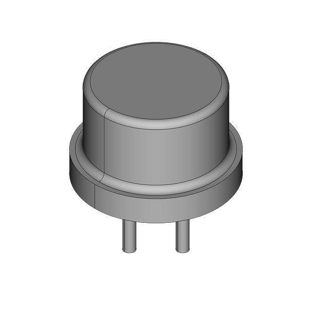
(TO-39)
Metal Can Package
20143830
CASE IS OUTPUT
Bottom View
See NS Package Number H03A
(TO-3)
Metal Can Package
20143829
CASE IS OUTPUT
Bottom View
See NS Package Number K02C
Ceramic SOIC
Chip Carrier
20143804
Top View
See NS Package Number WG16A
(Note 4)
LM117HV Series Packages
Part Number Suffix
Package
Design Load Current
H
T0–39
0.5A
K
TO-3
1.5A
WG, GW
Ceramic SOIC
0.5A
www.national.com
2
�20143808
LM117HVQML
Schematic Diagram
3
www.national.com
�LM117HVQML
Absolute Maximum Ratings (Note 1)
Power Dissipation (Note 2)
Input - Output Voltage Differential
Maximum Junction Temperature
Storage Temperature
Internally limited
+60V, −0.3V
+150°C
−65°C ≤ TA ≤ +150°C
300°C
Lead Temperature (Soldering, 10 sec.)
Thermal Resistance
θJA
T0-3 Metal Can - Still Air
T0-3 Metal Can - 500LF/Min Air flow
T0-39 Metal Can - Still Air
T0-39 Metal Can - 500LF/Min Air flow
Ceramic SOIC - Still Air “WG”
Ceramic SOIC - 500LF/Min Air flow “WG”
Ceramic SOIC - Still Air “GW”
Ceramic SOIC - 500LF/Min Air flow “GW”
39°C/W
14°C/W
186°C/W
64°C/W
115°C/W
66°C/W
130°C/W
80°C/W
θJC
T0-3 Metal Can
T0-39 Metal Can
Ceramic SOIC “WG” (Note 5)
Ceramic SOIC “GW”
ESD Tolerance (Note 3)
1.9°C/W
21°C/W
3.4°C/W
7°C/W
2000V
Recommended Operating Conditions
−55°C ≤ TA ≤ +125°C
Operating Temperature Range
Quality Conformance Inspection
Mil-Std-883, Method 5005 - Group A
Subgroup
Description
Temp °C
1
Static tests at
25
2
Static tests at
125
3
Static tests at
-55
4
Dynamic tests at
25
5
Dynamic tests at
125
6
Dynamic tests at
-55
7
Functional tests at
25
8A
Functional tests at
125
8B
Functional tests at
-55
9
Switching tests at
25
10
Switching tests at
125
11
Switching tests at
-55
12
Settling time at
25
13
Settling time at
125
14
Settling time at
-55
www.national.com
4
�DC Parameters
The following conditions apply, unless otherwise specified. VDiff = (VI − VO), IL = 8mA, VOUT = 1.25V (Nominal)
Symbol
IAdj
IQ
Parameter
Adjustment Pin Current
Minimum Load Current
Conditions
Notes
Min
Unit
VDiff = 3V
100
µA
1
VDiff = 3.3V
100
µA
2, 3
VDiff = 40V
100
µA
1, 2, 3
VDiff = 3V, VO = 1.7V
5.0
mA
1
VDiff = 3.3V, VO = 1.7V
5.0
mA
2, 3
VI = 40V, VO = 1.7V
5.0
mA
1, 2, 3
VI = 60V, VO = 1.7V
VRef
VRLine
VRLoad
Delta IAdj /
Load
8.2
mA
1
VDiff = 3V
1.2
1.3
V
1
VDiff = 3.3V
1.2
1.3
V
2, 3
VDiff = 40V
1.2
1.3
V
1, 2, 3
-8.64
8.64
mV
1
3.3V ≤ VDiff ≤ 40V,
VO = VRef
-18
18
mV
2, 3
40V ≤ VDiff ≤ 60V,
IL = 60mA
-25
25
mV
1
VDiff = 3V,
IL = 10mA to 500mA
-15
15
mV
1
VDiff = 3.3V,
IL = 10mA to 500mA
-15
15
mV
2, 3
VDiff = 40V,
IL = 10mA to 150mA
-15
15
mV
1
VDiff = 40V,
IL = 10mA to 100mA
-15
15
mV
2, 3
Adjustment Pin Current Change VDiff = 3V,
IL = 10mA to 500mA
-5.0
5.0
µA
1
VDiff = 3.3V,
IL = 10mA to 500mA
-5.0
5.0
µA
2, 3
VDiff = 40V,
IL = 10mA to 150mA
-5.0
5.0
µA
1
VDiff = 40V,
IL = 10mA to 100mA
-5.0
5.0
µA
2, 3
-5.0
5.0
µA
1
3.3V ≤ VDiff ≤ 40V
-5.0
5.0
µA
2, 3
VDiff = 60V
0.0
0.4
A
1
VDiff = 4.25V
0.5
1.8
A
1
6.0
mV
1
Reference Voltage
Line Regulation
Load Regulation
3V ≤ VDiff ≤ 40V,
VO = VRef
Delta IAdj /
Line
Adjustment Pin Current Change 3V ≤ VDiff ≤ 40V
IOS
Short Circuit Current
θR
Subgroups
Max
Thermal Regulation
VDiff = 40V, IL = 150mA,
t = 20mS
5
www.national.com
LM117HVQML
LM117HVH, HVWG Electrical Characteristics
�LM117HVQML
AC Parameters
The following conditions apply, unless otherwise specified. VDiff = (VI − VO), IL = 8mA, VOUT = 1.25V (Nominal)
Symbol
RR
Parameter
Ripple Rejection
Conditions
VI = +6.25V, ƒ = 120Hz,
eI = 1VRMS, IL = 125mA,
VO = VRef
Notes
Min
(Note 6)
66
Max
Unit
Subgroups
dB
4, 5, 6
LM117HVH, HVWG Delta Electrical Characteristics
DC Delta Parameters
The following conditions apply, unless otherwise specified.
Deltas performed on QMLV devices at Group B, Subgroup 5, only.
Symbol
Parameter
Conditions
IAdj
Adjust Pin Current
VRef
VRLine
Reference Voltage
Line Regulation
Notes
Min
Max
Unit
Subgroups
VDiff = 3V
-10
10
µA
1
VDiff = 40V
-10
10
µA
1
VDiff = 3V
-0.01
0.01
V
1
VDiff = 40V
-0.01
0.01
V
1
3V ≤ VDiff ≤ 40V,
VO = VRef
-4.0
4.0
mV
1
40V ≤ VDiff ≤ 60V,
IL = 60mA
-6.0
6.0
mV
1
LM117HVH, HVWG Post Radiation Electrical Characteristics
DC Parameters
The following conditions apply, unless otherwise specified. VDiff = (VI − VO), IL = 8mA, VOUT = 1.25V (Nominal)
Symbol
Parameter
Conditions
Notes
VDiff = 3V
Min
Max
Unit
Subgroups
1.2
1.45
V
1
VRef
Reference Voltage
VDiff = 40V
1.2
1.45
V
1
VRLine
Line Regulation
3V ≤ VDiff ≤ 40V,
VO = VRef
-40
40
mV
1
VRLoad
Load Regulation
VDiff = 3V,
IL = 10mA to 500mA
-27
27
mV
1
Unit
Subgroups
dB
4
AC Parameters
The following conditions apply, unless otherwise specified. VDiff = (VI − VO), IL = 8mA, VOUT = 1.25V (Nominal)
Symbol
RR
Parameter
Ripple Rejection
www.national.com
Conditions
VI = +6.25V, ƒ = 120Hz,
eI = 1VRMS, IL = 125mA,
VO = VRef
6
Notes
Min
55
Max
�DC Parameters
The following conditions apply, unless otherwise specified. VDiff =(VI − VO), IL = 10mA, VOUT = 1.25V (Nominal)
Symbol
IAdj
IQ
VRef
VRLine
VRLoad
Delta IAdj /
Load
Parameter
Adjustment Pin Current
Minimum Load Current
Conditions
Min
Subgroups
Max
Unit
VDiff = 3V
100
µA
1
VDiff = 3.3V
100
µA
2, 3
VDiff = 40V
100
µA
1, 2, 3
VDiff = 3V, VO = 1.7V
5.0
mA
1
VDiff = 3.3V, VO = 1.7V
5.0
mA
2, 3
VI = 40V, VO = 1.7V
5.0
mA
1, 2, 3
VI = 60V, VO = 1.7V
0.25
8.2
mA
1
VDiff = 3V
1.2
1.3
V
1
VDiff = 3.3V
1.2
1.3
V
2, 3
VDiff = 40V
1.2
1.3
V
1, 2, 3
-8.64
8.64
mV
1
3.3V ≤ VDiff ≤ 40V,
VO = VRef
-18
18
mV
2, 3
40V ≤ VDiff ≤ 60V,
IL = 60mA
-25
25
mV
1
VDiff = 3V,
IL = 10mA to 1.5A
-15
15
mV
1
VDiff = 3.3V,
IL = 10mA to 1.5A
-15
15
mV
2, 3
VDiff = 40V,
IL = 10mA to 300mA
-15
15
mV
1
VDiff = 40V,
IL = 10mA to 195mA
-15
15
mV
2, 3
Adjustment Pin Current Change VDiff = 3V,
IL = 10mA to 1.5A
-5.0
5.0
µA
1
VDiff = 3.3V,
IL = 10mA to 1.5A
-5.0
5.0
µA
2, 3
VDiff = 40V,
IL = 10mA to 300mA
-5.0
5.0
µA
1
VDiff = 40V,
IL = 10mA to 195mA
-5.0
5.0
µA
2, 3
-5.0
5.0
µA
1
3.3V ≤ VDiff ≤ 40V
-5.0
5.0
µA
2, 3
VDiff = 60V
0.0
0.4
A
1
VDiff = 3V
1.5
3.5
A
1
10.5
mV
1
Reference Voltage
Line Regulation
Load Regulation
3V ≤ VDiff ≤ 40V,
VO = VRef
Delta IAdj /
Line
Adjustment Pin Current Change 3V ≤ VDiff ≤ 40V
IOS
Short Circuit Current
θR
Notes
Thermal Regulation
VDiff = 40V, IL = 300mA,
t = 20mS
7
www.national.com
LM117HVQML
LM117HVK Electrical Characteristics
�LM117HVQML
AC Parameters
The following conditions apply, unless otherwise specified. VDiff = (VI − VO), IL = 10mA.
Symbol
RR
Parameter
Ripple Rejection
Conditions
VI = +6.25V, ƒ = 120Hz,
eI = 1VRMS, IL = 0.5A,
VO = VRef
Notes
Min
(Note 6)
66
Max
Unit
Subgroups
dB
4, 5, 6
Note 1: Absolute Maximum Ratings indicate limits beyond which damage to the device may occur. Operating Ratings indicate conditions for which the device is
functional, but do not guarantee specific performance limits. For guaranteed specifications and test conditions, see the Electrical Characteristics. The guaranteed
specifications apply only for the test conditions listed. Some performance characteristics may degrade when the device is not operated under the listed test
conditions.
Note 2: The maximum power dissipation must be derated at elevated temperatures and is dictated by TJmax (maximum junction temperature), θJA (package
junction to ambient thermal resistance), and TA (ambient temperature). The maximum allowable power dissipation at any temperature is PDmax = (TJmax - TA) /
θJA or the number given in the Absolute Maximum Ratings, whichever is lower. "Although power dissipation is internally limited, these specifications are applicable
for power dissipations of 2W for the TO39 package and 20W for the TO3 package."
Note 3: Human body model, 1.5 kΩ in series with 100 pF.
Note 4: For the Ceramic SOIC device to function properly, the “Output” and “Output/Sense” pins must be connected on the users printed circuit board.
Note 5: The package material for these devices allows much improved heat transfer over our standard ceramic packages. In order to take full advantage of this
improved heat transfer, heat sinking must be provided between the package base (directly beneath the die), and either metal traces on, or thermal vias through,
the printed circuit board. Without this additional heat sinking, device power dissipation must be calculated using θJA, rather than θJC, thermal resistance. It must
not be assumed that the device leads will provide substantial heat transfer out the package, since the thermal resistance of the lead frame material is very poor,
relative to the material of the package base. The stated θJC thermal resistance is for the package material only, and does not account for the additional thermal
resistance between the package base and the printed circuit board. The user must determine the value of the additional thermal resistance and must combine
this with the stated value for the package, to calculate the total allowed power dissipation for the device.
Note 6: Tested @ 25°C; guaranteed, but not tested @ 125°C & −55°C
Note 7: Pre and post irradiation limits are identical to those listed under AC and DC electrical characteristics, except as listed in the “LM117HVH, HVWG Post
Radiation Electrical Characteristics” tables . These parts may be dose rate sensitive in a space environment and demonstrate enhanced low dose rate effect.
Radiation end point limits for the noted parameters are guaranteed only for the conditions as specified in Mil-Std-883, Method 1019, Condition A.
Note 8: Pre and post irradiation limits are identical to those listed under AC and DC electrical characteristics, except as listed in the “LM117HVH, HVWG Post
Radiation Electrical Characteristics” tables. These parts pass all post irradiation limits under low dose rate testing at 10 mrad(Si)/s. Low dose rate qualification is
performed on a wafer-by-wafer basis, per test method 1019 condition E of MIL-STD-883.
www.national.com
8
�LM117HVQML
Typical Performance Characteristics
Output capacitor = 0 μF unless otherwise noted.
Load Regulation
Current Limit
20143832
20143833
Adjustment Current
Dropout Voltage
20143835
20143834
Temperature Stability
Minimum Operating Current
20143836
20143837
9
www.national.com
�LM117HVQML
Ripple Rejection
Ripple Rejection
20143838
20143839
Ripple Rejection
Output Impedance
20143840
20143841
Line Transient Response
Load Transient Response
20143842
www.national.com
20143843
10
�LM117HVQML
Typical Radiation Characteristics
(Note 9)
Reference Voltage
Load Regulation
20143848
20143849
Line Regulation
Ripple Rejection
20143850
20143851
Note 9: Irradiation conditions: VI = 60V; low dose rate = 10 mrad(Si)/s
11
www.national.com
�LM117HVQML
tance can cause excessive ringing. This occurs with values
between 500 pF and 5000 pF. A 1 μF solid tantalum (or 25
μF aluminum electrolytic) on the output swamps this effect
and insures stability. Any increase of load capacitance larger
than 10 μF will merely improve the loop stability and output
impedance.
Application Hints
In operation, the LM117HV develops a nominal 1.25V reference voltage, VREF, between the output and adjustment terminal. The reference voltage is impressed across program
resistor R1 and, since the voltage is constant, a constant current I1 then flows through the output set resistor R2, giving an
output voltage of
LOAD REGULATION
The LM117HV is capable of providing extremely good load
regulation but a few precautions are needed to obtain maximum performance. The current set resistor connected between the adjustment terminal and the output terminal
(usually 240Ω) should be tied directly to the output of the regulator rather than near the load. This eliminates line drops
from appearing effectively in series with the reference and
degrading regulation. For example, a 15V regulator with
0.05Ω resistance between the regulator and load will have a
load regulation due to line resistance of 0.05Ω × IL. If the set
resistor is connected near the load the effective line resistance will be 0.05Ω (1 + R2/R1) or in this case, 11.5 times
worse.
Figure 2 shows the effect of resistance between the regulator
and 240Ω set resistor.
20143805
FIGURE 1.
Since the 100 μA current from the adjustment terminal represents an error term, the LM117HV was designed to minimize IADJ and make it very constant with line and load
changes. To do this, all quiescent operating current is returned to the output establishing a minimum load current
requirement. If there is insufficient load on the output, the output will rise.
20143806
FIGURE 2. Regulator with Line
Resistance in Output Lead
EXTERNAL CAPACITORS
An input bypass capacitor is recommended. A 0.1 μF disc or
1 μF solid tantalum on the input is suitable input bypassing for
almost all applications. The device is more sensitive to the
absence of input bypassing when adjustment or output capacitors are used but the above values will eliminate the
possibility of problems.
The adjustment terminal can be bypassed to ground on the
LM117HV to improve ripple rejection. This bypass capacitor
prevents ripple from being amplified as the output voltage is
increased. With a 10 μF bypass capacitor 80 dB ripple rejection is obtainable at any output level. Increases over 10 μF do
not appreciably improve the ripple rejection at frequencies
above 120 Hz. If the bypass capacitor is used, it is sometimes
necessary to include protection diodes to prevent the capacitor from discharging through internal low current paths and
damaging the device.
In general, the best type of capacitors to use are solid tantalum. Solid tantalum capacitors have low impedance even at
high frequencies. Depending upon capacitor construction, it
takes about 25 μF in aluminum electrolytic to equal 1 μF solid
tantalum at high frequencies. Ceramic capacitors are also
good at high frequencies; but some types have a large decrease in capacitance at frequencies around 0.5 MHz. For this
reason, 0.01 μF disc may seem to work better than a 0.1 μF
disc as a bypass.
Although the LM117HV is stable with no output capacitors,
like any feedback circuit, certain values of external capaciwww.national.com
With the TO-3 package, it is easy to minimize the resistance
from the case to the set resistor, by using two separate leads
to the case. However, with the TO-5 package, care should be
taken to minimize the wire length of the output lead. The
ground of R2 can be returned near the ground of the load to
provide remote ground sensing and improve load regulation.
PROTECTION DIODES
When external capacitors are used with any IC regulator it is
sometimes necessary to add protection diodes to prevent the
capacitors from discharging through low current points into
the regulator. Most 10 μF capacitors have low enough internal
series resistance to deliver 20A spikes when shorted. Although the surge is short, there is enough energy to damage
parts of the IC.
When an output capacitor is connected to a regulator and the
input is shorted, the output capacitor will discharge into the
output of the regulator. The discharge current depends on the
value of the capacitor, the output voltage of the regulator, and
the rate of decrease of VIN. In the LM117HV, this discharge
path is through a large junction that is able to sustain 15A
surge with no problem. This is not true of other types of positive regulators. For output capacitors of 25 μF or less, there
is no need to use diodes.
The bypass capacitor on the adjustment terminal can discharge through a low current junction. Discharge occurs when
12
�LM117HVQML
either the input or output is shorted. Internal to the LM117HV
is a 50Ω resistor which limits the peak discharge current. No
protection is needed for output voltages of 25V or less and 10
μF capacitance. Figure 3 shows an LM117HV with protection
diodes included for use with outputs greater than 25V and
high values of output capacitance.
Note: D1 protects against C1
D2 protects against C2
CURRENT LIMIT
Internal current limit will be activated whenever the output
current exceeds the limit indicated in the Typical Performance
Characteristics. However, if during a short circuit condition the
regulator's differential voltage exceeds the Absolute Maximum Rating of 60V (e.g. VIN ≥ 60V, VOUT = 0V), internal
junctions in the regulator may break down and the device may
be damaged or fail. Failure modes range from an apparent
open or short from input to output of the regulator, to a destroyed package (most common with the TO-220 package).
To protect the regulator, the user is advised to be aware of
voltages that may be applied to the regulator during fault conditions, and to avoid violating the Absolute Maximum Ratings.
20143807
FIGURE 3. Regulator with Protection Diodes
13
www.national.com
�LM117HVQML
Typical Applications
1.2V-45V Adjustable Regulator
20143801
Full output current not available at high input-output voltages
†Optional—improves transient response. Output capacitors in the range of 1 μF to 1000 μF of aluminum or tantalum electrolytic
are commonly used to provide improved output impedance and rejection of transients.
*Needed if device is more than 6 inches from filter capacitors.
Digitally Selected Outputs
5V Logic Regulator with
Electronic Shutdown*
*Min. output ≈ 1.2V
20143803
20143802
*Sets maximum VOUT
Slow Turn-On 15V Regulator
Adjustable Regulator with Improved
Ripple Rejection
20143810
20143809
†Solid tantalum
*Discharges C1 if output is shorted to ground
www.national.com
14
�LM117HVQML
High Stability 10V Regulator
High Current Adjustable Regulator
20143811
20143812
†Solid tantalum
*Minimum load current = 30 mA
‡Optional—improves ripple rejection
0 to 30V Regulator
Power Follower
20143813
20143814
Full output current not available at high input-output voltages
15
www.national.com
�LM117HVQML
5A Constant Voltage/Constant Current Regulator
20143815
†Solid tantalum
*Lights in constant current mode
1A Current Regulator
1.2V–20V Regulator with
Minimum Program Current
20143816
*Minimum load current ≈ 4 mA
www.national.com
16
20143817
�LM117HVQML
High Gain Amplifier
Low Cost 3A Switching Regulator
20143819
20143818
†Solid tantalum
*Core—Arnold A-254168-2 60 turns
4A Switching Regulator with Overload Protection
20143820
†Solid tantalum
*Core—Arnold A-254168-2 60 turns
Precision Current Limiter
20143821
* 0.8Ω ≤ R1 ≤ 120Ω
17
www.national.com
�LM117HVQML
Tracking Preregulator
20143822
Adjustable Multiple On-Card Regulators
with Single Control*
20143823
*All outputs within ±100 mV
†Minimum load—10 mA
AC Voltage Regulator
12V Battery Charger
20143825
20143824
www.national.com
Use of RS allows low charging rates with fully charged battery.
**The 1000 μF is recommended to filter out input transients
18
�LM117HVQML
50 mA Constant Current Battery Charger
20143826
Adjustable 4A Regulator
Current Limited 6V Charger
20143828
*Sets peak current (0.6A for 1Ω)
**The 1000 μF is recommended to filter out input transients
20143827
19
www.national.com
�LM117HVQML
Revision History
Date Released Revision
03/14/06
Section
Originator
New Release, Corporate format
07/06/07
B
Features, Ordering Information,
Connection Diagram, Absolute
Maximum Ratings, Electrical's, Notes
and Physical Dimensions
Larry McGee Added Radiation information and WG
information to data sheet. Revision A to be
Archived.
02/13/08
C
Features, Ordering Information,
Electrical's, Notes and Typical
Radiation Characteristics, Physical
Dimensions Drawing
Larry McGee Added ELDRS NSID information, HVH &
HVWG Delta and Post Radiation Table,
Typical Radiation Characteristics Plots, Note
8, 9 and WG Market Drawing. Revision B to be
Archived.
09/02/11
D
Ordering Information, Absolute
Maximum Ratings
Larry McGee Added 'GW' NSIDS & SMD numbers. Added
Theta JA and Theta JC for 'GW' devices.
Revision C to be Archived.
www.national.com
L. Lytle
Changes
A
20
2 MDS datasheets converted into one
Corporate datasheet format. Corrected IL from
60mA to 8mA for RLine. Separated Delta IAdj /
Line from Delta IAdj / Load for both the H & K
devices. Removed drift from MNLM117HV-H
electrical characteristics since not performed
on 883 product. MNLM117HV-K Rev 0C1 &
MNLM117HV-H Rev 2A1 will be archived.
�LM117HVQML
Physical Dimensions inches (millimeters) unless otherwise noted
T0-39 Metal Can Package (H)
NS Package Number H03A
T0-3 Metal Can Package (K)
NS Package Number K02C
21
www.national.com
�LM117HVQML
Ceramic SOIC
NS Package Number WG16A
www.national.com
22
�LM117HVQML
23
www.national.com
�LM117HVQML 3-Terminal Adjustable Regulator
Notes
For more National Semiconductor product information and proven design tools, visit the following Web sites at:
www.national.com
Products
Design Support
Amplifiers
www.national.com/amplifiers
WEBENCH® Tools
www.national.com/webench
Audio
www.national.com/audio
App Notes
www.national.com/appnotes
Clock and Timing
www.national.com/timing
Reference Designs
www.national.com/refdesigns
Data Converters
www.national.com/adc
Samples
www.national.com/samples
Interface
www.national.com/interface
Eval Boards
www.national.com/evalboards
LVDS
www.national.com/lvds
Packaging
www.national.com/packaging
Power Management
www.national.com/power
Green Compliance
www.national.com/quality/green
Switching Regulators
www.national.com/switchers
Distributors
www.national.com/contacts
LDOs
www.national.com/ldo
Quality and Reliability
www.national.com/quality
LED Lighting
www.national.com/led
Feedback/Support
www.national.com/feedback
Voltage References
www.national.com/vref
Design Made Easy
www.national.com/easy
www.national.com/powerwise
Applications & Markets
www.national.com/solutions
Mil/Aero
www.national.com/milaero
PowerWise® Solutions
Serial Digital Interface (SDI) www.national.com/sdi
Temperature Sensors
www.national.com/tempsensors SolarMagic™
www.national.com/solarmagic
PLL/VCO
www.national.com/wireless
www.national.com/training
PowerWise® Design
University
THE CONTENTS OF THIS DOCUMENT ARE PROVIDED IN CONNECTION WITH NATIONAL SEMICONDUCTOR CORPORATION
(“NATIONAL”) PRODUCTS. NATIONAL MAKES NO REPRESENTATIONS OR WARRANTIES WITH RESPECT TO THE ACCURACY
OR COMPLETENESS OF THE CONTENTS OF THIS PUBLICATION AND RESERVES THE RIGHT TO MAKE CHANGES TO
SPECIFICATIONS AND PRODUCT DESCRIPTIONS AT ANY TIME WITHOUT NOTICE. NO LICENSE, WHETHER EXPRESS,
IMPLIED, ARISING BY ESTOPPEL OR OTHERWISE, TO ANY INTELLECTUAL PROPERTY RIGHTS IS GRANTED BY THIS
DOCUMENT.
TESTING AND OTHER QUALITY CONTROLS ARE USED TO THE EXTENT NATIONAL DEEMS NECESSARY TO SUPPORT
NATIONAL’S PRODUCT WARRANTY. EXCEPT WHERE MANDATED BY GOVERNMENT REQUIREMENTS, TESTING OF ALL
PARAMETERS OF EACH PRODUCT IS NOT NECESSARILY PERFORMED. NATIONAL ASSUMES NO LIABILITY FOR
APPLICATIONS ASSISTANCE OR BUYER PRODUCT DESIGN. BUYERS ARE RESPONSIBLE FOR THEIR PRODUCTS AND
APPLICATIONS USING NATIONAL COMPONENTS. PRIOR TO USING OR DISTRIBUTING ANY PRODUCTS THAT INCLUDE
NATIONAL COMPONENTS, BUYERS SHOULD PROVIDE ADEQUATE DESIGN, TESTING AND OPERATING SAFEGUARDS.
EXCEPT AS PROVIDED IN NATIONAL’S TERMS AND CONDITIONS OF SALE FOR SUCH PRODUCTS, NATIONAL ASSUMES NO
LIABILITY WHATSOEVER, AND NATIONAL DISCLAIMS ANY EXPRESS OR IMPLIED WARRANTY RELATING TO THE SALE
AND/OR USE OF NATIONAL PRODUCTS INCLUDING LIABILITY OR WARRANTIES RELATING TO FITNESS FOR A PARTICULAR
PURPOSE, MERCHANTABILITY, OR INFRINGEMENT OF ANY PATENT, COPYRIGHT OR OTHER INTELLECTUAL PROPERTY
RIGHT.
LIFE SUPPORT POLICY
NATIONAL’S PRODUCTS ARE NOT AUTHORIZED FOR USE AS CRITICAL COMPONENTS IN LIFE SUPPORT DEVICES OR
SYSTEMS WITHOUT THE EXPRESS PRIOR WRITTEN APPROVAL OF THE CHIEF EXECUTIVE OFFICER AND GENERAL
COUNSEL OF NATIONAL SEMICONDUCTOR CORPORATION. As used herein:
Life support devices or systems are devices which (a) are intended for surgical implant into the body, or (b) support or sustain life and
whose failure to perform when properly used in accordance with instructions for use provided in the labeling can be reasonably expected
to result in a significant injury to the user. A critical component is any component in a life support device or system whose failure to perform
can be reasonably expected to cause the failure of the life support device or system or to affect its safety or effectiveness.
National Semiconductor and the National Semiconductor logo are registered trademarks of National Semiconductor Corporation. All other
brand or product names may be trademarks or registered trademarks of their respective holders.
Copyright© 2011 National Semiconductor Corporation
For the most current product information visit us at www.national.com
National Semiconductor
Americas Technical
Support Center
Email: support@nsc.com
Tel: 1-800-272-9959
www.national.com
National Semiconductor Europe
Technical Support Center
Email: europe.support@nsc.com
National Semiconductor Asia
Pacific Technical Support Center
Email: ap.support@nsc.com
National Semiconductor Japan
Technical Support Center
Email: jpn.feedback@nsc.com
�


 工商网监
湘ICP备2023018690号
工商网监
湘ICP备2023018690号

