LM118QML
www.ti.com
SNOSAJ3A – JULY 2005 – REVISED MARCH 2013
LM118QML Operational Amplifier
Check for Samples: LM118QML
FEATURES
DESCRIPTION
•
•
•
•
•
•
•
The LM118 is a precision high speed operational
amplifier designed for applications requiring wide
bandwidth and high slew rate. It features a factor of
ten increase in speed over general purpose devices
without sacrificing DC performance.
1
2
15 MHz Small Signal Bandwidth
Ensured 50V/μs Slew Rate
Maximum Bias Current of 250 nA
Operates from Supplies of ±5V to ±20V
Internal Frequency Compensation
Input and Output Overload Protected
Pin Compatible with General Purpose Op
Amps
The LM118 has internal unity gain frequency
compensation. This considerably simplifies its
application since no external components are
necessary for operation. However, unlike most
internally compensated amplifiers, external frequency
compensation may be added for optimum
performance. For inverting applications, feed forward
compensation will boost the slew rate to over
150V/μs and almost double the bandwidth.
Overcompensation can be used with the amplifier for
greater stability when maximum bandwidth is not
needed. Further, a single capacitor can be added to
reduce the 0.1% settling time to under 1 μs.
The high speed and fast settling time of this op amp
makes it useful in A/D converters, oscillators, active
filters, sample and hold circuits, or general purpose
amplifiers. This device is easy to apply and offers an
order of magnitude better AC performance than
industry standards such as the LM709.
Fast Voltage Follower
Do not hard-wire as voltage follower (R1 ≥ 5 kΩ)
1
2
Please be aware that an important notice concerning availability, standard warranty, and use in critical applications of
Texas Instruments semiconductor products and disclaimers thereto appears at the end of this data sheet.
All trademarks are the property of their respective owners.
PRODUCTION DATA information is current as of publication date.
Products conform to specifications per the terms of the Texas
Instruments standard warranty. Production processing does not
necessarily include testing of all parameters.
Copyright © 2005–2013, Texas Instruments Incorporated
�LM118QML
SNOSAJ3A – JULY 2005 – REVISED MARCH 2013
www.ti.com
These devices have limited built-in ESD protection. The leads should be shorted together or the device placed in conductive foam
during storage or handling to prevent electrostatic damage to the MOS gates.
Connection Diagram
Figure 1. CDIP Package
Top View
See Package Number J0014A
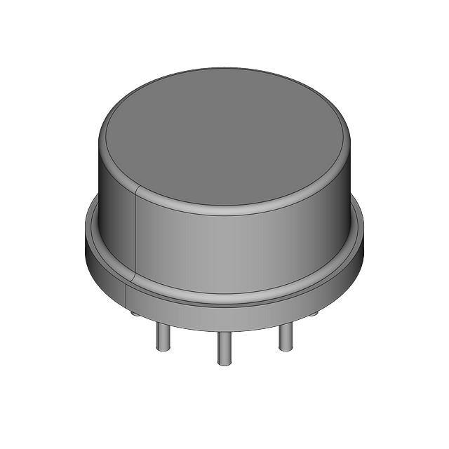
Figure 2. TO-99
Top View
See Package Number LMC
N/C
1
10
Bal/Comp1
2
9
Comp2
-IN
3
8
V+
+IN
4
7
OUT
V-
5
6
Bal/Comp3
N/C
Pin connections shown on schematic diagram and typical
applications are for TO package.
Figure 3. CDIP Package
Top View
See Package Number NAB0008A
2
Figure 4. CLGA Package
Top View
See NS Package Number NAC0010A
Submit Documentation Feedback
Copyright © 2005–2013, Texas Instruments Incorporated
Product Folder Links: LM118QML
�LM118QML
www.ti.com
SNOSAJ3A – JULY 2005 – REVISED MARCH 2013
Schematic Diagram
Submit Documentation Feedback
Copyright © 2005–2013, Texas Instruments Incorporated
Product Folder Links: LM118QML
3
�LM118QML
SNOSAJ3A – JULY 2005 – REVISED MARCH 2013
www.ti.com
Absolute Maximum Ratings (1)
Supply Voltage
Power Dissipation (2)
±20V
8 LD TO-99
750mW
8LD CDIP
1000mW
14LD CDIP
1250mW
10LD CLGA
600mW
Differential Input Current (3)
±10 mA
Input Voltage (4)
±15V
Output Short-Circuit Duration
Continuous
−55°C ≤ TA ≤ +125°C
Operating Temperature Range
Thermal Resistance
8 LD TO-99 (Still Air @ 0.5W)
θJA
θJC
160°C/W
8 LD TO-99 (500LF / Min Air flow @ 0.5W)
86°C/W
8LD CDIP (Still Air @ 0.5W)
120°C/W
8LD CDIP (500LF / Min Air flow @ 0.5W)
66°C/W
14LD CDIP (Still Air @ 0.5W)
87°C/W
14LD CDIP (500LF / Min Air flow @ 0.5W)
51°C/W
10LD CLGA (Still Air @ 0.5W)
198°C/W
10LD CLGA (500LF / Min Air flow @ 0.5W)
124°C/W
8 LD TO-99
48°C/W
8LD CDIP
17°C/W
14LD CDIP
17°C/W
10LD CLGA
22°C/W
−65°C ≤ TA ≤ +150°C
Storage Temperature Range
Lead Temperature (Soldering, 10 seconds)
300°C
ESD Tolerance (5)
2000V
(1)
(2)
(3)
(4)
(5)
4
Absolute Maximum Ratings indicate limits beyond which damage to the device may occur. Operating Ratings indicate conditions for
which the device is functional, but do not ensure specific performance limits. For specifications and test conditions, see the Electrical
Characteristics. The specifications apply only for the test conditions listed. Some performance characteristics may degrade when the
device is not operated under the listed test conditions.
The maximum power dissipation must be derated at elevated temperatures and is dictated by TJmax (maximum junction temperature),
θJA (package junction to ambient thermal resistance), and TA (ambient temperature). The maximum allowable power dissipation at any
temperature is PDmax = (TJmax - TA)/θJA or the number given in the Absolute Maximum Ratings, whichever is lower.
The inputs are shunted with back-to-back diodes for over voltage protection. Therefore, excessive current will flow if a differential input
voltage in excess of 1V is applied between the inputs unless some limiting resistance is used.
For supply voltages less than ±15V, the absolute maximum input voltage is equal to the supply voltage.
Human body model, 1.5 kΩ in series with 100 pF.
Submit Documentation Feedback
Copyright © 2005–2013, Texas Instruments Incorporated
Product Folder Links: LM118QML
�LM118QML
www.ti.com
SNOSAJ3A – JULY 2005 – REVISED MARCH 2013
Quality Conformance Inspection
Mil-Std-883, Method 5005; Group A
Subgroup
Description
Temp°C
1
Static tests at
25
2
Static tests at
125
3
Static tests at
-55
4
Dynamic tests at
25
5
Dynamic tests at
125
6
Dynamic tests at
-55
7
Functional tests at
25
8A
Functional tests at
125
8B
Functional tests at
-55
9
Switching tests at
25
10
Switching tests at
125
11
Switching tests at
-55
12
Settling time at
25
13
Settling time at
125
14
Settling time at
-55
LM118/883 Electrical Characteristics DC Parameters
The following conditions apply, unless otherwise specified.
DC VCC = ±15V, VCM = 0V
Symbol
VIO
Parameter
Input Offset Voltage
Conditions
VCM = ± 11.5V, RS = 50Ω
VCC = ± 20V, RS = 50Ω
IIO
Input Offset Current
-4.0
+4.0
mV
1
-6.0
+6.0
mV
2, 3
-4.0
+4.0
mV
1
2, 3
+6.0
mV
+4.0
mV
1
-6.0
+6.0
mV
2, 3
VCC = ± 5V, RS = 50Ω
-4.0
+4.0
mV
1
-6.0
+6.0
mV
2, 3
-50
+50
nA
1
-100
+100
nA
2, 3
VCM = ± 11.5V, RS = 10KΩ
VCM = ± 11.5V, RS= 10KΩ
VCC = ± 5V, RS = 10KΩ
Power Supply Rejection Ratio
Unit
-4.0
VCC = ± 20V, RS = 10KΩ
PSRR
Max
-6.0
VCC = ± 5V, RS = 10KΩ
Input Bias Current
Subgroups
Min
VCC = ± 20V, VCM = ± 15V,
RS = 50Ω
VCC = ± 20V, RS = 10KΩ
IIB
Notes
-50
+50
nA
1
-100
+100
nA
2, 3
-50
+50
nA
1
-100
+100
nA
2, 3
1.0
250
nA
1
1.0
500
nA
2, 3
1.0
250
nA
1
1.0
500
nA
2, 3
1.0
250
nA
1
1.0
500
nA
2, 3
+VCC = 20V to 5V, RS = 50Ω
70
dB
1, 2, 3
-VCC = -20V to -5V, RS = 50Ω
70
dB
1, 2, 3
dB
1, 2, 3
mA
1, 2, 3
CMRR
Common Mode Rejection Ratio
VCC = ± 15V, VCM = ± 11.5V, RS =
50Ω
80
+IOS
Short Circuit Current
t < 25mS
-65
-5.0
Submit Documentation Feedback
Copyright © 2005–2013, Texas Instruments Incorporated
Product Folder Links: LM118QML
5
�LM118QML
SNOSAJ3A – JULY 2005 – REVISED MARCH 2013
www.ti.com
LM118/883 Electrical Characteristics DC Parameters (continued)
The following conditions apply, unless otherwise specified.
DC VCC = ±15V, VCM = 0V
Symbol
-IOS
Parameter
Short Circuit Current
ICC
Power Supply Current
VIO adj.
Input Offset Voltage Adjust
RI
Input Resistance
VI
Input Voltage Range
AVS
Large Signal Voltage Gain
Conditions
t < 25mS
(1)
(2)
(3)
Output Voltage Swing
Min
Max
Unit
Subgroups
5.0
65
mA
1, 2
5.0
80
mA
3
8.0
mA
1
7.0
mA
2
11
mA
3
-4.0
mV
1
MΩ
1
V
1, 2, 3
VCC = ± 20V
VCC = ± 20V
VCC = ± 15V
RL = 2KΩ, VO = 0 to -10V
RL = 2KΩ, VO = 0 to +10V
VO
Notes
4.0
See (1)
1.0
See (2)
-11.5
+11.
5
(3)
50
V/mV
4
See (3)
25
V/mV
5, 6
See (3)
50
V/mV
4
See (3)
25
V/mV
5, 6
See
RL= 2KΩ
+12
-12
V
4, 5, 6
Min
Max
Unit
Subgroups
Specified by design not tested
Specified by CMRR
Datalog in K = V/mV
LM118/883 Electrical Characteristics AC Parameters
The following conditions apply parameters, unless otherwise specified.
AC VCC = ±15V, VCM = 0V, RS = 0Ω, RL = 2KΩ,, CL = 33pF
Symbol
SR
6
Parameter
Slew Rate
Conditions
Notes
VCC = ± 20V, VI = -5V to +5V, AV=1
50
V/µS
7
VCC = ± 20V, VI = +5V to -5V, AV=1
50
V/µS
7
Submit Documentation Feedback
Copyright © 2005–2013, Texas Instruments Incorporated
Product Folder Links: LM118QML
�LM118QML
www.ti.com
SNOSAJ3A – JULY 2005 – REVISED MARCH 2013
Typical Performance Characteristics
Input Current
Voltage Gain
Figure 5.
Figure 6.
Power Supply Rejection
Input Noise Voltage
Figure 7.
Figure 8.
Common Mode Rejection
Supply Current
Figure 9.
Figure 10.
Submit Documentation Feedback
Copyright © 2005–2013, Texas Instruments Incorporated
Product Folder Links: LM118QML
7
�LM118QML
SNOSAJ3A – JULY 2005 – REVISED MARCH 2013
www.ti.com
Typical Performance Characteristics (continued)
8
Closed Loop Output Impedance
Current Limiting
Figure 11.
Figure 12.
Input Current
Unity Gain Bandwidth
Figure 13.
Figure 14.
Voltage Follower Slew Rate
Inverter Settling Time
Figure 15.
Figure 16.
Submit Documentation Feedback
Copyright © 2005–2013, Texas Instruments Incorporated
Product Folder Links: LM118QML
�LM118QML
www.ti.com
SNOSAJ3A – JULY 2005 – REVISED MARCH 2013
Typical Performance Characteristics (continued)
Large Signal Frequency Response
Open Loop Frequency Response
Figure 17.
Figure 18.
Voltage Follower Pulse Response
Large Signal Frequency Response
Figure 19.
Figure 20.
Open Loop Frequency Response
Inverter Pulse Response
Figure 21.
Figure 22.
Submit Documentation Feedback
Copyright © 2005–2013, Texas Instruments Incorporated
Product Folder Links: LM118QML
9
�LM118QML
SNOSAJ3A – JULY 2005 – REVISED MARCH 2013
www.ti.com
AUXILIARY CIRCUITS
Feedforward Compensation
for Greater Inverting Slew Rate
Compensation for Minimum Settling Time
Slew and settling time to 0.1% for a 10V step change is 800 ns.
Slew rate typically 150V/μs.
Offset Balancing
Isolating Large Capacitive Loads
Overcompensation
10
Submit Documentation Feedback
Copyright © 2005–2013, Texas Instruments Incorporated
Product Folder Links: LM118QML
�LM118QML
www.ti.com
SNOSAJ3A – JULY 2005 – REVISED MARCH 2013
Typical Applications
Fast Voltage Follower
Do not hard-wire as voltage follower (R1 ≥ 5 kΩ)
Integrator or Slow Inverter
CF = Large (CF ≥ 50 pF)
*Do not hard-wire as integrator or slow inverter; insert a 10k-5 pF network in series with the input, to prevent
oscillation.
Fast Summing Amplifier
Differential Amplifier
Submit Documentation Feedback
Copyright © 2005–2013, Texas Instruments Incorporated
Product Folder Links: LM118QML
11
�LM118QML
SNOSAJ3A – JULY 2005 – REVISED MARCH 2013
www.ti.com
Fast Sample and Hold
D/A Converter Using Ladder Network
*Optional—Reduces settling time.
12
Submit Documentation Feedback
Copyright © 2005–2013, Texas Instruments Incorporated
Product Folder Links: LM118QML
�LM118QML
www.ti.com
SNOSAJ3A – JULY 2005 – REVISED MARCH 2013
Four Quadrant Multiplier
ΔOutput zero.
*“Y” zero
+“X” zero
‡Full scale adjust.
D/A Converter Using Binary Weighted Network
*Optional—Reduces settling time.
Submit Documentation Feedback
Copyright © 2005–2013, Texas Instruments Incorporated
Product Folder Links: LM118QML
13
�LM118QML
SNOSAJ3A – JULY 2005 – REVISED MARCH 2013
www.ti.com
Fast Summing Amplifier with Low Input Current
Wein Bridge Sine Wave Oscillator
14
Submit Documentation Feedback
Instrumentation Amplifier
Copyright © 2005–2013, Texas Instruments Incorporated
Product Folder Links: LM118QML
�LM118QML
www.ti.com
SNOSAJ3A – JULY 2005 – REVISED MARCH 2013
REVISION HISTORY SECTION
Date Released
Revision
Section
07/12/05
A
New Release, Corporate format
03/20/2013
A
All Sections
Originator
L. Lytle
Changes
1 MDS data sheet, MNLM118–X Rev 0A0 was
converted into the Corp. datasheet format.
MDS datasheet will be archived.
Changed Layout of National Data Sheet to TI
format
Submit Documentation Feedback
Copyright © 2005–2013, Texas Instruments Incorporated
Product Folder Links: LM118QML
15
�PACKAGE OPTION ADDENDUM
www.ti.com
14-Jan-2019
PACKAGING INFORMATION
Orderable Device
Status
(1)
Package Type Package Pins Package
Drawing
Qty
Eco Plan
Lead/Ball Finish
MSL Peak Temp
(2)
(6)
(3)
Op Temp (°C)
Device Marking
(4/5)
LM118 MD8
ACTIVE
DIESALE
Y
0
182
Green (RoHS
& no Sb/Br)
Call TI
Level-1-NA-UNLIM
-55 to 125
LM118H/883
ACTIVE
TO-99
LMC
8
20
TBD
Call TI
Call TI
-55 to 125
LM118H/883 Q ACO
LM118H/883 Q >T
LM118J-8/883
ACTIVE
CDIP
NAB
8
40
TBD
Call TI
Call TI
-55 to 125
LM118J-8
/883 Q ACO
/883 Q >T
(1)
The marketing status values are defined as follows:
ACTIVE: Product device recommended for new designs.
LIFEBUY: TI has announced that the device will be discontinued, and a lifetime-buy period is in effect.
NRND: Not recommended for new designs. Device is in production to support existing customers, but TI does not recommend using this part in a new design.
PREVIEW: Device has been announced but is not in production. Samples may or may not be available.
OBSOLETE: TI has discontinued the production of the device.
(2)
RoHS: TI defines "RoHS" to mean semiconductor products that are compliant with the current EU RoHS requirements for all 10 RoHS substances, including the requirement that RoHS substance
do not exceed 0.1% by weight in homogeneous materials. Where designed to be soldered at high temperatures, "RoHS" products are suitable for use in specified lead-free processes. TI may
reference these types of products as "Pb-Free".
RoHS Exempt: TI defines "RoHS Exempt" to mean products that contain lead but are compliant with EU RoHS pursuant to a specific EU RoHS exemption.
Green: TI defines "Green" to mean the content of Chlorine (Cl) and Bromine (Br) based flame retardants meet JS709B low halogen requirements of