LM19
www.ti.com
SNIS122E – MAY 2001 – REVISED MARCH 2013
LM19 2.4V, 10µA, TO-92 Temperature Sensor
Check for Samples: LM19
FEATURES
1
•
•
•
•
•
2
Rated for Full −55°C to +130°C Range
Available in a TO-92 Package
Predictable Curvature Error
Suitable for Remote Applications
UL Recognized Component
APPLICATIONS
•
•
•
•
•
•
•
•
•
Cellular Phones
Computers
Power Supply Modules
Battery Management
FAX Machines
Printers
HVAC
Disk Drives
Appliances
KEY SPECIFICATIONS
•
•
•
•
•
•
•
Accuracy at +30°C ±2.5 °C (max)
Accuracy at +130°C & −55°C ±3.5 to ±3.8 °C
(max)
Power Supply Voltage Range +2.4V to +5.5V
Current Drain 10 μA (max)
Nonlinearity ±0.4 % (typ)
Output Impedance 160 Ω (max)
Load Regulation
– 0µA < IL< +16 µA
DESCRIPTION
The LM19 is a precision analog output CMOS
integrated-circuit temperature sensor that operates
over a −55°C to +130°C temperature range. The
power supply operating range is +2.4 V to +5.5 V.
The transfer function of LM19 is predominately linear,
yet has a slight predictable parabolic curvature. The
accuracy of the LM19 when specified to a parabolic
transfer function is ±2.5°C at an ambient temperature
of +30°C. The temperature error increases linearly
and reaches a maximum of ±3.8°C at the
temperature range extremes. The temperature range
is affected by the power supply voltage. At a power
supply voltage of 2.7 V to 5.5 V the temperature
range extremes are +130°C and −55°C. Decreasing
the power supply voltage to 2.4 V changes the
negative extreme to −30°C, while the positive
remains at +130°C.
The LM19's quiescent current is less than 10 μA.
Therefore, self-heating is less than 0.02°C in still air.
Shutdown capability for the LM19 is intrinsic because
its inherent low power consumption allows it to be
powered directly from the output of many logic gates
or does not necessitate shutdown at all.
1
2
Please be aware that an important notice concerning availability, standard warranty, and use in critical applications of
Texas Instruments semiconductor products and disclaimers thereto appears at the end of this data sheet.
All trademarks are the property of their respective owners.
PRODUCTION DATA information is current as of publication date.
Products conform to specifications per the terms of the Texas
Instruments standard warranty. Production processing does not
necessarily include testing of all parameters.
Copyright © 2001–2013, Texas Instruments Incorporated
�LM19
SNIS122E – MAY 2001 – REVISED MARCH 2013
www.ti.com
Typical Application
Output Voltage vs Temperature
VO = (−3.88×10⁻⁶×T2) + (−1.15×10⁻²×T) + 1.8639
or
where:
T is temperature, and VO is the measured output voltage of the
LM19.
Figure 1. Full-Range Celsius (Centigrade) Temperature Sensor (−55°C to +130°C) Operating from a
Single Li-Ion Battery Cell
Temperature (T)
Typical VO
+130°C
+303 mV
+100°C
+675 mV
+80°C
+919 mV
+30°C
+1515 mV
+25°C
+1574 mV
0°C
+1863.9 mV
−30°C
+2205 mV
−40°C
+2318 mV
−55°C
+2485 mV
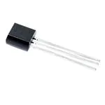
Connection Diagram
Figure 2. TO-92
Package Number LP
These devices have limited built-in ESD protection. The leads should be shorted together or the device placed in conductive foam
during storage or handling to prevent electrostatic damage to the MOS gates.
2
Submit Documentation Feedback
Copyright © 2001–2013, Texas Instruments Incorporated
Product Folder Links: LM19
�LM19
www.ti.com
SNIS122E – MAY 2001 – REVISED MARCH 2013
Absolute Maximum Ratings (1)
Supply Voltage
+6.5V to −0.2V
Output Voltage
(V+ + 0.6 V) to −0.6 V
Output Current
10 mA
Input Current at any pin (2)
5 mA
−65°C to +150°C
Storage Temperature
Maximum Junction Temperature (TJMAX)
+150°C
ESD Susceptibility (3)
2500 V
Human Body Model
Machine Model
Lead Temperature
(1)
(2)
(3)
TO-92 Package
250 V
Soldering (3 seconds dwell)
+240°C
Absolute Maximum Ratings indicate limits beyond which damage to the device may occur. Operating Ratings indicate conditions for
which the device is functional, but do not ensure specific performance limits. For ensured specifications and test conditions, see the
Electrical Characteristics. The specified specifications apply only for the test conditions listed. Some performance characteristics may
degrade when the device is not operated under the listed test conditions.
When the input voltage (VI) at any pin exceeds power supplies (VI < GND or VI > V+), the current at that pin should be limited to 5 mA.
The human body model is a 100 pF capacitor discharged through a 1.5 kΩ resistor into each pin. The machine model is a 200 pF
capacitor discharged directly into each pin.
Operating Ratings (1)
TMIN ≤ TA ≤ TMAX
Specified Temperature Range
2.4 V ≤ V+≤ 2.7 V
−30°C ≤ TA ≤ +130°C
2.7 V ≤ V+≤ 5.5 V
−55°C ≤ TA ≤ +130°C
+
Supply Voltage Range (V )
Thermal Resistance, θJA (2)
(1)
(2)
+2.4 V to +5.5 V
TO-92
150°C/W
Absolute Maximum Ratings indicate limits beyond which damage to the device may occur. Operating Ratings indicate conditions for
which the device is functional, but do not ensure specific performance limits. For ensured specifications and test conditions, see the
Electrical Characteristics. The specified specifications apply only for the test conditions listed. Some performance characteristics may
degrade when the device is not operated under the listed test conditions.
The junction to ambient thermal resistance (θJA) is specified without a heat sink in still air.
Submit Documentation Feedback
Copyright © 2001–2013, Texas Instruments Incorporated
Product Folder Links: LM19
3
�LM19
SNIS122E – MAY 2001 – REVISED MARCH 2013
www.ti.com
Electrical Characteristics
Unless otherwise noted, these specifications apply for V+ = +2.7 VDC. Boldface limits apply for TA = TJ = TMIN to TMAX ; all
other limits TA = TJ = 25°C; Unless otherwise noted.
Parameter
Conditions
Typical (1)
LM19C
Limits (2)
Temperature to Voltage Error
VO = (−3.88×10⁻⁶×T2)
+ (−1.15×10⁻²×T) + 1.8639V (3)
Units
(Limit)
TA = +25°C to +30°C
±2.5
°C (max)
TA = +130°C
±3.5
°C (max)
TA = +125°C
±3.5
°C (max)
TA = +100°C
±3.2
°C (max)
TA = +85°C
±3.1
°C (max)
TA = +80°C
±3.0
°C (max)
TA = 0°C
±2.9
°C (max)
TA = −30°C
±3.3
°C (min)
TA = −40°C
±3.5
°C (max)
TA = −55°C
±3.8
°C (max)
Output Voltage at 0°C
+1.8639
V
Variance from Curve
±1.0
°C
Non-Linearity (4)
−20°C ≤ TA ≤ +80°C
±0.4
Sensor Gain (Temperature Sensitivity
or Average Slope) to equation:
VO=−11.77 mV/°C×T+1.860V
−30°C ≤ TA ≤ +100°C
−11.77
Output Impedance
(7)
Load Regulation
Line Regulation (8)
mV/°C (min)
mV/°C (max)
0 μA ≤ IL ≤ +16 μA (5) (6)
160
Ω (max)
(5) (6)
−2.5
mV (max)
+3.7
mV/V (max)
+11
mV (max)
7
μA (max)
0 μA ≤ IL ≤ +16 μA
+2. 4 V ≤ V+ ≤ +5.0V
+5.0 V ≤ V+ ≤ +5.5 V
Quiescent Current
Change of Quiescent Current
+2. 4 V ≤ V+ ≤ +5.0V
4.5
+
+5.0V ≤ V ≤ +5.5V
4.5
9
μA (max)
+2. 4 V ≤ V+ ≤ +5.0V
4.5
10
μA (max)
+2. 4 V ≤ V+ ≤ +5.5V
+0.7
μA
−11
nA/°C
0.02
μA
Temperature Coefficient of Quiescent
Current
Shutdown Current
(1)
(2)
(3)
(4)
(5)
(6)
(7)
(8)
4
%
−11.0
−12.6
+
V ≤ +0.8 V
Typicals are at TJ = TA = 25°C and represent most likely parametric norm.
Limits are ensured to AOQL (Average Outgoing Quality Level).
Accuracy is defined as the error between the measured and calculated output voltage at the specified conditions of voltage, current, and
temperature (expressed in°C).
Non-Linearity is defined as the deviation of the calculated output-voltage-versus-temperature curve from the best-fit straight line, over
the temperature range specified.
Negative currents are flowing into the LM19. Positive currents are flowing out of the LM19. Using this convention the LM19 can at most
sink −1 μA and source +16 μA.
Load regulation or output impedance specifications apply over the supply voltage range of +2.4V to +5.5V.
Regulation is measured at constant junction temperature, using pulse testing with a low duty cycle. Changes in output due to heating
effects can be computed by multiplying the internal dissipation by the thermal resistance.
Line regulation is calculated by subtracting the output voltage at the highest supply input voltage from the output voltage at the lowest
supply input voltage.
Submit Documentation Feedback
Copyright © 2001–2013, Texas Instruments Incorporated
Product Folder Links: LM19
�LM19
www.ti.com
SNIS122E – MAY 2001 – REVISED MARCH 2013
Typical Performance Characteristics
Temperature Error vs. Temperature
Thermal Response in Still Air
5
MAX Limit
4
ERROR ( º C)
3
2
Typical
1
0
-1
-2
MIN Limit
-3
-4
-5
-100
-50
0
50
100
150
TEMPERATURE (ºC)
LM19 TRANSFER FUNCTION
The LM19's transfer function can be described in different ways with varying levels of precision. A simple linear
transfer function, with good accuracy near 25°C, is
VO= −11.69 mV/°C × T + 1.8663 V
(1)
Over the full operating temperature range of −55°C to +130°C, best accuracy can be obtained by using the
parabolic transfer function
VO = (−3.88×10⁻⁶×T2) + (−1.15×10⁻²×T) + 1.8639
(2)
solving for T:
(3)
A linear transfer function can be used over a limited temperature range by calculating a slope and offset that give
best results over that range. A linear transfer function can be calculated from the parabolic transfer function of
the LM19. The slope of the linear transfer function can be calculated using the following equation:
m = −7.76 × 10⁻⁶× T − 0.0115
where
•
T is the middle of the temperature range of interest and m is in V/°C.
(4)
For example for the temperature range of Tmin = −30 to Tmax = +100°C:
T = 35°C
and
m = −11.77 mV/°C
The offset of the linear transfer function can be calculated using the following equation:
b = (VOP(Tmax) + VOP(T) − m × (Tmax+T))/2
where
•
•
VOP(Tmax) is the calculated output voltage at Tmax using the parabolic transfer function for VO.
VOP(T) is the calculated output voltage at T using the parabolic transfer function for VO.
(5)
Using this procedure the best fit linear transfer function for many popular temperature ranges was calculated in
Table 1. As shown in Table 1 the error that is introduced by the linear transfer function increases with wider
temperature ranges.
Submit Documentation Feedback
Copyright © 2001–2013, Texas Instruments Incorporated
Product Folder Links: LM19
5
�LM19
SNIS122E – MAY 2001 – REVISED MARCH 2013
www.ti.com
Table 1. First Order Equations Optimized For Different Temperature Ranges
Temperature Range
Linear Equation
VO=
Maximum Deviation of Linear Equation from
Parabolic Equation (°C)
+130
−11.79 mV/°C × T + 1.8528 V
±1.41
+110
−11.77 mV/°C × T + 1.8577 V
±0.93
−30
+100
−11.77 mV/°C × T + 1.8605 V
±0.70
-40
+85
−11.67 mV/°C × T + 1.8583 V
±0.65
−10
+65
−11.71 mV/°C × T + 1.8641 V
±0.23
+35
+45
−11.81 mV/°C × T + 1.8701 V
±0.004
+20
+30
−11.69 mV/°C × T + 1.8663 V
±0.004
Tmin (°C)
Tmax (°C)
−55
−40
Mounting
The LM19 can be applied easily in the same way as other integrated-circuit temperature sensors. It can be glued
or cemented to a surface. The temperature that the LM19 is sensing will be within about +0.02°C of the surface
temperature to which the LM19's leads are attached.
This presumes that the ambient air temperature is almost the same as the surface temperature; if the air
temperature were much higher or lower than the surface temperature, the actual temperature measured would
be at an intermediate temperature between the surface temperature and the air temperature.
To ensure good thermal conductivity the backside of the LM19 die is directly attached to the GND pin. The
tempertures of the lands and traces to the other leads of the LM19 will also affect the temperature that is being
sensed.
Alternatively, the LM19 can be mounted inside a sealed-end metal tube, and can then be dipped into a bath or
screwed into a threaded hole in a tank. As with any IC, the LM19 and accompanying wiring and circuits must be
kept insulated and dry, to avoid leakage and corrosion. This is especially true if the circuit may operate at cold
temperatures where condensation can occur. Printed-circuit coatings and varnishes such as Humiseal and epoxy
paints or dips are often used to ensure that moisture cannot corrode the LM19 or its connections.
The thermal resistance junction to ambient (θJA) is the parameter used to calculate the rise of a device junction
temperature due to its power dissipation. For the LM19 the equation used to calculate the rise in the die
temperature is as follows:
TJ = TA + θJA [(V+ IQ) + (V+ − VO) IL]
where
•
IQ is the quiescent current and ILis the load current on the output.
(6)
Since the LM19's junction temperature is the actual temperature being measured care should be taken to
minimize the load current that the LM19 is required to drive.
Table 2 summarizes the rise in die temperature of the LM19 without any loading, and the thermal resistance for
different conditions.
Table 2. Temperature Rise of LM19 Due to Self-Heating and Thermal Resistance (θJA)
TO-92
TO-92
no heat sink
small heat fin
θJA
TJ − TA
θJA
TJ − TA
(°C/W)
(°C)
(°C/W)
(°C)
Still air
150
TBD
TBD
TBD
Moving air
TBD
TBD
TBD
TBD
6
Submit Documentation Feedback
Copyright © 2001–2013, Texas Instruments Incorporated
Product Folder Links: LM19
�LM19
www.ti.com
SNIS122E – MAY 2001 – REVISED MARCH 2013
Capacitive Loads
The LM19 handles capacitive loading well. Without any precautions, the LM19 can drive any capacitive load less
than 300 pF as shown in Figure 3. Over the specified temperature range the LM19 has a maximum output
impedance of 160 Ω. In an extremely noisy environment it may be necessary to add some filtering to minimize
noise pickup. It is recommended that 0.1 μF be added from V+ to GND to bypass the power supply voltage, as
shown in Figure 4. In a noisy environment it may even be necessary to add a capacitor from the output to ground
with a series resistor as shown in Figure 4. A 1 μF output capacitor with the 160 Ω maximum output impedance
and a 200 Ω series resistor will form a 442 Hz lowpass filter. Since the thermal time constant of the LM19 is
much slower, the overall response time of the LM19 will not be significantly affected.
Figure 3. LM19 No Decoupling Required for Capacitive Loads Less than 300 pF
Table 3. LM19 with Filter for Noisy Environment
and Capacitive Loading greater than 300 pF
R (Ω)
C (µF)
200
1
470
0.1
680
0.01
1k
0.001
Either placement of resistor as shown
above is just as effective.
Figure 4. LM19 with Filter for Noisy Environment
and Capacitive Loading greater than 300 pF
Submit Documentation Feedback
Copyright © 2001–2013, Texas Instruments Incorporated
Product Folder Links: LM19
7
�LM19
SNIS122E – MAY 2001 – REVISED MARCH 2013
www.ti.com
Applications Circuits
V+
VTEMP
R3
VT1
R4
VT2
LM4040
V+
VT
R1
4.1V
U3
0.1 PF
R2
(High = overtemp alarm)
+
U1
-
VOUT
VOUT
LM7211
VT1 =
(4.1)R2
R2 + R1||R3
VT2 =
(4.1)R2||R3
R1 + R2||R3
LM19
VTemp
U2
Figure 5. Centigrade Thermostat
Figure 6. Conserving Power Dissipation with Shutdown
Figure 7. Suggested Connection to a Sampling Analog to Digital Converter Input Stage
Most CMOS ADCs found in ASICs have a sampled data comparator input structure that is notorious for causing
grief to analog output devices such as the LM19 and many op amps. The cause of this grief is the requirement of
instantaneous charge of the input sampling capacitor in the ADC. This requirement is easily accommodated by
the addition of a capacitor. Since not all ADCs have identical input stages, the charge requirements will vary
necessitating a different value of compensating capacitor. This ADC is shown as an example only. If a digital
output temperature is required please refer to devices such as the LM74.
8
Submit Documentation Feedback
Copyright © 2001–2013, Texas Instruments Incorporated
Product Folder Links: LM19
�LM19
www.ti.com
SNIS122E – MAY 2001 – REVISED MARCH 2013
REVISION HISTORY
Changes from Revision D (March 2013) to Revision E
•
Page
Changed layout of National Data Sheet to TI format ............................................................................................................ 8
Submit Documentation Feedback
Copyright © 2001–2013, Texas Instruments Incorporated
Product Folder Links: LM19
9
�PACKAGE OPTION ADDENDUM
www.ti.com
10-Dec-2020
PACKAGING INFORMATION
Orderable Device
Status
(1)
Package Type Package Pins Package
Drawing
Qty
Eco Plan
(2)
Lead finish/
Ball material
MSL Peak Temp
Op Temp (°C)
Device Marking
(3)
(4/5)
(6)
LM19CIZ/LFT4
ACTIVE
TO-92
LP
3
2000
RoHS & Green
SN
N / A for Pkg Type
LM19CIZ/NOPB
ACTIVE
TO-92
LP
3
1800
RoHS & Green
SN
N / A for Pkg Type
LM19
CIZ
-55 to 130
LM19
CIZ
(1)
The marketing status values are defined as follows:
ACTIVE: Product device recommended for new designs.
LIFEBUY: TI has announced that the device will be discontinued, and a lifetime-buy period is in effect.
NRND: Not recommended for new designs. Device is in production to support existing customers, but TI does not recommend using this part in a new design.
PREVIEW: Device has been announced but is not in production. Samples may or may not be available.
OBSOLETE: TI has discontinued the production of the device.
(2)
RoHS: TI defines "RoHS" to mean semiconductor products that are compliant with the current EU RoHS requirements for all 10 RoHS substances, including the requirement that RoHS substance
do not exceed 0.1% by weight in homogeneous materials. Where designed to be soldered at high temperatures, "RoHS" products are suitable for use in specified lead-free processes. TI may
reference these types of products as "Pb-Free".
RoHS Exempt: TI defines "RoHS Exempt" to mean products that contain lead but are compliant with EU RoHS pursuant to a specific EU RoHS exemption.
Green: TI defines "Green" to mean the content of Chlorine (Cl) and Bromine (Br) based flame retardants meet JS709B low halogen requirements of
很抱歉,暂时无法提供与“LM19CIZ/NOPB”相匹配的价格&库存,您可以联系我们找货
免费人工找货