Sample &
Buy
Product
Folder
Support &
Community
Tools &
Software
Technical
Documents
LM21305
SNVS639G – DECEMBER 2009 – REVISED DECEMBER 2015
LM21305 3-V to 18-V, 5-A, Adjustable Frequency Synchronous Buck Converter
1 Features
2 Applications
•
•
•
•
•
1
•
•
•
•
•
•
•
•
•
•
•
•
•
•
•
High-Efficiency Synchronous DC-DC Converter:
– Integrated Low RDSon Power MOSFETs
– Wide Input Voltage Range: 3 V to 18 V
– Load Current as High as 5 A
– Switching Frequency: 300 kHz to 1.5 MHz
External Frequency Synchronization
Accurate 0.598-V Feedback Voltage Reference
Ultra-Fast Line and Load Transient Response:
– Peak Current-Mode Control
– Internal Slope Compensation
– High-Bandwidth Error Amplifier
Ultra-Low Shutdown Quiescent Current
Wide Duty-Cycle Operating Range:
– TON-MIN: 70 ns for Low VOUT
– TOFF-MIN: 50 ns for High Duty Cycle
Diode Emulation Mode at Light Loads
Integrated Bias Supply LDO Sub-Regulators
Internal Soft-Start Function:
– Monotonic Startup into Pre-Biased Loads
Precision Enable Input with Hysteresis
Open-Drain PGOOD Indicator
Internal Input Undervoltage Lockout (UVLO)
Cycle-by-Cycle Overcurrent Protection
Output Overvoltage Protection (OVP)
Thermal Shutdown Protection with Hysteresis
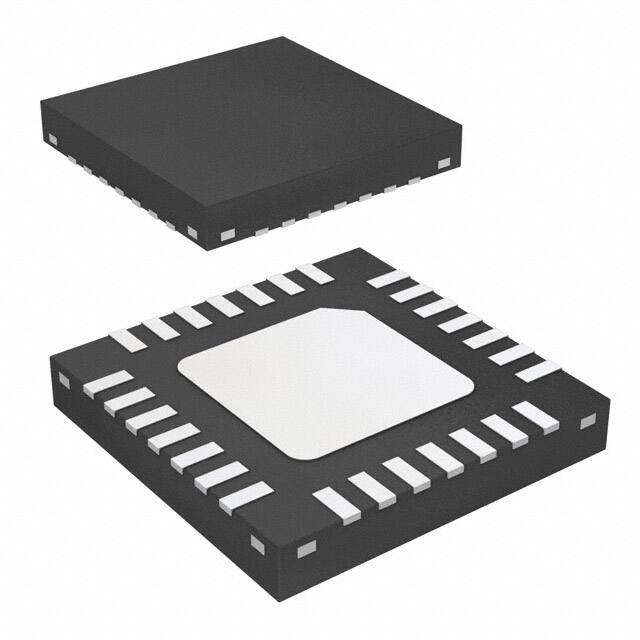
5-mm x 5-mm WQFN-28 PowerPAD™ Package
DC-DC Converters and POL Modules
DSP and FPGA Core Voltage Supplies
Telecommunications Infrastructure
Embedded Computing, Servers, and Storage
3 Description
The LM21305 is a full-featured, 5-A, synchronous
buck dc-dc converter optimized for solution size,
flexibility, and high conversion efficiency. High-power
density LM21305 designs are easily achieved by
virtue of monolithic integration of high-side and lowside power MOSFETs, high switching frequency,
peak current-mode control, and optimized thermal
design. The efficiency of the LM21305 is maximized
at light loads with diode emulation mode operation
and at heavy loads by optimal design of the MOSFET
adaptive gate drivers to minimize switch dead-times
and body-diode conduction losses.
The LM21305 accepts a wide input voltage range of
3 V to 18 V for interface to various intermediate bus
voltages, including 3.3-V, 5-V, and 12-V rails. A 1.5%
voltage reference and 70-ns, high-side MOSFET
minimum controllable on-time enable output voltages
as low as 0.598 V with excellent setpoint accuracy.
The LM21305 is available in a 5-mm × 5-mm2
WQFN-28 thermally-enhanced package with 0.5-mm
pitch.
Device Information(1)
PART NUMBER
LM21305
PACKAGE
WQFN (28)
BODY SIZE (NOM)
5.00 mm × 5.00 mm
(1) For all available packages, see the orderable addendum at
the end of the data sheet.
Typical Application Circuit
CBOOT
AVIN
LM21305
CFRQ
PGOOD
FREQ
RFRQ
2V5
VOUT = 3.3V
L
SW
EN
95
CBOOT
3.3 H
RFB1
COUT
47 F
FB
COMP
5V0
RFB2
RC
CC1
90
EFFICIENCY (%)
PVIN
SYNC
100
*VOUT tracks VIN if VIN < 3.4V
VIN = 3V...18V
CIN
10 F
Typical Efficiency at 12 V, 500 kHz
85
80
75
70
65
VOUT = 5V
VOUT = 3.3V
VOUT = 1.8V
VOUT = 1.2V
VOUT = 0.8V
60
55
AGND
PGND
50
0
1
2
3
4
LOAD CURRENT (A)
5
1
An IMPORTANT NOTICE at the end of this data sheet addresses availability, warranty, changes, use in safety-critical applications,
intellectual property matters and other important disclaimers. PRODUCTION DATA.
�LM21305
SNVS639G – DECEMBER 2009 – REVISED DECEMBER 2015
www.ti.com
Table of Contents
1
2
3
4
5
6
7
8
Features ..................................................................
Applications ...........................................................
Description .............................................................
Revision History.....................................................
Description (continued).........................................
Pin Configuration and Functions .........................
Specifications.........................................................
1
1
1
2
3
3
5
7.1
7.2
7.3
7.4
7.5
7.6
5
5
5
6
6
8
Absolute Maximum Ratings ......................................
ESD Ratings..............................................................
Recommended Operating Conditions.......................
Thermal Information ..................................................
Electrical Characteristics ..........................................
Typical Characteristics ..............................................
Detailed Description ............................................ 11
8.1 Overview ................................................................. 11
8.2 Functional Block Diagram ....................................... 11
8.3 Feature Description................................................. 12
8.4 Device Functional Modes........................................ 17
9
Application and Implementation ........................ 18
9.1 Application Information............................................ 18
9.2 Typical Application .................................................. 18
10 Power Supply Recommendations ..................... 30
11 Layout................................................................... 31
11.1 Layout Guidelines ................................................. 31
11.2 Layout Example .................................................... 33
12 Device and Documentation Support ................. 34
12.1
12.2
12.3
12.4
12.5
12.6
Device Support ....................................................
Documentation Support ........................................
Community Resources..........................................
Trademarks ...........................................................
Electrostatic Discharge Caution ............................
Glossary ................................................................
34
34
34
34
35
35
13 Mechanical, Packaging, and Orderable
Information ........................................................... 35
4 Revision History
NOTE: Page numbers for previous revisions may differ from page numbers in the current version.
Changes from Revision F (March 2013) to Revision G
Page
•
Changed Features, Applications, and Description sections and page 1 graphics ................................................................. 1
•
Added Feature Description section, ESD Ratings table, Device Functional Modes section, Application and
Implementation section, Power Supply Recommendations section, Layout section, Device and Documentation
Support section, and Mechanical, Packaging, and Orderable Information section. .............................................................. 1
•
Changed Precision Enable section....................................................................................................................................... 15
2
Submit Documentation Feedback
Copyright © 2009–2015, Texas Instruments Incorporated
Product Folder Links: LM21305
�LM21305
www.ti.com
SNVS639G – DECEMBER 2009 – REVISED DECEMBER 2015
5 Description (continued)
The LM21305 offers flexible system configuration with programmable switching frequency from 300 kHz to
1.5 MHz using one resistor or by external clock synchronization for beat-frequency-sensitive and multi-regulator
applications. On-chip bias supply low-dropout (LDO) sub-regulators eliminate the need for an external bias power
and simplify circuit board layout. The device also offers an internal soft-start to limit inrush current and provide
monotonic startup capability into unbiased and pre-biased loads, integrated boot diodes, cycle-by-cycle current
limiting, and thermal shutdown. Peak current-mode control with a high-gain error amplifier maintains stability
throughout the entire input voltage and load current ranges, enabling excellent line and load transient response.
The LM21305 features internal output overvoltage protection (OVP) and overcurrent protection (OCP) circuits for
increased system reliability. An integrated open-drain, PGOOD indicator provides output voltage monitoring,
power-rail sequencing capability, and fault indication. Other features include thermal shutdown with automatic
recovery, low PWM minimum on-time, low shutdown quiescent current, and precision enable with hysteresis for
programmable line undervoltage lockout (UVLO).
6 Pin Configuration and Functions
15
EN
PGND 9
PGND 8
10
PGND
FB 13
12
PGOOD
COMP 11
AGND
14
RSG Package
28-Pin WQFN with Exposed Thermal Pad
Top View
PGND
16 FREQ
17 AGND
SW
SW
PAD
18 AGND
19
AGND
20 AGND
SW
6
5
4
3
2
PVIN
1
PVIN
PVIN
28
24
AVIN
23
22
AVIN
21 2V5
AGND
25 5V0
26
CBOOT
27 PVIN
SW
7
Submit Documentation Feedback
Copyright © 2009–2015, Texas Instruments Incorporated
Product Folder Links: LM21305
3
�LM21305
SNVS639G – DECEMBER 2009 – REVISED DECEMBER 2015
www.ti.com
Pin Functions
PIN
NAME
NO.
Type (1)
DESCRIPTION
2V5
21
P
2.5-V output of the internal LDO regulator. Bypass to AGND with a 0.1-µF ceramic capacitor.
Loading this pin is not recommended.
5V0
25
P
5.0-V output of the internal LDO regulator. Bypass to PGND with a 1-µF ceramic capacitor.
Loading this pin is not recommended.
AGND
14, 17–20, 24
G
Analog ground for the internal bias circuitry and signal return connection for analog functions,
including COMP network, frequency adjust resistor, and 2V5 decoupling capacitor.
AVIN
22, 23
P
Analog power input. AVIN powers the internal 2.5-V and 5.0-V LDOs that provide bias
current and internal driver power, respectively. AVIN can be connected to PVIN through a
low-pass RC filter or can be supplied by a separate rail.
CBOOT
26
P
High-side bootstrap connection to drive the high-side MOSFET. Connect a 100-nF bootstrap
capacitor between the CBOOT and SW pins.
COMP
11
A
Compensation node. This pin is an output voltage control loop error amplifier output.
Connect an external compensation network to ensure stability.
EN
15
I
Precision enable pin. Use an external divider to set the device turn-on threshold. If not used,
connect the EN pin to AVIN.
FB
13
A
Voltage feedback pin. Connect this pin to the output voltage directly or through a resistor
divider to set the output voltage range.
FREQ
16
A
Frequency adjust pin. Connect a resistor from FREQ to AGND to set the internal oscillator
frequency. Connect FREQ to an external clock source via a coupling capacitor to
synchronize to the external clock frequency.
PVIN
1, 2, 27, 28
P
Input voltage to the power MOSFETs inside the device.
3-6
P
Switch node output of the power MOSFETs. Voltage swings from PVIN to GND on this pin.
SW also delivers current to the external inductor.
7–10
G
Power ground connection for the internal power switches.
12
OD
Open-drain output with 16 μs of built-in deglitch time. If high, this status pin indicates that the
output voltage is regulated within tolerance. Connect a 10-kΩ to 100-kΩ resistor to a pullup
voltage source, for example the 5V0 rail or auxiliary system voltage rail.
PAD
—
Exposed pad at the back of the device. Connect PAD to PGND, but PAD cannot be used as
the primary ground connection. Use multiple vias under PAD to connect to the system
ground plane for optimal thermal performance.
SW
PGND
PGOOD
PAD
(1)
4
P: Power, A: Analog, I: Digital Input, OD: Open Drain, G: Ground.
Submit Documentation Feedback
Copyright © 2009–2015, Texas Instruments Incorporated
Product Folder Links: LM21305
�LM21305
www.ti.com
SNVS639G – DECEMBER 2009 – REVISED DECEMBER 2015
7 Specifications
7.1 Absolute Maximum Ratings
see
(1) (2)
MIN
MAX
UNIT
PVIN, AVIN, SW, EN, PGOOD to AGND
−0.3
20
V
CBOOT to AGND
−0.3
25
V
CBOOT to SW
−0.3
5.5
V
5V0, FB, COMP, FREQ to AGND
−0.3
6
V
2V5 to AGND
−0.3
3
V
AGND to PGND
−0.3
0.3
V
Maximum continuous power dissipation, PD-MAX (3)
Internally limited
Junction temperature, TJ-MAX
Storage temperature, Tstg
(1)
(2)
(3)
–65
150
°C
150
°C
Stresses beyond those listed under absolute maximum ratings may cause permanent damage to the device. These are stress ratings
only, and functional operation of the device at these or any other conditions beyond those indicated under recommended operating
conditions is not implied. Exposure to absolute-maximum-rated conditions for extended periods may affect device reliability.
If Military or Aerospace specified devices are required, please contact the Texas Instruments Sales Office/Distributors for availability and
specifications.
The amount of absolute maximum power dissipation allowed in the device depends on the ambient temperature and can be calculated
using the formula P = (TJ – TA) / θJA, where TJ is the junction temperature, TA is the ambient temperature, and θJA is the junction-toambient thermal resistance. Junction-to-ambient thermal resistance is highly application and board-layout dependent. In applications
where high power dissipation exists, special care must be paid to thermal dissipation issues in PCB design. Internal thermal shutdown
circuitry protects the device from permanent damage.
7.2 ESD Ratings
VALUE
V(ESD)
(1)
(2)
(3)
Electrostatic discharge
Human body model (HBM), per ANSI/ESDA/JEDEC JS-001
(1) (2)
UNIT
±2000
Charged device model (CDM), per JEDEC specification JESD22-C101 (3)
V
±500
JEDEC document JEP155 states that 500-V HBM allows safe manufacturing with a standard ESD control process. Manufacturing with
less than 500-V HBM is possible with the necessary precautions. Pins listed as ±2000 V may actually have higher performance.
The human body model is a 100-pF capacitor discharged through a 1.5-kΩ resistor into each pin (MIL-STD-883 3015.7).
JEDEC document JEP157 states that 250-V CDM allows safe manufacturing with a standard ESD control process. Manufacturing with
less than 250-V CDM is possible with the necessary precautions. Pins listed as ±500 V may actually have higher performance.
7.3 Recommended Operating Conditions
PVIN to PGND, AGND
AVIN to PGND, AGND
MIN
MAX
3
18
UNIT
V
3
18
V
Junction temperature
−40
125
°C
Ambient temperature (1)
–40
85
°C
(1)
In applications where high power dissipation or poor package thermal resistance is present, the maximum ambient temperature may
have to be derated. Maximum ambient temperature (TA-MAX) is dependent on the maximum operating junction temperature (TJ-MAX-OP =
125°C), the maximum power dissipation of the device in the application (PD-MAX), and the junction-to ambient thermal resistance of the
part or package in the application (θJA), as given by the following equation: TA-MAX = TJ-MAX-OP – (θJA × PD-MAX).
Submit Documentation Feedback
Copyright © 2009–2015, Texas Instruments Incorporated
Product Folder Links: LM21305
5
�LM21305
SNVS639G – DECEMBER 2009 – REVISED DECEMBER 2015
www.ti.com
7.4 Thermal Information
LM21305
THERMAL METRIC (1)
RSG (WQFN)
UNIT
28 PINS
RθJA
Junction-to-ambient thermal resistance
36.9
°C/W
RθJC(top)
RθJB
Junction-to-case (top) thermal resistance
22
°C/W
Junction-to-board thermal resistance
9.9
°C/W
ψJT
Junction-to-top characterization parameter
0.2
°C/W
ψJB
Junction-to-board characterization parameter
9.8
°C/W
RθJC(bot)
Junction-to-case (bottom) thermal resistance
2.1
°C/W
(1)
For more information about traditional and new thermal metrics, see the Semiconductor and IC Package Thermal Metrics application
report, SPRA953.
7.5 Electrical Characteristics
All typical limits apply for TJ = 25°C, and all maximum and minimum limits apply over the full operating temperature range (TJ
= –40°C to +125°C). Unless otherwise specified, VIN = VPVIN = VAVIN = 12 V, VOUT = 3.3 V, IOUT = 0 A. (1) (2) (2)
PARAMETER
TEST CONDITIONS
MIN
TYP
MAX
UNIT
0.588
0.598
0.608
V
GENERAL
VFB-default
Feedback pin factory-default voltage
ΔVOUT/ΔIOUT
Load regulation
IOUT = 0.1 A to 5 A
0.02
%/A
ΔVOUT/ΔVIN
Line regulation
VPVIN = 3 V to 18 V
0.01
%/V
RDSonHS
High-side switch on-resistance
IDS = 5 A
44
mΩ
RDSonLS
Low-side switch on-resistance
IDS = 5 A
ICL-HS
High-side switch current limit
High-side MOSFET
5.9
7
7.87
A
ICL-LS
Low-side switch current limit
Low-side MOSFET (3)
5.9
8
10.2
A
INEG-CL-LS
Low-side switch negative current limit
Low-side MOSFET
–7
–4.1
–1.64
A
ISD
Quiescent current, disabled
22
mΩ
VAVIN = V
PVIN
=5V
0.1
2
VAVIN = V
PVIN
= 18 V
1
4.1
9
9.7
IQ
Quiescent current, enabled, not
switching
VAVIN = V PVIN = 18 V
IFB
Feedback pin input bias current
VFB = 0.598 V
GM
Error amplifier transconductance
AVOL
Error amplifier voltage gain
VIH-OVP
OVP tripping threshold
Rising threshold, percentage of VOUT
VHYST-OVP
OVP hysteresis window
Percentage of VOUT
VUVLO-HI-AVIN
AVIN UVLO rising threshold
2.84
2.93
2.987
VUVLO-LO-AVIN
AVIN UVLO falling threshold
2.66
2.73
2.83
VUVLO-HYS-AVIN
AVIN UVLO hysteresis window
V5V0
Internal LDO1 output voltage
COUT-CAP-5V0
Recommended capacitance connected
Ceramic capacitor
to 5V0 pin
(1)
(2)
(3)
6
mA
1
nA
2400
µs
65
Measured at 5V0 pin, 1-kΩ load
µA
103.5% 109.5%
dB
115%
–4.3%
V
V
195
mV
4.88
V
1
µF
All limits are specified by design, test or statistical analysis. All electrical characteristics having room-temperature limits are tested during
production with TJ = 25°C. All hot and cold limits are specified by correlating the electrical characteristics to process and temperature
variations and applying statistical process control.
Capacitors: low ESR surface-mount ceramic capacitors (MLCCs) are used in setting electrical characteristics.
The low-side switch current limit is ensured to be higher than the high-side current limit.
Submit Documentation Feedback
Copyright © 2009–2015, Texas Instruments Incorporated
Product Folder Links: LM21305
�LM21305
www.ti.com
SNVS639G – DECEMBER 2009 – REVISED DECEMBER 2015
Electrical Characteristics (continued)
All typical limits apply for TJ = 25°C, and all maximum and minimum limits apply over the full operating temperature range (TJ
= –40°C to +125°C). Unless otherwise specified, VIN = VPVIN = VAVIN = 12 V, VOUT = 3.3 V, IOUT = 0 A.(1)(2)(2)
PARAMETER
TEST CONDITIONS
MIN
TYP
MAX
UNIT
GENERAL (continued)
ISHORT-5V0
Short-circuit current of 5V0 pin
V2V5
Internal LDO2 output voltage
31
COUT-CAP-2V5
Recommended capacitance connected Ceramic capacitor
to 2V5 pin
ISHORT-2V5
Short-circuit current of 2V5 pin
VFCBOOT-D
CBOOT diode forward voltage
Measured from 5V0 to CBOOT at 10 mA
0.76
V
ICBOOT
CBOOT leakage current
VCBOOT = 5.5 V, not switching
0.65
µA
TSTARTUP-DELAY
Startup time from EN high to the
beginning of internal soft-start
160
µs
SS
Internal soft-start
10% to 90% VFB
1.41
2.7
4.15
ms
FOSC-NOM
Oscillator frequency, nominal
measured at SW pin
RFRQ = 61.9 kΩ, 0.025%
695
750
795
kHz
FOSC-MAX
Maximum oscillator frequency
measured at SW pin
RFRQ = 28.4 kΩ
1500
kHz
FOSC-MIN
Minimum oscillator frequency
measured at SW pin
RFRQ = 167.5 kΩ
300
kHz
TOFF-MIN
Minimum off-time measured at SW pin
FSW = 1.5 MHz, VIN = 3.3 V, VFB = 1 V,
voltage divider ratio = 3.3
50
ns
TON-MIN
Minimum on-time measured at SW pin FSW = 1.5 MHz, voltage divider ratio = 1
70
ns
Measured at 2V5 pin, 1-kΩ load
mA
2.47
V
100
nF
47
mA
OSCILLATOR
LOGIC
VIH-EN
EN pin rising threshold
1.1
1.2
1.3
V
VHYST-EN
EN pin hysteresis window
130
200
302
mV
IEN-IN
EN pin input current
VEN = 12 V
18
23
µA
VIH-UV-PGOOD
PGOOD UV rising threshold
Percentage of VOUT
93%
97.5%
VHYST-UV-PGOOD
PGOOD UV hysteresis threshold
Percentage of VOUT
IOL-
PGOOD sink current
VOL = 0.2 V
PGOOD leakage current
VOH = 18 V
PGOOD
IOH- PGOOD
87.5%
–4.2%
3
mA
460
nA
THERMAL SHUTDOWN
TSD
Thermal shutdown (4)
TSD-HYS
Thermal shutdown hysteresis (4)
(4)
160
°C
10
°C
Specified by design.
Submit Documentation Feedback
Copyright © 2009–2015, Texas Instruments Incorporated
Product Folder Links: LM21305
7
�LM21305
SNVS639G – DECEMBER 2009 – REVISED DECEMBER 2015
www.ti.com
7.6 Typical Characteristics
100
100
95
95
90
90
EFFICIENCY (%)
EFFICIENCY (%)
VIN = 12 V, VOUT = 3.3 V, FSW = 500 kHz, TA = 25°C, L = 3.3 µH, and COUT = 100 µF (ceramic), (unless otherwise specified)
85
80
75
70
65
VOUT = 3.3V
VOUT = 1.8V
VOUT = 1.2V
VOUT = 0.8V
60
55
50
0
1
2
3
4
LOAD CURRENT (A)
70
65
0
95
95
90
90
85
80
75
70
65
VOUT = 3.3V
VOUT = 1.8V
VOUT = 1.2V
VOUT = 0.8V
50
0
1
2
3
4
LOAD CURRENT (A)
80
75
70
65
50
0
5
95
90
90
EFFICIENCY (%)
100
85
80
75
70
65
VOUT = 3.3V
VOUT = 1.8V
VOUT = 1.2V
VOUT = 0.8V
1
2
3
4
LOAD CURRENT (A)
5
Figure 4. Efficiency with PVIN = AVIN = 12 V
95
0
1
FSW = 500 kHz
100
50
VOUT = 5V
VOUT = 3.3V
VOUT = 1.8V
VOUT = 1.2V
VOUT = 0.8V
55
Figure 3. Efficiency with PVIN = AVIN = 5 V
55
5
85
60
FSW = 500 kHz
60
2
3
4
LOAD CURRENT (A)
Figure 2. Efficiency with PVIN = AVIN = 12 V
100
55
1
FSW = 300 kHz
100
60
VOUT = 5V
VOUT = 3.3V
VOUT = 1.8V
VOUT = 1.2V
VOUT = 0.8V
50
5
EFFICIENCY (%)
EFFICIENCY (%)
75
55
Figure 1. Efficiency with PVIN = AVIN = 5 V
EFFICIENCY (%)
80
60
FSW = 300 kHz
2
3
4
LOAD CURRENT (A)
85
80
75
70
65
VOUT = 5V
VOUT = 3.3V
VOUT = 1.8V
VOUT = 1.2V
VOUT = 0.8V
60
55
50
0
5
1
2
3
4
LOAD CURRENT (A)
5
FSW = 1 MHz
FSW = 1 MHz
Figure 5. Efficiency with PVIN = AVIN = 5 V
8
85
Figure 6. Efficiency with PVIN = AVIN = 12 V
Submit Documentation Feedback
Copyright © 2009–2015, Texas Instruments Incorporated
Product Folder Links: LM21305
�LM21305
www.ti.com
SNVS639G – DECEMBER 2009 – REVISED DECEMBER 2015
Typical Characteristics (continued)
VIN = 12 V, VOUT = 3.3 V, FSW = 500 kHz, TA = 25°C, L = 3.3 µH, and COUT = 100 µF (ceramic), (unless otherwise specified)
0.10
LINE REGULATION (%)
LOAD REGULATION (%)
0.10
0.05
0.00
-0.05
-0.10
1
2
3
4
LOAD CURRENT (A)
-0.05
5
3
Figure 7. Load Regulation (% VOUT)
QUIESCENT CURRENT (mA)
0.0
-0.5
-1.0
9
8
7
6
-40°C
25°C
85°C
5
-20
0
20 40 60
TEMPERATURE (°C)
80
100
Figure 9. VOUT Regulation (%) vs Temperature
3
6
9
12
15
INPUT VOLTAGE (V)
18
Figure 10. Input Quiescent Current, Not Switching
70
1800
High-Side RDSon(m )
1600
FREQUENCY (kHz)
60
18
10
0.5
-40
6
9
12
15
INPUT VOLTAGE, PVIN (V)
Figure 8. Line Regulation (% VOUT)
1.0
VOUTREGULATION (%)
0.00
-0.10
0
50
RDSON(m )
0.05
40
30
20
1400
1200
1000
800
600
400
10
200
Low-Side RDSon(m )
0
0
-40
-20
0
20
40
60
TEMPERATURE (°C)
80
100
Figure 11. High-Side and Low-Side MOSFET RDS(on)
vs Temperature
-40°C
25°C
125°C
0 20 40 60 80 100 120 140 160 180
RFRQ(k )
Figure 12. Switching Frequency vs RFRQ
Submit Documentation Feedback
Copyright © 2009–2015, Texas Instruments Incorporated
Product Folder Links: LM21305
9
�LM21305
SNVS639G – DECEMBER 2009 – REVISED DECEMBER 2015
www.ti.com
Typical Characteristics (continued)
VIN = 12 V, VOUT = 3.3 V, FSW = 500 kHz, TA = 25°C, L = 3.3 µH, and COUT = 100 µF (ceramic), (unless otherwise specified)
IOUT 1A/DIV
EN 1V/DIV
VOUT 1V/DIV
PGOOD 1V/DIV
PGOOD 1V/DIV
EN 1V/DIV
VOUT
1V/DIV
IOUT 1A/DIV
2 ms/DIV
2 ms/DIV
Figure 13. Soft-Start, No Load
Figure 14. Soft-Start with Resistive Load
EN 1V/DIV
VOUT 1V/DIV
PGOOD 1V/DIV
IOUT 1A/DIV
2 ms/DIV
10
Figure 15. Soft-Start with 2-V Pre-Bias Voltage, No Load
Figure 16. Switching Waveform with No Load Connected
(DCM Operation)
Figure 17. Switching Waveform with 5-A Load
Figure 18. Load Transient Response, 0.1 A to 5 A
Submit Documentation Feedback
Copyright © 2009–2015, Texas Instruments Incorporated
Product Folder Links: LM21305
�LM21305
www.ti.com
SNVS639G – DECEMBER 2009 – REVISED DECEMBER 2015
8 Detailed Description
8.1 Overview
The LM21305 employs a current-mode control loop with slope compensation to accurately regulate the output
voltage over substantial load, line, and temperature ranges. The switching frequency is programmable between
300 kHz and 1.5 MHz through a resistor or an external synchronization signal. The LM21305 is available in a
thermally-enhanced WQFN-28 packages with 0.5-mm lead pitch. The device offers high levels of integration by
including power MOSFETs, low-dropout (LDO) bias supply regulators, and comprehensive fault protection
features to enable highly flexible, reliable, energy-efficient, and high density regulator solutions. Multiple fault
conditions are accommodated, including overvoltage, undervoltage, overcurrent, and overtemperature.
The 0.598-V reference is compared to the feedback signal at the error amplifier (EA). The PWM modulator block
compares the on-time current sense information with the summation of the EA output (control voltage) and slope
compensation signal. The PWM modulator outputs on and off signals to the high-side and low-side MOSFET
drivers. Adaptive dead-time control is applied to the PWM output such that MOSFET shoot-through current is
avoided. The drivers then amplify the PWM signals to control the integrated high-side and low-side MOSFETs.
8.2 Functional Block Diagram
C7
R1
C6
C5
AVIN
2V5
CBOOT
5V0
VIN
LDO1
5V
LDO2
2.5V
PVIN
C1
OTP
ISENSE
UVLO
HS
FET
OCP
C2
SS
Nonoverlap
EN
+
L1
VOUT
EA
REF
PWM
PWM Control Logic
1.2V
PGOOD
Slope
Comp
Input
UVLO
Output
UV, OV
AGND
OVP
SW
Z cross
LS FET OCP
Rev OCP
OTP
C3
Nonoverlap
FB
OSC/
Sync
COMP
FREQ
SYNC
PGND
R1
C5
R4
C4
Submit Documentation Feedback
Copyright © 2009–2015, Texas Instruments Incorporated
Product Folder Links: LM21305
11
�LM21305
SNVS639G – DECEMBER 2009 – REVISED DECEMBER 2015
www.ti.com
8.3 Feature Description
8.3.1 Synchronous DC-DC Switching Converter
The LM21305 employs a buck type (step-down) dc-dc converter architecture. The device uses many advanced
features to achieve excellent voltage regulation and efficiency. This easy-to-use regulator has two integrated
power MOSFET switches and is capable of supplying up to 5 A of continuous output current. The regulator uses
peak current-mode control with slope compensation scaled with switching frequency to optimize stability and
transient response over the entire output voltage and switching frequency ranges. Peak current-mode control
also provides inherent line feed-forward, cycle-by-cycle current limiting, and easy loop compensation. The
switching frequency is adjusted between 300 kHz and 1.5 MHz. The device can operate with a small external LC
filter and still provides very low output voltage ripple. The precision internal voltage reference allows the output to
be set as low as 0.598 V. Using an external compensation circuit, the regulator crossover frequency can be
selected based on the switching frequency to provide fast line and load transient response.
The switching regulator is specifically designed for highly-efficient operation throughout the load range.
Synchronous rectification yields high efficiency for low output voltage and heavy load current situations, whereas
discontinuous conduction mode (DCM) and diode emulation mode (DEM) enable high-efficiency conversion at
lighter load current conditions. Fault protection features include: high-side and low-side MOSFET current limiting,
negative current limiting on the low-side MOSFET, overvoltage protection, and thermal shutdown. The device is
available in a WQFN-28 package featuring an exposed pad to aid thermal dissipation. Use the LM21305 in
numerous applications to efficiently step-down from a wide range of input rails: 3 V to 18 V.
8.3.2 Peak Current-Mode Control
In most applications, the peak current-mode control architecture used in the LM21305 requires only two external
components to achieve a stable design. External compensation allows the user to set the crossover frequency
and phase margin, thus optimizing the transient performance of the device. For duty cycles above 50%, all peak
current-mode controlled buck converters require the addition of an additional ramp to avoid sub-harmonic
oscillation. This linear ramp is commonly referred to as slope compensation. The amount of slope compensation
in the LM21305 automatically changes depending on the switching frequency: the higher the switching
frequency, the larger the slope compensation. This adaptive amplitude slope compensation feature facilitates use
of smaller inductors in high-switching frequency applications where higher power density is critical.
8.3.3 Switching Frequency Setting and Synchronization
The LM21305 switching regulator operates over a frequency ranging from 300 kHz to 1.5 MHz. The switching
frequency is set or controlled in two ways. One is by selecting the external resistor connected to the FREQ pin to
set the internal free-running oscillator frequency that determines the switching frequency. Connect an external
100-pF capacitor, CFRQ, from FREQ to AGND as a noise filter, as shown in Figure 19.
LM21305
CFRQ
FREQ
RFRQ
Figure 19. Switching Frequency Set by External Resistor
The other way is to synchronize the switching frequency to an external clock in the range of 300 kHz to 1.5 MHz.
Apply the external clock through a 100-pF coupling capacitor, CFRQ, as shown in Figure 20.
LM21305
CFRQ
FREQ
External
Clock
RFRQ
Figure 20. Switching Frequency Synchronized to the External Clock
12
Submit Documentation Feedback
Copyright © 2009–2015, Texas Instruments Incorporated
Product Folder Links: LM21305
�LM21305
www.ti.com
SNVS639G – DECEMBER 2009 – REVISED DECEMBER 2015
Feature Description (continued)
The recommendations for the external clock include peak-to-peak voltage above 1.5 V, duty cycle between 20%
and 80%, and an edge rate faster than 100 ns. Circuits that use an external clock must still use a resistor
connected from FREQ to AGND. The external clock frequency must be within –10% to +50% of the free-running
frequency set by RFRQ. This arrangement allows the regulator to continue operating at approximately the same
switching frequency if the external clock fails and the coupling capacitor on the clock side is grounded or pulled
to logic high.
If the external clock fails low, timeout circuits prevent the high-side MOSFET from staying off for longer than 1.5
times the switching period, TSW = 1 / FSW. At the end of this timeout period, the regulator begins to switch at the
frequency set by RFRQ.
If the external clock fails high, timeout circuits again prevent the high-side MOSFET from staying off longer than
1.5 times the switching period. After this timeout period, the internal oscillator takes over and switches at a fixed
1 MHz until the voltage on the FREQ pin has decayed to approximately 0.6 V. This decay follows the time
constant of CFRQ and RFRQ and, when complete, the regulator switches at the frequency set by RFRQ.
8.3.4 Light-Load Operation
The LM21305 offers increased efficiency at light loads by allowing discontinuous conduction mode (DCM). When
the load current is less than half of the inductor ripple current the device enters DCM, thus preventing negative
inductor current. The output current at the critical conduction boundary is calculated according to Equation 1:
IBOUNDARY
'IL
2
VOUT ˜ 1 D
2 ˜ L ˜ FSW
where
•
D is the duty cycle of the high-side MOSFET, equal to the high-side MOSFET on-time divided by the switching
period
(1)
For more details, see the Calculating the Duty Cycle subsection in the Detailed Design Procedure section.
Several diagrams are provided in Figure 21 that illustrate continuous conduction mode (CCM), discontinuous
conduction mode (DCM), and the boundary condition. In DCM, whenever the inductor current reaches zero the
SW node becomes high impedance. Ringing occurs on this pin as a result of the LC tank circuit formed by the
inductor and the effective parasitic capacitance at the switch node. At very light loads, usually below 100 mA,
several pulses are skipped in between switching cycles, effectively reducing the switching frequency and further
improving light-load efficiency.
Submit Documentation Feedback
Copyright © 2009–2015, Texas Instruments Incorporated
Product Folder Links: LM21305
13
�LM21305
SNVS639G – DECEMBER 2009 – REVISED DECEMBER 2015
www.ti.com
Switchnode Voltage
Feature Description (continued)
Continuous Conduction Mode (CCM)
VIN
Inductor Current
Time (s)
Continuous Conduction Mode (CCM)
IAVERAGE
Inductor Current
Time (s)
DCM - CCM Boundary
IAVERAGE
Switchnode Voltage
Time (s)
Discontinuous Conduction Mode (DCM)
VIN
Inductor Current
Time (s)
Discontinuous Conduction Mode (DCM)
IPeak
Time (s)
Figure 21. CCM and DCM Operation
14
Submit Documentation Feedback
Copyright © 2009–2015, Texas Instruments Incorporated
Product Folder Links: LM21305
�LM21305
www.ti.com
SNVS639G – DECEMBER 2009 – REVISED DECEMBER 2015
Feature Description (continued)
8.3.5 Precision Enable
The enable (EN) pin allows the output of the device to be enabled or disabled with an external control signal.
This pin is a precision analog input that enables the device when the voltage exceeds 1.2 V (typical). The EN pin
has 200 mV (typical) of hysteresis and disables the output when the enable voltage falls below 1.0 V (typical). If
the EN pin is not used, pull this pin up to AVIN via a 10-kΩ to 100-kΩ resistor. Given that EN has a precise turnon threshold, use an external resistor divider network from an external voltage to configure the device to turn on
at a precise voltage. The precision enable circuits remains active even when the device is disabled. From
Figure 22, calculate the turn-on voltage with a divider using Equation 2:
VEN
EXT
§ REN1 ·
1.2 V ˜ ¨ 1
¸
© REN2 ¹
(2)
VEN-EXT
LM21305
REN1
EN
REN2
Figure 22. Use an External Resistor Divider to Set the EN Threshold
8.3.6 Device Enable, Soft-Start, and Pre-Bias Startup Capability
The LM21305 can be turned off by removing AVIN or by pulling the EN pin low. To enable the device, the EN pin
must be high with the presence of AVIN and PVIN. When enabled, the device engages the internal soft-start
circuit. The soft-start feature allows the regulator output to gradually reach the steady-state operating point, thus
reducing stresses on the input supply and controlling startup current. Soft-start begins at the rising edge of EN
with AVIN above the UVLO level. PVIN must be high when soft-start begins. The LM21305 allows AVIN to be
higher than PVIN, or PVIN higher than AVIN, provided that both voltages are within their operating ranges.
Soft-start of the LM21305 is controlled internally, and 2.7 ms is typically required to finish the soft-start sequence.
PGOOD transitions high after soft-start is complete.
The LM21305 is in a pre-biased state when the device initiates startup with an output voltage greater than zero.
This condition often occurs in multi-rail applications, such as when powering an field-programmable gate array
(FPGA), application-specific integrated circuit (ASIC), or digital signal processor (DSP) loads. In these
applications, the output can be pre-biased through parasitic conduction paths from one supply rail to another.
Even though the LM21305 is a synchronous converter, the device does not pull the output low when a pre-bias
condition exists. During startup, the LM21305 is in diode emulation mode with the low-side MOSFET turned off
when zero crossing of the inductor current is detected.
Submit Documentation Feedback
Copyright © 2009–2015, Texas Instruments Incorporated
Product Folder Links: LM21305
15
�LM21305
SNVS639G – DECEMBER 2009 – REVISED DECEMBER 2015
www.ti.com
Feature Description (continued)
8.3.7 Peak Current Protection and Negative Current Limiting
The LM21305 switching regulator detects the peak inductor current and limits it to 7 A, typical. To determine the
average current from the peak current, the inductor size, input and output voltage, and switching frequency must
be known. The average current limit is found from Equation 3:
IAVE
LIMIT
IPEAK
LIMIT
'IL
2
(3)
When the peak inductor current sensed in the high-side MOSFET reaches the current limit threshold, an
overcurrent event is triggered, the high-side MOSFET turns off and the low-side MOSFET turns on, allowing the
inductor current to ramp down until the next switching cycle. When the high-side overcurrent condition persists,
the output voltage is decreased by the reduced high-side MOSFET on-time.
In cases such as output short-circuit or when high-side MOSFET minimum on-time conditions are reached, the
high-side MOSFET current limiting may not be sufficient to limit the inductor current. The LM21305 features an
additional low-side MOSFET current limit to prevent the inductor current from running away. The low-side
MOSFET current limit, 8 A typical, is set higher than the high-side current limit. When the low-side MOSFET
current is higher than the limit level, PWM pulses are skipped until a low-side overcurrent is not detected during
the entire low-side MOSFET conduction time. Normal PWM switching subsequently occurs when the condition is
removed. High-side and low-side MOSFET current protections result in a current limit that does not aggressively
foldback for brief overcurrent events, and at the same time provides frequency and voltage foldback protection
during hard short-circuit conditions. The low-side MOSFET also has a negative current limit, –4.1 A typical, for
secondary protection that can engage during response to overvoltage events. If the negative current limit is
triggered, the low-side MOSFET is turned off. The negative current is forced to go through the high-side
MOSFET body diode and quickly reduces.
8.3.8 PGOOD Indicator
To implement an open-drain, power-good function for sequencing and fault detection, use the PGOOD pin of the
LM21305. The PGOOD open-drain MOSFET is pulled low during output undervoltage and overvoltage, UVLO,
and thermal shutdown. The PGOOD function has a 16-µs glitch filter to prevent false-flag operation for short
excursions in the output voltage, such as during line and load transients. When the FB voltage is typically within
–7% to 9.5% of the reference voltage, PGOOD is high. The thresholds track with the output voltage because the
PGOOD comparator and the regulation loop share the same reference. Pull PGOOD high with an external
resistor (10 kΩ to 100 kΩ is recommended) to an external logic supply. PGOOD can also be pulled-up to either
the 5V0 rail or to the output voltage through an appropriate resistor, as desired. Tie PGOOD to AGND if the
function is not required.
8.3.9 Internal Bias Regulators
The LM21305 contains two internal low dropout (LDO) regulators to produce internal driving and bias voltage
rails from AVIN. One LDO produces 5 V to power the internal MOSFET drivers, the other LDO produces 2.5 V to
power the internal bias circuitry. Bypass both the 5V0 or 2V5 LDOs to the analog ground (AGND) with an
external ceramic capacitor (1 μF and 0.1 μF are recommended, respectively). Good bypassing is necessary to
supply the high transient currents required by the power MOSFET gate drivers. Applications with high input
voltage and high switching frequency increase die temperature because of the higher power dissipation within
the LDOs. Connecting a load to the 5V0 or 2V5 pins is not recommended because doing so degrades their
driving capability to internal circuitry, further pushing the LDOs into their RMS current ratings and increasing
power dissipation and die temperature.
The LM21305 allows AVIN to be as low as 3 V, which makes the voltage at the 5V0 LDO lower than 5 V. Low
supply voltage at the MOSFET drivers increases on-state resistance of the high-side and low-side power
MOSFETs and reduces efficiency of the regulator. When AVIN is between 3 V and 5.5 V, the best practice is to
short the 5V0 pin to AVIN to avoid the voltage drop on the internal LDO. However, the device can be damaged if
the 5V0 pin is pulled to a voltage higher than 5.5 V. For efficiency considerations, use AVIN = 5 V if possible.
When AVIN is above 5 V, reduced efficiency can be observed at light load because of the power loss of the
LDOs. When AVIN is close to 3 V, increased MOSFET on-state resistance can reduce efficiency at high load
currents.
16
Submit Documentation Feedback
Copyright © 2009–2015, Texas Instruments Incorporated
Product Folder Links: LM21305
�LM21305
www.ti.com
SNVS639G – DECEMBER 2009 – REVISED DECEMBER 2015
Feature Description (continued)
8.3.10 Minimum On-Time Considerations
Minimum on-time, TON-MIN, is the smallest duration of time that the high-side MOSFET conducts, typically 70 ns in
the LM21305. In CCM operation, the minimum on-time limit corresponds to a minimum duty cycle as shown in
Equation 4:
DMIN
FSW ˜ TON
(4)
MIN
The minimum on-time becomes relevant when operating simultaneously at high input voltage and high switching
frequency. As Equation 4 shows, reducing the operating frequency alleviates the minimum on-time constraint.
For a given switching frequency and output voltage, the maximum PVIN is approximated by Equation 5:
VPVIN(max)
VOUT
1
˜
FSW TON MIN
(5)
Similarly, if the input voltage is fixed, the maximum switching frequency without reaching the minimum on-time
constraint is found by Equation 6:
FSW (max)
VOUT
˜
1
VPVIN(max) TON
(6)
MIN
In rare cases where steady-state operation at minimum duty cycle is unavoidable, the regulator automatically
skips cycles to keep VOUT regulated, similar to light-load DCM operation.
8.4 Device Functional Modes
8.4.1 Overvoltage and Undervoltage Handling
The LM21305 has built-in undervoltage protection (UVP) and overvoltage protection (OVP) using FB voltage
comparators to control the power MOSFETs. The rising OVP threshold is typically set at 109.5% of the nominal
voltage setpoint. Whenever excursions occur in the output voltage above the OVP threshold, the device
terminates the present on-pulse, turns on the low-side MOSFET, and pulls PGOOD low. The low-side MOSFET
remains on until either the FB voltage falls back into regulation or the inductor current zero-cross is detected. If
the output reaches the falling UVP threshold, typically 88.8% of the nominal setpoint, the device continues
switching and PGOOD is asserted and pulls low. As detailed in the PGOOD Indicator section, PGOOD has 16 μs
of built-in deglitch time to both the rising and falling edges to avoid false tripping during transient glitches. OVP is
disabled during soft-start to prevent false triggering.
8.4.2 Undervoltage Lockout (UVLO)
The LM21305 has a built-in undervoltage lockout (UVLO) protection circuit that prevents the device from
switching until the AVIN voltage reaches 2.93 V (typical). The UVLO threshold has typically 195 mV of hysteresis
that keeps the device from responding to power-on glitches during startup.
8.4.3 Thermal Protection
Internal thermal shutdown circuitry is provided to protect the LM21305 in the event that the maximum junction
temperature is exceeded. When activated, typically at 160°C, the LM21305 turns off the power MOSFETs and
resets soft-start. After the junction temperature cools to approximately 150°C, the LM21305 starts up using the
normal startup routine.
Submit Documentation Feedback
Copyright © 2009–2015, Texas Instruments Incorporated
Product Folder Links: LM21305
17
�LM21305
SNVS639G – DECEMBER 2009 – REVISED DECEMBER 2015
www.ti.com
9 Application and Implementation
NOTE
Information in the following applications sections is not part of the TI component
specification, and TI does not warrant its accuracy or completeness. TI’s customers are
responsible for determining suitability of components for their purposes. Customers should
validate and test their design implementation to confirm system functionality.
9.1 Application Information
The LM21305 is a step-down dc-dc converter, typically used to convert a higher dc voltage to a lower dc voltage
with a maximum output current of 5 A. The following design procedure can be used to select components for the
LM21305. Alternately, the WEBENCH® design tool can be used to generate a complete design. This tool uses an
iterative design procedure and has access to a comprehensive database of components that allows the tool to
create an optimized design and allows the user to experiment with various design options.
As well as numerous LM21305 reference designs populated in the TI Designs reference design library, the
LM21305 QuickStart Calculator is also available as a free download.
9.2 Typical Application
This section walks the designer through the steps necessary to select the external components to build a fullyfunctional, efficient, step-down power supply. As with any dc-dc converter, numerous tradeoffs are possible to
optimize the design for efficiency, size, and performance. These tradeoffs are taken into account and highlighted
throughout this discussion. To facilitate component selection discussions, the typical application circuit shown in
Figure 23 is used as a reference.
VIN
PVIN
CIN1
CIN2
CBOOT
CBOOT
CIN3
L
AVIN
RFB1
CF
FB
REN
0.598V
LM21305
EN
C2V5
VOUT
SW
RF
COUT1 COUT2
RFB2
Cc1
2V5
Rc
COMP
5V0
RPG
C5V0
CFRQ
FREQ
PGOOD
AGND PGND
RFRQ
Figure 23. LM21305 Typical Application Circuit
18
Submit Documentation Feedback
Copyright © 2009–2015, Texas Instruments Incorporated
Product Folder Links: LM21305
�LM21305
www.ti.com
SNVS639G – DECEMBER 2009 – REVISED DECEMBER 2015
Typical Application (continued)
9.2.1 Design Requirements
Table 1 shows the Bill of Materials for an LM21305 converter.
Table 1. Bill of Materials (FSW = 500 kHz)
VOUT
CIN1
1.2 V
1.8 V
TANT, 47 µF, 25 V TANT, 47 µF, 25 V
2.5 V
3.3 V
5V
PACKAGE
TANT, 47 µF, 25 V
TANT, 47 µF, 25 V
TANT, 47 µF, 25 V
CASE D
CIN2
10 µF, 25 V, X5R
10 µF, 25 V, X5R
10 µF, 25 V, X5R
10 µF, 25 V, X5R
22 µF, 25 V, X5R
1210
CIN3
0.1 µF, 25 V, X7R
0.1 µF, 25 V, X7R
0.1 µF, 25 V, X7R
0.1 µF, 25 V, X7R
0.1 µF, 25 V, X7R
1206
CF
1.0 µF, 25 V, X7R
1.0 µF, 25 V, X7R
1.0 µF, 25 V, X7R
1.0 µF, 25 V, X7R
1.0 µF, 25 V, X7R
0603
C2V5, CBOOT
0.1 µF, 16 V, X7R
0.1 µF, 16 V, X7R
0.1 µF, 16 V, X7R
0.1 µF, 16 V, X7R
0.1 µF, 16 V, X7R
0603
C5V0
1.0 µF, 16 V, X7R
1.0 µF, 16 V, X7R
1.0 µF, 16 V, X7R
1.0 µF, 16 V, X7R
1.0 µF, 16 V, X7R
0603
CFRQ
100 pF, 25 V, X7R
100 pF, 25 V, X7R
100 pF, 25 V, X7R
100 pF, 25 V, X7R
100 pF, 25 V, X7R
0603
CC1
3.3 nF, 16 V, X7R
3.3 nF, 16 V, X7R
3.3 nF, 16 V, X7R
3.3 nF, 16 V, X7R
3.3 nF, 16 V, X7R
0603
COUT1, COUT2
47 µF, 6.3 V, X5R
47 µF, 6.3 V, X5R
47 µF, 6.3 V, X5R
47 µF, 6.3 V, X5R
47 µF, 10 V, X5R
1206
L
1.5 µH, 10 A
2.2 µH, 10 A
2.2 µH, 10 A
3.3 µH, 10 A
3.3 µH, 10 A
SMD
RF
1 Ω , 5%
1 Ω , 5%
1 Ω , 5%
1 Ω , 5%
1 Ω , 5%
0603
RFRQ, RPG
100 kΩ, 1%
100 kΩ, 1%
100 kΩ, 1%
100 kΩ, 1%
100 kΩ, 1%
0603
RFB2, REN
10 kΩ, 1%
10 kΩ, 1%
10 kΩ, 1%
10 kΩ, 1%
10 kΩ, 1%
0603
RC
3.32 kΩ, 1%
4.22 kΩ, 1%
5.10 kΩ, 1%
7.15 kΩ, 1%
8.2 kΩ, 1%
0603
RFB1
10 kΩ, 1%
20 kΩ, 1%
31.6 kΩ, 1%
45.3 kΩ, 1%
73.2 kΩ, 1%
0603
9.2.2 Detailed Design Procedure
9.2.2.1 Setting the Output Voltage
Connect the FB pin of the LM21305 directly to VOUT or through a feedback resistor divider network to scale up
from the 0.598-V feedback voltage to the desired output voltage. Figure 24 shows the resistor divider connection
and the FB pin.
VOUT
LM21305
RFB1
FB
RFB2
Figure 24. Setting the Output Voltage by Resistor Divider
The output voltage is found by Equation 7:
VOUT
§ RFB1 ·
0.598 V ˜ ¨ 1
¸
© RFB2 ¹
(7)
For example, if the desired output voltage is 1.8 V, RFB1 = 20 kΩ and RFB2 = 10 kΩ can be used.
Submit Documentation Feedback
Copyright © 2009–2015, Texas Instruments Incorporated
Product Folder Links: LM21305
19
�LM21305
SNVS639G – DECEMBER 2009 – REVISED DECEMBER 2015
www.ti.com
9.2.2.2 Calculating the Duty Cycle
The first parameter to calculate for any buck converter is duty cycle. In an ideal (no-loss) buck converter, the duty
cycle is found by Equation 8:
DIDEAL
VOUT
VPVIN
(8)
In applications with low output voltage (< 1.2 V) and high load current (> 3 A), the losses must not be ignored
when calculating the duty cycle. Considering the effect of conduction losses associated with the MOSFETs and
inductor, the duty cycle is approximated by Equation 9:
VOUT
D
IOUT ˜ RDSonLS
VIN IOUT ˜ RDSonLS
RDCR
RDSonHS
(9)
RDSonHS and RDSonLS are the on-state resistances of the high-side and low-side MOSFETs, respectively. RDCR is
the equivalent dc resistance of the inductor used in the output filter. Other parasitics, such as printed circuit
board (PCB) trace resistance, can be included if desired. IOUT is the load current and is also equal to the average
inductor current. The duty cycle increases slightly when load current increases.
9.2.2.3 Input Capacitors
PVIN is the supply voltage for the switcher power stage and is the input source that delivers the output power to
the load. The input capacitors on the PVIN rail supply the large ac switching current drawn by the switching
action of the internal power MOSFETs. The input current of a buck converter is discontinuous and the ripple
current supplied by the input capacitor can be quite large. The input capacitor must be rated to handle this
current. To prevent large voltage transients, use a low ESR input capacitor sized for the maximum RMS current.
The maximum RMS current is given by Equation 10:
IRMS
CIN
VOUT ˜ VPVIN
IOUT ˜
VOUT
VPVIN
(10)
The power dissipation of the input capacitor is given by Equation 11:
PD
CIN
IRMS
2
CIN
˜ RESR
CIN
where
•
RESR–CIN is the ESR of the input capacitor
(11)
Equation 10 has a maximum at PVIN = 2 VOUT, where IRMS-CIN ≅ IOUT / 2 and D ≅ 50%. This simple worst-case
condition is commonly used for design purposes because even significant deviations from the worst-case duty
cycle operating point do not offer much difference. Note that ripple current ratings from capacitor manufacturers
are often based on only 2000 hours of life. Several capacitors can be paralleled to meet size or height
requirements in the design. For low input voltage applications, sufficient bulk input capacitance is needed to
minimize transient effects during load current changes. A 1-µF ceramic bypass capacitor is also recommended
directly adjacent to the device between the PVIN and PGND pins. See Figure 38 and the Layout Guidelines
section.
9.2.2.4 AVIN Filter
Add an RC filter to prevent any switching noise on PVIN from interfering with the internal analog circuits
connected to AVIN, as shown in the schematic of Figure 23 and denoted by components RF and CF. There is a
practical limit to the resistance of resistor RF because the AVIN pin draws a short 60-mA burst of current during
startup. If RF is too large, the resulting voltage drop can trigger the UVLO comparator. A recommended 1-Ω
resistor and 1-μF capacitor provides approximately 10 dB of attenuation at a 500-kHz switching frequency.
20
Submit Documentation Feedback
Copyright © 2009–2015, Texas Instruments Incorporated
Product Folder Links: LM21305
�LM21305
www.ti.com
SNVS639G – DECEMBER 2009 – REVISED DECEMBER 2015
9.2.2.5 Switching Frequency Selection
The LM21305 supports a wide range of switching frequencies: 300 kHz to 1.5 MHz. The choice of switching
frequency is usually a compromise between conversion efficiency and the size of the circuit. A lower switching
frequency implies reduced switching losses (including gate drive and switch transition losses) and usually results
in higher overall efficiency. However, a higher switching frequency allows use of smaller LC output filter
components and thus a more compact design. Lower inductance also helps transient response (higher largesignal slew rate of the inductor current) and reduces the DCR losses. The optimal switching frequency is usually
a tradeoff in a given application and thus must be determined on a case-by-case basis. In practice, the optimal
switching frequency is related to input voltage, output voltage, most common load current level, external
component choices, and circuit size requirements. The choice of switching frequency is also limited if an
operating condition triggers TON-MIN or TOFF-MIN; see the Minimum On-Time Considerations section for more detail.
Use Equation 12 or Figure 25 to calculate the resistance to obtain a desired frequency of operation.
FSW >kHz @ 31000 ˜ RFRQ
0.9
>k:@
(12)
1800
1600
FREQUENCY (kHz)
1400
1200
1000
800
600
400
200
0
0
20
40
60
80 100 120 140 160 180
RFRQ (k:)
Figure 25. External Resistor Selection to Set
the Switching Frequency
9.2.2.6 Filter Inductor
A general recommendation for the filter inductor in an LM21305 application is to keep a peak-to-peak ripple
current between 25% and 50% of the maximum load current of 5 A. The filter inductor must have a sufficiently
high saturation current rating and a DCR as low as possible. Calculate the peak-to-peak inductor current ripple
current from Equation 13:
'IL
VOUT ˜ 1 D
FSW ˜ L
(13)
Select the inductance as shown by Equation 14:
VOUT ˜ 1 D
FSW ˜ 0.5 ˜ IOUT(max)
dLd
VOUT ˜ 1 D
FSW ˜ 0.25 ˜ IOUT(max)
(14)
The peak inductor current at full load corresponds to the maximum output current plus the ripple current, as
shown in Equation 15:
IL(max)
IOUT(max)
'IL(max)
2
(15)
Submit Documentation Feedback
Copyright © 2009–2015, Texas Instruments Incorporated
Product Folder Links: LM21305
21
�LM21305
SNVS639G – DECEMBER 2009 – REVISED DECEMBER 2015
www.ti.com
Choose an inductor with a saturation current rating at maximum operating temperature that is higher than the
overcurrent protection limit. In general, having lower inductance is desirable in switching power supplies because
lower inductance equates to faster transient response, lower DCR, and reduced size for more compact designs.
However, too low of an inductance implies large inductor ripple current such that OCP is falsely triggered at the
full load. Larger inductor ripple current also implies higher output voltage ripple.
When the inductance is determined, choose the type of inductor to meet the application requirements. Ferrite
designs have very low core losses and are preferred at high switching frequencies, thus design goals can then
concentrate on copper loss and preventing saturation. However, ferrite core material saturates hard, meaning
that inductance collapses abruptly when the saturation current is exceeded. The hard saturation results in an
large increase in inductor ripple current and output voltage ripple. Do not allow the core to saturate!
9.2.2.7 Output Capacitor
The LM21305 is designed to function with a wide variety of LC filters. Using as little output capacitance as
possible is generally desirable to keep cost and size down. Choose the output capacitor, COUT, carefully because
it directly affects the steady-state output voltage ripple, loop stability, and the voltage overshoot and undershoot
during a load transient.
The output voltage ripple is essentially composed of two parts, resistive and capacitive. More specifically, the
inductor ripple current flowing through the equivalent series resistance (ESR) of the output capacitors gives a
resistive component as given by Equation 16:
'VOUT
ESR
'IL ˜ RESR
(16)
Also, consider the inductor ripple current charging and discharging the output capacitors, producing a capacitive
ripple voltage component given by Equation 17:
'VOUT
C
'IL
8 ˜ FSW ˜ COUT
(17)
Figure 26 shows an illustration of the two ripple components. The actual peak-to-peak voltage ripple is smaller
than the sum of the two peaks because the two ripple components are not in phase. The cumulative output ripple
is given by Equation 18:
'VOUT
'IL RESR
2
§
·
1
¨
¸
© 8 ˜ FSW ˜ COUT ¹
IL
2
(18)
ûIL
time
ûV287Å(65
time
ûVOUT ÅC
time
Figure 26. Inductor Current and Two Components of Output Voltage Ripple
22
Submit Documentation Feedback
Copyright © 2009–2015, Texas Instruments Incorporated
Product Folder Links: LM21305
�LM21305
www.ti.com
SNVS639G – DECEMBER 2009 – REVISED DECEMBER 2015
Output capacitance is usually limited by system transient performance specifications if the system requires tight
voltage regulation with the presence of large current steps and fast slew rates. When a fast or large load
transient occurs, output capacitors provide the required charge before the inductor current slews to the
appropriate level. The initial output voltage deviation is equal to the load current step multiplied by ESR. VOUT
continues to droop until the control loop response increases the inductor current to supply the load. To maintain
a small overshoot or undershoot during a load transient, small ESR and large capacitance are desired. However,
these factors also come with the penalty of higher cost and size. Thus, the motivation is to seek a fast control
loop response to reduce the output voltage deviation.
One or more ceramic capacitors are generally recommended because these capacitors have very low ESR and
remain capacitive up to high frequencies. Choose an X5R or X7R capacitor dielectric to maintain proper
tolerance. Other types of capacitors (such as tantalum, POSCAP, and OSCON) are used if bulk energy storage
is required. Such electrolytic capacitors have lower ESR zero frequency (relative to ceramic capacitors) that can
influence the control loop, particularly if the zero frequency is close to the desired crossover target. If high
switching frequency and high loop crossover frequency are warranted, an all-ceramic capacitor design is often
more appealing.
9.2.2.8 Efficiency Considerations
The efficiency of a switching regulator is defined as the output power divided by the input power times 100%.
Efficiency is also found by using Equation 19:
K 1
PDISS
PIN
(19)
Analyzing individual losses is often useful to determine what is limiting the efficiency and what change can
produce the most improvement. Although all dissipative elements in the circuit produce losses, three main
sources usually account for most of the losses in LM21305-based converters: 1) conduction losses; 2) switching
and gate drive losses; and 3) bias losses. Conduction losses are the I2R losses in parasitic resistances including
MOSFET on-state resistances RDSon, equivalent inductor dc resistance RDCR, and PCB trace resistances RTRACE.
Approximate the conduction loss using Equation 20:
PCOND
IOUT 2 D ˜ RDSonHS
1 D ˜ RDSonLS RDCR RTRACE
(20)
Lower the total conduction loss by reducing these parasitic resistances. For example, the LM21305 is designed
to have low RDSon internal MOSFET switches. Keep the inductor DCR low, and ensure that the traces that
conduct the current are wide, thick, and as short as possible. Obviously, conduction losses increasingly affect the
efficiency at heavier loads. RMS currents through the input and output capacitor ESR also generate loss.
Switching losses include all the dissipation caused by the switching action of the two power MOSFETs. Each
time the switch node swings from low to high or vice versa, charges are applied or removed from the parasitic
capacitance from the SW node to GND. Each time a power MOSFET gate is switched from low to high to low
again, a packet of charge moves from 5V0 to ground. Furthermore, each time a power MOSFET is turned on or
off, a transition loss is generated related to the overlap of voltage and current. The low-side MOSFET body diode
generates reverse recovery loss and dead-time conduction loss. All of these losses must be evaluated and
carefully considered to design a high-efficiency switching power converter. Because these losses only occur
during switching, reducing the switching frequency always helps reduce the switching loss and the resultant
improvement in efficiency is more pronounced at lighter load.
The current drawn from AVIN is equivalent to IDRIVE and the associated power loss is VAVIN × IDRIVE because the
5V0 rail is an LDO output from AVIN. The other portion of AVIN power loss is the bias current through the 2V5
rail that equals VAVIN × IBIAS. Powering AVIN from a 5-V system rail provides an optimal tradeoff between bias
power loss and switching loss.
Submit Documentation Feedback
Copyright © 2009–2015, Texas Instruments Incorporated
Product Folder Links: LM21305
23
�LM21305
SNVS639G – DECEMBER 2009 – REVISED DECEMBER 2015
www.ti.com
9.2.2.9 Load Current Derating When Duty Cycle Exceeds 50%
The LM21305 is optimized for lower duty cycle operation (for example, high input-to-output voltage ratio). The
high-side MOSFET is designed to be half the size of the low-side MOSFET, thus optimizing the relative levels of
switching loss in the high-side switch and the conduction loss in the low-side switch. The continuous current
rating of the low-side switch is the maximum load current of 5 A, whereas the high-side MOSFET is rated at 2.5
A. If the LM21305 is operating with duty cycles higher than 50%, the maximum output current must be derated,
as shown in Equation 21.
IOUT(max)
5 ˜ Min ª¬ 1.5 D ,1º¼
(21)
Derating of the maximum load current when D > 50% is also shown in Figure 27.
IOUT-MAX
5.0A
2.5A
0
50%
100%
D
Figure 27. LM21305 Maximum Load Current Derating when D > 50%
9.2.2.10 Control Loop Compensation
This section does not provide a rigorous analysis of current-mode control, but rather a simplified yet relatively
accurate method to determine the control loop compensation network. The LM21305 employs a peak currentmode controller and, therefore, the control loop block diagram representation involves two feedback loops, as
shown in Figure 28.
VREF +
VOUT(s)
VC(s) +
Compensator
Fcomp(s)
-
Fp(s) x Fh(s)
Power Stage
Loop T(s)
H(s)
Feedback
Figure 28. Control Block Diagram of a Peak Current-Mode Controlled Buck Converter
24
Submit Documentation Feedback
Copyright © 2009–2015, Texas Instruments Incorporated
Product Folder Links: LM21305
�LM21305
www.ti.com
SNVS639G – DECEMBER 2009 – REVISED DECEMBER 2015
The inner feedback loop derives its feedback from the sensed inductor current and the outer loop monitors the
output voltage. The LM21305 compensation components installed from COMP to AGND are shown in Figure 29.
The purpose of the compensator block is to stabilize the control loop and achieve high performance in terms of
load transient response, audio susceptibility, and output impedance. The LM21305 typically requires only a single
resistor RC and capacitor CC1 for compensation. However, depending on the location of the power stage ESR
zero, a second (small) capacitor, CC2, may be required to create a high-frequency pole.
LM21305
COMP
RC
CC1
Figure 29. LM21305 Compensation Network
The overall loop transfer function is a product of the power stage transfer function, internal amplifier gains and
the feedback network transfer function and is expressed by Equation 22:
T s
Gain0 ˜ Fp s ˜ Fh s ˜ Fcomp s
where
•
•
•
•
Gain0 includes all the dc gains in the loop,
Fp(s) represents the power stage pole and zero (including the inner current loop),
Fh(s) represents the sampling effect in such a current-mode converter, and
Fcomp(s) is the compensation network impedance
(22)
Figure 30 shows an asymptotic approximation plot of the loop gain.
Gain0
sCC1
0 dB
FSW/2
fzcomp
fp
fC
fESR
= fpcomp
Figure 30. LM21305 Loop Gain Asymptotic Approximation
The loop gain determines both static and dynamic performance of the converter. The power stage response is
fixed by the selection of the power components and the compensator is therefore designed around the power
stage response to achieve the desired loop response. The goal is to design a control loop characteristic with high
crossover frequency (or loop bandwidth) and adequate gain and phase margins under all operation conditions.
Submit Documentation Feedback
Copyright © 2009–2015, Texas Instruments Incorporated
Product Folder Links: LM21305
25
�LM21305
SNVS639G – DECEMBER 2009 – REVISED DECEMBER 2015
9.2.2.11
www.ti.com
Compensation Components Selection
To select the compensation components, a desired crossover frequency must be selected. Select fC equal to or
lower than 1/6 of the switching frequency. The effect of Fh(s) can be ignored to simplify the design. The capacitor
ESR zero is also assumed to be at least three times higher than fC. Calculate the compensation resistor using
Equation 23:
f
1
˜ C
Gain0 fP
RC
302 ˜
VOUT
˜ fC ˜ COUT
VFB
(23)
CC1 does not affect the crossover frequency fC, but sets the compensator zero fZcomp and affects the phase
margin of the loop. For a fast design, CC1 = 4.7 nF gives adequate performance in most LM21305 applications.
Higher CC1 capacitance gives higher phase margin but at the expense of longer transient response settling time.
Set the compensation zero no higher than fC / 3 to ensure enough phase margin, as implied by Equation 24:
3
2 ˜ S ˜ RC ˜ fC
CC1
(24)
9.2.2.12 Plotting the Loop Gain
To include the effect of Fh(s) and the ESR zero, plot the complete loop gain using a software tool (such as
MATLAB, Mathcad, or Excel). Determine the loop gain constituents as follows. First, calculate the dc gain of the
power stage using Equation 25:
Gain0
0.021˜
VOUT
˜
VFB
ROUT
ROUT
˜ mCDc 0.5
FSW ˜ L
1
(25)
where mC for the LM21305 is given by Equation 26:
mC
1
4 ˜ FSW ˜ L
VIN VOUT
(26)
and D' = 1 − D. Use the minimum ROUT in the calculation of ROUT = VOUT / IOUT.
Fp(s) is expressed using Equation 27:
FP s
1 s 2 ˜ S ˜ fESR
1 s 2 ˜ S ˜ fP
(27)
where the power stage pole (including slope compensation effect) and ESR zero frequencies are given
respectively by Equation 28 and Equation 29:
fP
fESR
§ 1
1
¨
2 ˜ S ˜ COUT © ROUT
·
mC ˜ Dc 0.5 ¸
FSW ˜ L
¹
1
(28)
1
2 ˜ S ˜ COUT ˜ RESR
(29)
The high frequency behavior Fh(s) is expressed by Equation 30:
1
Fh s
1
s
Zn ˜ QP
s2
Zn 2
(30)
where the relevant frequency and quality factor are given by Equation 31
26
Zn
S ˜ FSW
QP
1
S ˜ mC ˜ Dc 0.5
(31)
Submit Documentation Feedback
Copyright © 2009–2015, Texas Instruments Incorporated
Product Folder Links: LM21305
�LM21305
www.ti.com
SNVS639G – DECEMBER 2009 – REVISED DECEMBER 2015
The compensation network impedance is given in Equation 32:
FCOMP s
RC
1
s ˜ CC1
(32)
Using the above equations, it becomes an easy task to plot the loop gain T(s) and determine the loop
performance metrics, such as crossover frequency and phase margin.
9.2.2.13 High Frequency Considerations
Fh(s) represents the additional magnitude and phase drop around FSW / 2 caused by the switching behavior of
the current-mode converter. Fh(s) contains a pair of double poles with quality factor Qp at half of the switching
frequency. Good practice is to check that Qp is between 0.15 and 2, ideally around 0.6. If Qp is too high, the
resonant peaking at FSW / 2 can become severe and coincide with sub-harmonic oscillations in the duty cycle
and inductor current. If Qp is too low, the two complex poles split, the converter begins to function as a voltagemode controlled converter, and the compensation scheme used above must be adjusted.
In a typical converter design with ceramic output capacitors, the ESR zero frequency, fESR, is typically three times
higher than the desired crossover frequency fC. If fESR is lower than FSW / 2, add a capacitor CC2 between COMP
and AGND to give a high-frequency pole, as shown in Equation 33:
CC2
1
2 ˜ S ˜ RC ˜ fESR
(33)
Select CC2 much smaller than CC1 to avoid affecting the compensation zero. The high-frequency pole also
provides high-frequency noise attenuation at COMP.
9.2.2.14 Bootstrap Capacitor
Use a capacitor between CBOOT and SW to supply the gate drive charge when the high-side MOSFET is
turning on. Ensure that the capacitor is large enough to supply the charge without significant voltage drop. A 0.1µF ceramic bootstrap capacitor is recommended in LM21305 applications.
9.2.2.15 5V0 and 2V5 Capacitors
The 5V0 and 2V5 pins are internal bias rail LDO outputs. As previously mentioned, the two LDOs are used for
internal circuits only and must not be substantially loaded. Output capacitors are needed to stabilize the LDOs.
Ceramic capacitors within a specified range must be used to meet stability requirements. Choose an X5R or X7R
dielectric rated for the required operating temperature range. Use Table 2 to choose a suitable LDO output
capacitor.
Table 2. Bias Rail LDO Capacitance
CAPACITOR (Recommended Capacitance, Dielectric,
Minimum Voltage Rating)
RAIL
NOMINAL VOLTAGE
5V0
4.88 V
1 µF ± 20%, X7R, 16 V
2V5
2.47 V
0.1 µF ± 20%, X7R, 10 V
Submit Documentation Feedback
Copyright © 2009–2015, Texas Instruments Incorporated
Product Folder Links: LM21305
27
�LM21305
SNVS639G – DECEMBER 2009 – REVISED DECEMBER 2015
www.ti.com
9.2.2.16 Maximum Ambient Temperature
As with any power conversion device, the LM21305 dissipates internal power while operating. The effect of this
power dissipation is to raise the internal temperature of the converter above ambient. The internal die
temperature, TJ, is a function of the ambient temperature, TA, the power dissipation and the effective thermal
resistance, RθJA , of the device and PCB combination. The maximum internal die temperature for the LM21305 is
125°C, thus establishing a limit on the maximum device power dissipation and therefore the load current at high
ambient temperatures. Equation 34 shows the relationships between these parameters.
IOUT
TJ TA
K
1
˜
˜
R TJA
1 K VOUT
(34)
High ambient temperatures and large values of RθJA reduce the maximum available output current. If the junction
temperature exceeds 160°C, the LM21305 cycles in and out of thermal shutdown. If thermal shutdown occurs,
then this shutdown is a sign of inadequate heat-sinking or excessive power dissipation in the device. Improve
PCB heat-sinking by using more thermal vias, a larger board, or more heat-spreading layers within that board.
As stated in application note Semiconductor and IC Package Thermal Metrics, SPRA953, the values given in the
Thermal Information table are not valid for design purposes to estimate the thermal performance of the
application. The values reported in the Thermal Information table are measured under a specific set of conditions
that are seldom obtained in an actual application. The effective RθJA is a critical parameter and depends on many
factors (such as power dissipation, air temperature, PCB area, copper heat-sink area, number of thermal vias
under the package, air flow, and adjacent component placement). The LM21305 uses an advanced package with
a heat-spreading pad (DAP) on the bottom. This pad must be soldered directly to the PCB copper ground plane
to provide an effective heat-sink, as well as a proper electrical connection. Use the resources listed in Resources
for Thermal PCB Design as a guide to optimal thermal PCB design and estimating RθJA for a given application
environment.
28
Submit Documentation Feedback
Copyright © 2009–2015, Texas Instruments Incorporated
Product Folder Links: LM21305
�LM21305
www.ti.com
SNVS639G – DECEMBER 2009 – REVISED DECEMBER 2015
9.2.3 Application Curves
For additional details on the wavefroms shown in this section, see AN-2175 LM21305 POL Demonstration
Module and Reference Design, SNVA497.
VIN 2V/DIV
VIN 2V/DIV
IOUT 1A/DIV
VOUT
0.5V/DIV
VOUT
0.5V/DIV
PGOOD
1V/DIV
PGOOD
1V/DIV
1 ms/DIV
1 ms/DIV
VIN = 12 V, VOUT = 1.8 V
No Load
VIN = 12 V, VOUT = 1.8 V
Figure 32. Startup
Figure 31. Startup
EN 1V/DIV
VOUT 20 mV/DIV
VOUT
0.5V/DIV
0.9V
IOUT = 5-A Resistive Load
PGOOD
1V/DIV
1 Ps/DIV
1 ms/DIV
VIN = 12 V, VOUT = 1.8 V
(Pre-Biased to 0.9 V)
No Load
VIN = 12 V, VOUT = 1.8 V
IOUT = 0.5-A to 5-A Load
Figure 34. Output Ripple Waveform
Figure 33. Enable ON
IOUT 1A/DIV
5A
VOUT
50 mV/DIV
IOUT 1A/DIV
3.75A
VOUT
50 mV/DIV
1.8V
1.8V
1.25A
0.5A
40 Ps/DIV
VIN = 12 V, VOUT = 1.8 V
IOUT = 0.5-A to 5-A Load
40 Ps/DIV
VIN = 12 V, VOUT = 1.8 V
Figure 35. Load Transient Response
IOUT = 1.25-A to 3.75-A Load
Figure 36. Load Transient Response
Submit Documentation Feedback
Copyright © 2009–2015, Texas Instruments Incorporated
Product Folder Links: LM21305
29
�LM21305
SNVS639G – DECEMBER 2009 – REVISED DECEMBER 2015
www.ti.com
10 Power Supply Recommendations
The LM21305 converter is designed to operate from an input voltage supply range between 3 V and 18 V. The
characteristics of the input supply must be compatible with the Absolute Maximum Ratings and Recommended
Operating Conditions tables. In addition, the input supply must be capable of delivering the required input current
to the loaded regulator. Estimate the average input current with Equation 35.
VOUT ˜ IOUT
VIN ˜ K
IIN
where
•
η is the efficiency
(35)
If the regulator is connected to the input supply through long wires or PCB traces with large impedance, special
care is required to achieve good performance. The parasitic inductance and resistance of the input cables can
have an adverse affect on the operation of the regulator. The parasitic inductance, in combination with the low
ESR ceramic input capacitors, can form an under-damped resonant circuit. This circuit can cause overvoltage
transients at the PVIN pin each time the input supply is cycled on and off. The parasitic resistance causes the
PVIN voltage to dip when the load on the regulator is switched on or exhibits a transient. If the regulator is
operating close to the minimum input voltage, this dip can cause false UVLO fault triggering and a system reset.
The best way to solve these types of issues is to reduce the distance from the input supply to the regulator and
use an aluminum or tantalum input capacitor in parallel with the ceramics. The moderate ESR of the electrolytic
capacitors helps to damp the input resonant circuit and reduce any voltage overshoots. A value in the range of
20 µF to 100 µF is usually sufficient to provide input damping and help to hold the input voltage steady during
large load transients.
Sometimes an EMI input filter is used in front of the regulator, which can lead to instability as well as some of the
effects mentioned previously, unless carefully designed. The user guide Simple Success with Conducted EMI for
DC-DC Converters, SNVA489, provides helpful suggestions when designing an input filter for any switching
regulator.
30
Submit Documentation Feedback
Copyright © 2009–2015, Texas Instruments Incorporated
Product Folder Links: LM21305
�LM21305
www.ti.com
SNVS639G – DECEMBER 2009 – REVISED DECEMBER 2015
11 Layout
11.1 Layout Guidelines
PC board layout is an important and critical part of any dc-dc converter design. The performance of any
switching converter depends as much upon the layout of the PCB as the component selection. Poor layout
disrupts the performance of a dc-dc converter and surrounding circuitry by contributing to EMI, ground bounce,
resistive voltage loss in the traces, and thermal problems. Erroneous signals can reach the dc-dc converter,
possibly resulting in poor regulation or instability. There are several paths that conduct high slew-rate currents or
voltages that can interact with stray inductance or parasitic capacitance to generate noise and EMI or degrade
the power-supply performance.
The following guidelines serve to help users to design a PCB with the best power conversion performance,
thermal performance, and minimized generation of unwanted EMI.
1. Locate the input capacitors as close as possible to the PVIN and PGND pins, and place the inductor as close
as possible to the SW pins and output capacitors. This placement is to minimize the area of switching current
loops and reduce the resistive loss of the high current path. Based on the LM21305 pinout, place a 1-µF to
10-µF ceramic capacitor right by pins 1, 2, and 7, across the SW node trace, as an addition to the bulk input
capacitors. Using a size 1206 or 1210 capacitor allows enough copper width for the SW node to be routed
underneath the capacitor for good conduction (see the LM21305 evaluation board layout detailed in
application note AN-2042 LM21305 Evaluation Board, SNVA432).
2. Keep the SW node area small. Keep the copper area connecting the SW pin to the inductor as short and
wide as possible. At the same time, minimize the total area of this node to help mitigate radiated EMI. Place
the inductor as close as possible to the SW pins.
3. Use a solid ground plane on layer two of the PCB, particularly underneath the LM21305 and power stage
components. This plane functions as a noise shield and also as a heat dissipation path.
4. Make input and output power bus connections as wide and short as possible to reduce any voltage drops on
the input or output of the converter and to improve efficiency. Use copper planes on top to connect the
multiple PVIN pins and PGND pins together.
5. Provide enough PCB area for proper heat-sinking. As stated in the Maximum Ambient Temperature section,
use enough copper area to ensure a low RθJA commensurate with the maximum load current and ambient
temperature. Make the top and bottom PCB layers with two ounce copper and no less than one ounce. Use
an array of heat-sinking vias to connect the exposed pad (DAP) to the ground plane on the bottom PCB
layer. If the PCB has multiple copper layers (recommended), connect these thermal vias to the inner layer
heat-spreading ground planes.
6. Route the feedback trace from VOUT to the feedback divider resistors away from the SW pin and inductor to
avoid contaminating this feedback signal with switching noise. This routing is most important when high
resistances are used to set the output voltage. Routing the feedback trace on a different layer than the
inductor and SW node trace is recommended such that a ground plane exists between the feedback trace
and inductor or SW node polygon to provide further cancellation of EMI on the feedback trace.
7. If voltage accuracy at the load is important, ensure that the feedback voltage sense is made directly at the
load terminals. Doing so corrects for voltage drops in the PCB planes and traces and provides optimal output
voltage setpoint accuracy and load regulation. Placing the resistor divider closer to the FB node, rather than
close to the load, is always better because the FB node is the input to the error amplifier and is thus noise
sensitive. COMP is a noise-sensitive node and the compensation components must be located as close as
possible to the device.
8. Use short, low-inductance traces for the CBOOT capacitor. Locate CBOOT as close as possible to the CBOOT
and SW pins.
9. Place the bypass capacitors for the 5V0 and 2V5 rails close to their respective pins.
10. Place the frequency set resistor and its associated capacitor close to the FREQ pin.
11. See PCB Layout Resources for additional guidelines.
Submit Documentation Feedback
Copyright © 2009–2015, Texas Instruments Incorporated
Product Folder Links: LM21305
31
�LM21305
SNVS639G – DECEMBER 2009 – REVISED DECEMBER 2015
www.ti.com
Layout Guidelines (continued)
11.1.1 Compact PCB Layout for EMI Reduction
Radiated EMI generated by high di/dt components relates to pulsing currents in switching converters. The larger
area covered by the path of a pulsing current, the more electromagnetic emission is generated. The key to
minimize radiated EMI is to identify the pulsing current path and minimize the area of that path.
The main switching loop of the LM21305 power stage is denoted by #1 in Figure 37. The topological architecture
of a buck converter means that particularly high di/dt current flows in loop #1, and it becomes mandatory to
reduce the parasitic inductance of this loop by minimizing its effective loop area. For loop #2 however, the di/dt
through inductor LF and capacitor COUT is naturally limited by the inductor. Keeping the area of loop #2 small is
not nearly as important as that of loop #1. Also important are the gate drive loops of the low-side and high-side
MOSFETs, which are inherently tight by virtue of the integrated power MOSFETs and gate drivers of the
LM21305.
VIN
PVIN
CIN
LM21305
High-side
MOSFET
gate driver
Q1
High
di/dt
loop
LF
VOUT
SW
#1
Low-side
MOSFET
gate driver
COUT
#2
Q2
PGND
GND
Figure 37. DC-DC Buck Regulator with Power Stage Circuit Switching Loops
High-frequency ceramic bypass capacitors at the input side provide primary path for the high di/dt components of
the pulsing current. Placing ceramic bypass capacitors as close as possible to the PVIN and PGND pins is the
key to EMI reduction. Keep the SW trace connecting to the inductor as short as possible, and just wide enough
to carry the load current without excessive heating. Use short, thick traces or copper pours (shapes) for current
conduction path to minimize parasitic resistance. Place the output capacitors close to the VOUT side of the
inductor and route the return using GND plane copper back to the LM21305 PGND pin and exposed PAD.
11.1.2 Ground Plane and Thermal Design Considerations
As mentioned previously, using one of the middle layers as a solid ground plane is recommended. A ground
plane provides shielding for sensitive circuits and traces. This plane also provides a quiet reference potential for
the control circuitry. Connect the AGND and PGND pins to the ground plane using vias right next to the bypass
capacitors. The PGND pins are connected to the source of the internal low-side power MOSFET. Connect these
pins directly to the return terminals of the input and output capacitors. The PGND net contains noise at the
switching frequency and can bounce because of load variations. The PGND trace, as well as PVIN and SW
traces, must be constrained to one side of the ground plane. The other side of the ground plane contains much
less noise and can be used for sensitive routes.
32
Submit Documentation Feedback
Copyright © 2009–2015, Texas Instruments Incorporated
Product Folder Links: LM21305
�LM21305
www.ti.com
SNVS639G – DECEMBER 2009 – REVISED DECEMBER 2015
Layout Guidelines (continued)
Provide adequate device heat-sinking by using the exposed pad (DAP) of the LM21305 as the primary thermal
path. Use a minimum 4-by-4 array of 10 mil thermal vias to connect the DAP to the system ground plane for
heat-sinking. Evenly distribute the vias under the DAP. Use as much copper as possible for system ground plane
on the top and bottom layers for best heat dissipation. A four-layer board with copper thickness, starting from the
top, of 2 oz, 1 oz, 1 oz, 2 oz and with proper layout provides low impedance, proper shielding, and low thermal
resistance. See Resources for Thermal PCB Design for additional thermal design guidelines.
11.2 Layout Example
Figure 38 and Figure 39 show an example of an LM21305 PCB layout. Only the top and bottom layer copper and
top silkscreen are shown. For more details, see application note AN-2175 LM21305 POL Demonstration Module
and Reference Design, SNVA497.
Figure 38. PCB Top Layer Copper and Silkscreen
Figure 39. PCB Bottom Layer Copper and Silkscreen
Submit Documentation Feedback
Copyright © 2009–2015, Texas Instruments Incorporated
Product Folder Links: LM21305
33
�LM21305
SNVS639G – DECEMBER 2009 – REVISED DECEMBER 2015
www.ti.com
12 Device and Documentation Support
12.1 Device Support
12.1.1 Development Support
• LM21305 Quickstart Design Tool
• PowerLab™
• WEBENCH® Design Center
12.2 Documentation Support
12.2.1 Related Documentation
• AN-2042 LM21305 Evaluation Board, SNVA432
• AN-2175 LM21305 POL Demonstration Module and Reference Design, SNVA497
• AN-2162 Simple Success with Conducted EMI from DC-DC Converters, SNVA489
• AN-1187 Leadless Leadframe Package (LLP), SNOA401
• Using New Thermal Metrics Application Report, SBVA025
• 6/4-Bit VID Programmable Current DAC for Point of Load Regulators with Adjustable Start-Up Current,
SNVS822
• Semiconductor and IC Package Thermal Metrics, SPRA953
12.2.2 PCB Layout Resources
• AN-1149 Layout Guidelines for Switching Power Supplies, SNVA021
• AN-1229 Simple Switcher PCB Layout Guidelines, SNVA054
• Constructing Your Power Supply – Layout Considerations, SLUP230
• Low Radiated EMI Layout Made SIMPLE with LM4360x and LM4600x, SNVA721
12.2.3 Resources for Thermal PCB Design
• AN-2020 Thermal Design By Insight, Not Hindsight, SNVA419
• AN-1520 A Guide to Board Layout for Best Thermal Resistance for Exposed Pad Packages, SNVA183
• SPRA953B Semiconductor and IC Package Thermal Metrics, SPRA953
• SNVA719 Thermal Design made Simple with LM43603 and LM43602, SNVA719
• SLMA002 PowerPAD™ Thermally Enhanced Package, SLMA002
• SLMA004 PowerPAD Made Easy, SLMA004
• SBVA025 Using New Thermal Metrics, SBVA025
12.3 Community Resources
The following links connect to TI community resources. Linked contents are provided "AS IS" by the respective
contributors. They do not constitute TI specifications and do not necessarily reflect TI's views; see TI's Terms of
Use.
TI E2E™ Online Community TI's Engineer-to-Engineer (E2E) Community. Created to foster collaboration
among engineers. At e2e.ti.com, you can ask questions, share knowledge, explore ideas and help
solve problems with fellow engineers.
Design Support TI's Design Support Quickly find helpful E2E forums along with design support tools and
contact information for technical support.
12.4 Trademarks
PowerPAD, E2E are trademarks of Texas Instruments.
WEBENCH is a registered trademark of Texas Instruments.
All other trademarks are the property of their respective owners.
34
Submit Documentation Feedback
Copyright © 2009–2015, Texas Instruments Incorporated
Product Folder Links: LM21305
�LM21305
www.ti.com
SNVS639G – DECEMBER 2009 – REVISED DECEMBER 2015
12.5 Electrostatic Discharge Caution
These devices have limited built-in ESD protection. The leads should be shorted together or the device placed in conductive foam
during storage or handling to prevent electrostatic damage to the MOS gates.
12.6 Glossary
SLYZ022 — TI Glossary.
This glossary lists and explains terms, acronyms, and definitions.
13 Mechanical, Packaging, and Orderable Information
The following pages include mechanical, packaging, and orderable information. This information is the most
current data available for the designated devices. This data is subject to change without notice and revision of
this document. For browser-based versions of this data sheet, refer to the left-hand navigation.
Submit Documentation Feedback
Copyright © 2009–2015, Texas Instruments Incorporated
Product Folder Links: LM21305
35
�PACKAGE OPTION ADDENDUM
www.ti.com
10-Dec-2020
PACKAGING INFORMATION
Orderable Device
Status
(1)
Package Type Package Pins Package
Drawing
Qty
Eco Plan
(2)
Lead finish/
Ball material
MSL Peak Temp
Op Temp (°C)
Device Marking
(3)
(4/5)
(6)
LM21305SQ/NOPB
ACTIVE
WQFN
RSG
28
1000
RoHS & Green
SN
Level-2A-260C-4
WEEK
-40 to 85
21305SQ
LM21305SQE/NOPB
ACTIVE
WQFN
RSG
28
250
RoHS & Green
SN
Level-2A-260C-4
WEEK
-40 to 85
21305SQ
LM21305SQX/NOPB
ACTIVE
WQFN
RSG
28
4500
RoHS & Green
SN
Level-2A-260C-4
WEEK
-40 to 85
21305SQ
(1)
The marketing status values are defined as follows:
ACTIVE: Product device recommended for new designs.
LIFEBUY: TI has announced that the device will be discontinued, and a lifetime-buy period is in effect.
NRND: Not recommended for new designs. Device is in production to support existing customers, but TI does not recommend using this part in a new design.
PREVIEW: Device has been announced but is not in production. Samples may or may not be available.
OBSOLETE: TI has discontinued the production of the device.
(2)
RoHS: TI defines "RoHS" to mean semiconductor products that are compliant with the current EU RoHS requirements for all 10 RoHS substances, including the requirement that RoHS substance
do not exceed 0.1% by weight in homogeneous materials. Where designed to be soldered at high temperatures, "RoHS" products are suitable for use in specified lead-free processes. TI may
reference these types of products as "Pb-Free".
RoHS Exempt: TI defines "RoHS Exempt" to mean products that contain lead but are compliant with EU RoHS pursuant to a specific EU RoHS exemption.
Green: TI defines "Green" to mean the content of Chlorine (Cl) and Bromine (Br) based flame retardants meet JS709B low halogen requirements of