Texas Instruments
Application Note 2144
Joseph Wu
January 16, 2012
Introduction
PCB Features
The LM25056EVK evaluation kit provides the design engineer with a telemetry measurement IC board with a PMBus™
compliant SMBus™/I2C interface. This application note describes the various functions of the board, how to test and
evaluate it, and how to use the companion graphical user interface (GUI). The GUI is used to collect telemetry, configure
warning and fault thresholds, and assist the designer with selection of external components for a specific application. Use
of the advanced telemetry and monitoring capabilities of this
device requires the installation of the Intelligent Power Manager graphical user interface. Please check the LM25056
webpage for the latest software and datasheet information.
•
•
•
•
•
Input voltage range: 3V to 15V (limited by input clamp D1)
Programmable Current Measurement Range: 7.5 Amps or
15 Amps
Computer connection to communications dongle, through
USB cable
PCB Size: 3.5” x 3.5”
Solution Size: 0.75” x 0.75”
LM25056 Evaluation Board
LM25056 Evaluation Board
Simplified Schematic
30160361
FIGURE 1. Simplified Evaluation Board Schematic
© 2012 Texas Instruments Incorporated
301603 SNVA613
be measured with VAUX, and a DIODE bypass to disable the
temperature measurement. Test points are provided to measure the input voltage, output voltage, VDD, VREF, the sense
resistor voltage (through RS+ and RS-), and the temperature
DIODE. Other test points can be used to apply voltage to ENABLE and VDDX pins.
www.ti.com
AN-2144
The simplified schematic for the LM25056 evaluation board
is shown in Figure 1. Connections to the PMBus interface are
provided by J1. Panduit® terminal lugs bolt down to the PCB
to provide input and output connections. Jumpers ADR0,
ADR1, and ADR2 set the PMBus address of the device to one
of 27 unique addresses. Jumpers also exist to connect ENABLE to an external VDD supply, VIN to a voltage divider to
�AN-2144
lated and is provided to accommodate evaluation of designs
for measuring currents greater than 15A. For currents higher
than 15A, it is recommended to use the copper Panduit® lugs
with low gauge wire to minimize the cable power dissipation
and voltage drops.
The LM25056EVB is supplied with the PMBus address set to
16h as dictated by the jumper configuration of the ADR0,
ADR1, and ADR2 jumper connections.
Getting Started
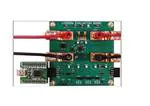
The LM25056 evaluation kit hardware is shown in Figure 2.
The board offers two connections for the system input voltage
and load. In the board's current form, the system voltage and
load can be plugged directly into the female banana receptacles. To measure higher currents, the sense resistors can be
paralleled or replaced to maintain the full-scale measurement
voltage of the sense resistor. A footprint for RS2 is not popu-
30160333
FIGURE 2. Connection Illustration
The first step to evaluate the telemetry features of LM25056
demonstration is to install the GUI software. The software is
included on a CD in the evaluation kit and is titled PMBManager-x.x.x-xxxxxxxx.exe, where the x characters indicate the
software version and build date. This file should be executed
on a PC running Windows XP or later to install the software.
Once the GUI software is installed the hardware should be
configured as shown in Figure 2
which can exceed the absolute maximum rating of the
LM25056, resulting in its destruction. To protect against such
voltage transients, a transient voltage suppression (TVS)
diode D1 is provided to clamp the voltage at the input to within
safe operating limits.
Device Evaluation
After configuring the hardware connections, apply an input
voltage of 12V to the device. The current hardware configuration allows the LM25056 device to work with 3V to 15V
system rails; however, this getting started guide will assume
an input voltage of 12V. Launch the GUI by going to the Windows Start menu -> All Programs -> PMBManager-x.xxxxx > PMBManager. A pulldown menu should come up with a list
of possible devices that the PMBManager can run. Select the
"LM25056" option as shown in Figure 3.
Hardware Setup Steps
1.
Connect the input supply to the VIN and GND banana
plugs.
2. Connect the load to the VOUT and GND banana plugs.
3. Connect the FTDI Dongle to the 10 pin connector on the
left side of the board.
4. Connect the supplied mini USB cable from the FTDI
dongle to an USB port on a PC.
When the FTDI dongle is connected for the first time the user
will be prompted to install the device drivers. For the most
current driver installation procedure refer to the
README.TXT file in the installation directory.
For testing the board functionality, a low inductance connection to the input supply is recommended. Its purpose is to
minimize voltage transients which occur when the load current changes or is shut off. If not careful, wiring inductance in
the supply lines will generate a voltage transient at shutoff
www.ti.com
30160301
FIGURE 3. Device Selector
2
�AN-2144
The device should be detected on the PMBus and the initial
load screen should appear as shown in Figure 4.
If a device is not detected, an option is provided to rescan,
ignore, or exit the GUI. If the hardware is intended to be connected, check the USB connection to the PCB, FTDI connection to the evaluation module, and verify that the power is
present on the evaluation PCB by measuring the voltage between the GND and VIN testpoints. Ignoring the detection
message allows use of the integrated design tool without the
hardware connected.
30160331
FIGURE 4. Initial GUI Screen
30160303
FIGURE 5. LM25056 Block Level Representation
Click on the detected device ID (NSC-LM25056-AA) to display a block level representation of the device as shown in
Figure 5. The block level view of the device provides a display
of all the telemetry data as well as the faults and warnings
supported by the device. The faults and warnings supported
are generally associated with an invalid input or output condition.
The warnings shown on the left side of the block representation are generally associated with the input. These include
input under voltage (UV), input over voltage (OV), and input
over power (OP). The SMBus alert status (SMBA) is also
shown on the left side and will turn red during any warning or
fault event. To facilitate the evaluation of the device, SMBus
alerts are automatically cleared by the GUI.
The warnings or faults shown on the right side of the block
representation include input over current (OC), and over temperature (OT).
The warnings shown at the bottom of the block representation
are asscociated with the VAUX measurement. The VAUX undervoltage (UV) and the VAUX overvoltage (OV) indicators
are shown next to the auxiliary measurement.
To show a repetitive update of the device telemetry and status
click on the play icon at the top of the screen. The play button
starts an active telemetry log of the gathered data. Clicking
the stop icon stops the telemetry collection and allows for the
log file to be viewed and saved. The pause button pauses both
the displaying and logging of telemetry information.
To disable displaying undesired telemetry click the display
icon on the block representation. This will open the window
shown in Figure 6 that will allow the user to disable the undesired telemetry, fault, and warning information from appearing on the block level device representation.
30160338
FIGURE 6. LM25056 Telemetry Display Options
3
www.ti.com
�AN-2144
Note that turning off the various warning options does not
mask the faults from issuing an SMBus alert - it just does not
display them if they occur. The device is capable of masking
various faults and this functionality can be setup in the device
configuration panel.
sired by left clicking on the event log window and dragging
window with the mouse to the desired location.
Plotting Telemetry
To enable telemetry data plots click on the sine wave icon
located on the LM25056 block representation. After enabling
the telemetry, a prompt will appear requesting entry of the GUI
sample rate, plot rate, and plot depth. For most cases the default rates and depths will be acceptable. The plotting tool
allows the user to select the desired data to be plotted. Up to
2 different parameters may be plotted at the same time as
shown in Figure 7.
GUI Event Log
A GUI event log is provided to keep track of GUI configuration
changes and device fault events. To display the event log select View from the main menu bar and then View Event Log.
The event log will appear in the bottom right of the main GUI
window. The event log can be detached and expanded if de-
30160335
FIGURE 7. LM25056 GUI with Telemetry Plotting Tool Enabled
Device telemetry data is plotted as a black line that continually
updates as the device is queried. In addition to the device data
the relevant warning and fault thresholds are also plotted.
Warning thresholds are shown as orange lines while fault
thresholds are shown in red.
www.ti.com
By going to the plot menu option the user can disable the
plotting grid as well as the warning and fault lines.
4
�AN-2144
Configuring the LM25056
Warning thresholds, temperature fault threshold, protection
ranges, fault masking, and averaging can be configured in the
Device Configuration panel. The first tab of this panel, shown
in Figure 8, is enabled by clicking the gear icon shown on the
LM25056 block representation.
30160360
FIGURE 9. Device Configuration Window - Fault Behavior
Tab
The Averaging tab allows the user to set the value of the
MFR_SAMPLES_FOR_AVG register of the LM25056 and
sets the number of samples averaged for telemetry of VIN,
IIN, PIN and VAUX. This is selectable from 1 to 4096 in powers of 2. Detail of the Averaging tab is shown below in Figure
10.
30160336
FIGURE 8. Device Configuration Panel - Warning and
Fault Thresholds Tab
The Warning and Fault Threshold tab allows configuration of
the input under voltage, input over voltage, output under voltage, input over current, input power, and over temperature
warnings. This tab also allows adjustment of the over temperature fault threshold. Fault threshold for the current limit
and power limit are set by the hardware design based on the
sense resistor. Decimal values for the thresholds are shown
in the text box located to the right of the slider bar. Above the
decimal values setting is the value of the setting in hexadecimal; which can be useful when developing software for this
device.
The Fault Behavior tab shown in Figure 9 allows the user to
set the device fault and warning configuration and masking.
By selecting Fault Masking, it allows individual faults and
warnings to be masked and not be shown as an SMBus alert.
Faults and warnings that only issue a SMBus alert allow
masking of the alert.
30160332
FIGURE 10. Device Configuration Window - Averaging
Tab
For convenience, the Device Configuration Panel can be undocked by holding down the left mouse button while the cursor
is at the top of the panel and dragging it to where you would
like it to be placed.
5
www.ti.com
�AN-2144
changed, the device hardware configuration needs to be updated in the design tool section. To open the design tool click
the wrench icon located on the LM25056 block representation
which will open the window displayed in Figure 11.
GUI Design Page
The GUI assumes the hardware configuration is set to default
evaluation board configuration. If any of the components are
30160337
FIGURE 11. LM25056 GUI Design Tool
Activating the design page pulls several adjustable inputs a
typical applications schematic. Design inputs are keyed in on
the left side of the window.
The input voltage for the LM25056 runs from 3 to 17V. In this
tool, it only shows the range for infomational purposes and is
not used for calculation in the remainder of the window.
The Maximum VAUX1 window is used to calculate the resistor
divider for R1 and R2. The calculator assumes that the maximum measured value of the VAUX pin is 1.0V. In operation,
the maximum measured value is near 1.2V and the difference
allows for a buffer to the full scale. The tool also assumes that
R2 is 10.0 kΩ and calculates the required R1 value. Once the
Maximum VAUX1 value is entered, Values for R1 and R2 appear in the Component Results section. The Std. 1% Resistors checkbox will enter in the closest standard 1% values that
are available to the resistors.
The Maximum Load Current window is used to determine the
size of the sense resistor needed based on the current sense
range. The LM25056 has two current sense ranges. The
GAIN=0 has an approximate current sense range of 30mV
across the sense resistor and is the default state. The GAIN=1
sets the current sense range to approximately 60mV. The
current sense range is set with the pull down window on the
left side of the design tool.
Once the Maximum Load Current and the Current Sense
Range windows are set, the current sense resistor is set in
the Current Sense Resistor and Component Results sections.
As a default, a setting of 7.5A as the maximum load current
at the current sense range of 30mV will set the current sense
resistor RS to 4 mΩ. Entering these values will also show the
www.ti.com
power dissipation of RS in the Parametric Results section at
the bottom of the design tool.
The PMBus Slave Address pulldown window shows the possible PMBus addresses that the LM25056 can be set to
respond to. By selecting the one of the 27 possible addresses,
the necessary connection to the ADR0, ADR1, and ADR2
pins is shown on the circuit diagram. As an example, if 0x17
is selected, the ADR0 would be floating, ADR1 would be connected to VDD, and ADR2 would be grounded. This set of
connections would be shown on the circuit diagram, and can
be tested on the demo board.
Once a design is complete the design should be saved by
selecting the File menu, and then Save. Once the hardware
is modified to match the design the GUI should be restarted
and the hardware configuration file loaded right after the device is detected and placed. If the values in the design tool
are different than the values on the board, erroneous telemetry and fault data will be reported by the GUI. To return to the
block view of the device press the home icon located at the
far left in the menu bar.
The design tool is also useful to calculate the PMBus coefficients. With the correct value for current sense resistor (RS1)
the tool will calculate the correct coefficients to scale the raw
telemetry data. The coefficients can be viewed by selecting
View from the main menu bar, and then selecting the PMBus
Coefficient Editor. When the PMBus Coefficient Editor is
opened, press the Get All button to show the currently used
coefficients.
If desired the equations used in the design tool can be calculated by hand using the equations provided in the datasheet.
6
�tionality of the LM25056. These features include the ability to
read telemetry, device identification and status registers, as
well monitoring the SMBus Alert interrupt.
GUI Register Page
The GUI Register Page, as shown in Figure 12, provides the
user with several features to help better understand the func-
30160362
FIGURE 12. LM25056 GUI Register Page
Telemetry is updated by clicking the Update Telemetry button. This action will update the fields under the Averaged
heading and under the Immediate heading along with PEAK
PIN. Select which parameters to update by clicking in the box
next to each parameter. If all parameter boxes under a given
heading are checked, the Update will use the block read PMBus commands (AVG_BLOCK_READ and BLOCK_READ)
to update the fields, ensuring that the readings are time
aligned. If one or more of the boxes under the headings is not
checked, the Update will use the respective individual read
PMBus commands to make the telemetry readings and the
measurements will not be time aligned. PEAK PIN is always
read with discrete PMBus commands and, therefore, are never time aligned. The CLEAR_PIN_PEAK button is provided to
clear the PEAK PIN reading which is often much higher than
one would expect under steady state conditions. This is related to the large inrush current during power-on that gets
7
www.ti.com
AN-2144
However, note the design tool calculates parameters factoring in worst case tolerances, while the equations in the
datasheet based on typical thresholds.
�AN-2144
sampled by the internal power measurement circuitry and
used to calculate PEAK PIN.
The Identification Information can be obtained by clicking the
Update ID Information button.
The rest of this page is used to monitor and diagnose warning
and fault conditions. The SMBA interrupt will indicate if a
warning or fault has occurred and if the output voltage is within
specifications. It is always active and there is no need to click
an Update button to change their state. The LM25056 does
not have a PGOOD indicator and is not used in this device.
Clicking the Update Status button under the Register Operation Control heading will update the bits in all of the registers
under the Status section as well as the telemetry in the
BLACK_BOX_READ. Clicking the CLEAR_FAULTS will reset all warning and fault bits and issue an Update Status. If
the warning and/or fault condition has been remedied, the bits
will reset. If the warning and/or fault condition still exists, the
registers will be updated within a millisecond and thus will
appear to never have been cleared. The STATUS_WORD,
STATUS_INPUT, STATUS_CML and DIAGNOSTIC_WORD
registers operate in a cumulative way. That is, these registers
display any and all warnings and errors that have occurred
since the last CLEAR_FAULTS command was issued.
The telemetry and DIAGNOSTIC_WORD that are part of the
BLACK_BOX_READ are also updated by clicking the Update
Status button. These telemetry parameters and bits are
latched at the moment the SMBA signal was asserted. They
are not reset or cleared by the CLEAR_FAULTS command
but rather they are re-armed, or readied, to be over-written
with new values at the onset of the next SMBA signal assertion. Note that these telemetry fields and this register are not
cumulative. That is, they can only be updated once after the
CLEAR_FAULTS command is issued, and it will be at the first
occurrence of the SMBA assertion following the
CLEAR_FAULTS. This allows the user to determine device
conditions at the first occurrence of the SMBA assertion.
External VDD
The LM25056 VDD can be powered from an external source
to maintain some telemetry readings if the VIN fails. On the
evaluation board, a connection of VDDX to 5V can be used
to power the VDD line and maintain telemetry readings for
VIN and temperature. The VDDX supplies power through a
Schottky diode and a large capacitor.
Note that with an external VDD connected to the VDDX line,
the LM25056 cannot be put into a low power mode with the
ENABLE pin. In this case, simply connect the ENABLE to
VDDX and lower this line down to disable the part.
Board Layout and Probing Cautions
Refer to the product datasheet for detailed layout guidelines.
For most applications the layout of this evaluation module as
detailed in the PC Board Layout section of this document
should be sufficient to provide a working solution with accurate telemetry. The following should be kept in mind when the
board is powered:
1. Use caution when probing the circuit to prevent injury as
well as possible damage to the circuit.
2. At larger load current (>15A), the wire size and length
used to connect the power source and the load may
become very important. The wires connecting this
evaluation board to the power source should be twisted
together to minimize inductance in those leads. The
same applies for the wires connecting this board to the
load. This recommendation is made in order to minimize
high voltage transients from occurring when the load
current is shut off.
3. A 15V TVS diode located as close as possible to the
LM25056 VIN and GND pins provides the critical function
of clamping inevitable input voltage overshoots when the
pass MOSFET turns off.
4. An analog signal ground plane is used local to the
LM25056 and is connected to the PCB power ground
planes at a single point.
Shutdown
With the circuit in normal operation, the LM25056 can be
shutdown by grounding the ENABLE pin.
www.ti.com
8
�FIGURE 13. Evaluation Board Schematic
30160347
AN-2144
9
www.ti.com
�AN-2144
Bill of Materials
Designator
Value
Description
Manufacturer
Part Number
Qty.
ADR0, ADR1,
ADR2
1x3
Header, TH, 100mil, 1x3, Gold plated,
230 mil above insulator
Samtec Inc.
TSW-103-07-G-S
3
C1, C4
1000pF
Ceramic, NPO, 50V, 10%, 0603
AVX
06035A102KAT2A
2
C2
0.1uF
Ceramic, X7R, 25V, 10%, 0603
AVX
06033C104KAT2A
1
C3, CREF,
CVDD
1uF
Ceramic, X7R, 16V, 10%, 0603
Murata
GRM188R71C105KA12D
3
C5
100uF
Ceramic, X5R, 6.3V, 20%, 1210
Kemet
C1210C107M9PACTU
1
D1
15V
Diode TVS 15V 5kW SMC
Littlefuse Inc.
5.0SMDJ15A
1
D2
30V, 0.2A
Diode, Schottky, SOT-23
Diodes Inc.
BAT54-7-F
1
GND2, GND3,
GND4
Test Point, TH, Miniature, Black
Keystone Electronics
5001
3
DIODE,
ENABLE,
VAUX1, VDD,
VDDX, VS+,
VS-, VREF
Test Point, TH, Miniature, White
Keystone Electronics
5002
8
VIN1, VOUT1,
GND OUT,
GND1
Terminal 90A Lug
Panduit
CB70-14-CY
4
H1, H2, H5,
H6
Screw Machine, PHIL 4-40x1/4 SS
B&F Fastener Supply
NY PMS 440 0025 PH
4
H3, H4, H7,
H8
Standoff, Hex, 4-40THR ALUM 1"L
Keystone
2205
4
J1
Male Header, 5-Pin, Dual row, Right
Angle
Samtec, Inc.
TSW-105-08-L-D-RA
1
J2
Female Header, 5-Pin, Dual row,
Right Angle
Sullins Connector
Solutions
PPPC052LJBN-RC
1
J3, J4, J5
Header, TH, 100mil, 1x2, Gold plated,
230 mil above insulator
Samtec, Inc.
TSW-102-07-G-S
3
QT1
40V, 0.2A
NPN, SOT-323
Central Semiconductor
CMPT3904
1
R1
150k
RES, 150k ohm, 1%, 0.1W, 0603
Vishay-Dale
CRCW0603150KFKEA
1
R2
10.0k
RES, 10.0k ohm, 1%, 0.1W, 0603
Vishay-Dale
CRCW060310K0FKEA
1
R4, R5, Rvs
0
RES, 0 ohm, 1%, 0.1W, 0603
Vishay-Dale
CRCW06030000Z0EA
3
Test Point, TH, Miniature, Red
Keystone Electronics
5000
4
RS+, RS-,
VIN_TP,
VOUT_TP
RES, 0.004 ohm, 1%, 3W, 3921
Vishay-Dale
WSL39214L000FEA
1
Shunt
RS1
Shunt LP w/ Handle 2 Pos 30AU,
Black
TE Connectivity
881545-2
4
Banana Jack
HDWR Banana Jack Uninsulated
Pomona Electronics
3267
4
System Power Managment IC
Vishay-Dale
LM25056APSQ
1
U1
www.ti.com
0.004 Ohm
LLP-24
10
�AN-2144
PC Board Layout
30160342
Board Top Layer
30160343
Board Mid Layer 1
11
www.ti.com
�AN-2144
30160344
Board Mid Layer 2
30160345
Board Bottom Layer (viewed from top)
www.ti.com
12
�AN-2144
Notes
13
www.ti.com
�AN-2144
LM25056 Evaluation Board
Notes
www.ti.com
�IMPORTANT NOTICE
Texas Instruments Incorporated and its subsidiaries (TI) reserve the right to make corrections, enhancements, improvements and other
changes to its semiconductor products and services per JESD46, latest issue, and to discontinue any product or service per JESD48, latest
issue. Buyers should obtain the latest relevant information before placing orders and should verify that such information is current and
complete. All semiconductor products (also referred to herein as “components”) are sold subject to TI’s terms and conditions of sale
supplied at the time of order acknowledgment.
TI warrants performance of its components to the specifications applicable at the time of sale, in accordance with the warranty in TI’s terms
and conditions of sale of semiconductor products. Testing and other quality control techniques are used to the extent TI deems necessary
to support this warranty. Except where mandated by applicable law, testing of all parameters of each component is not necessarily
performed.
TI assumes no liability for applications assistance or the design of Buyers’ products. Buyers are responsible for their products and
applications using TI components. To minimize the risks associated with Buyers’ products and applications, Buyers should provide
adequate design and operating safeguards.
TI does not warrant or represent that any license, either express or implied, is granted under any patent right, copyright, mask work right, or
other intellectual property right relating to any combination, machine, or process in which TI components or services are used. Information
published by TI regarding third-party products or services does not constitute a license to use such products or services or a warranty or
endorsement thereof. Use of such information may require a license from a third party under the patents or other intellectual property of the
third party, or a license from TI under the patents or other intellectual property of TI.
Reproduction of significant portions of TI information in TI data books or data sheets is permissible only if reproduction is without alteration
and is accompanied by all associated warranties, conditions, limitations, and notices. TI is not responsible or liable for such altered
documentation. Information of third parties may be subject to additional restrictions.
Resale of TI components or services with statements different from or beyond the parameters stated by TI for that component or service
voids all express and any implied warranties for the associated TI component or service and is an unfair and deceptive business practice.
TI is not responsible or liable for any such statements.
Buyer acknowledges and agrees that it is solely responsible for compliance with all legal, regulatory and safety-related requirements
concerning its products, and any use of TI components in its applications, notwithstanding any applications-related information or support
that may be provided by TI. Buyer represents and agrees that it has all the necessary expertise to create and implement safeguards which
anticipate dangerous consequences of failures, monitor failures and their consequences, lessen the likelihood of failures that might cause
harm and take appropriate remedial actions. Buyer will fully indemnify TI and its representatives against any damages arising out of the use
of any TI components in safety-critical applications.
In some cases, TI components may be promoted specifically to facilitate safety-related applications. With such components, TI’s goal is to
help enable customers to design and create their own end-product solutions that meet applicable functional safety standards and
requirements. Nonetheless, such components are subject to these terms.
No TI components are authorized for use in FDA Class III (or similar life-critical medical equipment) unless authorized officers of the parties
have executed a special agreement specifically governing such use.
Only those TI components which TI has specifically designated as military grade or “enhanced plastic” are designed and intended for use in
military/aerospace applications or environments. Buyer acknowledges and agrees that any military or aerospace use of TI components
which have not been so designated is solely at the Buyer's risk, and that Buyer is solely responsible for compliance with all legal and
regulatory requirements in connection with such use.
TI has specifically designated certain components as meeting ISO/TS16949 requirements, mainly for automotive use. In any case of use of
non-designated products, TI will not be responsible for any failure to meet ISO/TS16949.
Products
Applications
Audio
www.ti.com/audio
Automotive and Transportation
www.ti.com/automotive
Amplifiers
amplifier.ti.com
Communications and Telecom
www.ti.com/communications
Data Converters
dataconverter.ti.com
Computers and Peripherals
www.ti.com/computers
DLP® Products
www.dlp.com
Consumer Electronics
www.ti.com/consumer-apps
DSP
dsp.ti.com
Energy and Lighting
www.ti.com/energy
Clocks and Timers
www.ti.com/clocks
Industrial
www.ti.com/industrial
Interface
interface.ti.com
Medical
www.ti.com/medical
Logic
logic.ti.com
Security
www.ti.com/security
Power Mgmt
power.ti.com
Space, Avionics and Defense
www.ti.com/space-avionics-defense
Microcontrollers
microcontroller.ti.com
Video and Imaging
www.ti.com/video
RFID
www.ti-rfid.com
OMAP Applications Processors
www.ti.com/omap
TI E2E Community
e2e.ti.com
Wireless Connectivity
www.ti.com/wirelessconnectivity
Mailing Address: Texas Instruments, Post Office Box 655303, Dallas, Texas 75265
Copyright © 2013, Texas Instruments Incorporated
�