User's Guide
SNVA387D – February 2009 – Revised May 2013
AN-1946 LM25061 Evaluation Board
1
Introduction
The LM25061EVAL evaluation board provides the design engineer with a fully functional hot swap
controller board designed for positive voltage systems. This board contains an LM25061-2, the auto
restart version of this IC. This application note describes the various functions of the board, how to test
and evaluate it, and how to change the components for a specific application. Refer to the LM25061
Positive Low Voltage Power Limiting Hot Swap Controller (SNVS611) data sheet for more information.
The board’s specifications are:
• Input voltage range: +2.9V to 17V
• Current limit: 5 Amps, ±10%
• Q1 Power limit: 15W
• UVLO Thresholds: 4.7V and 4.45V
• PGD Thresholds: 13V and 12.5V
• Insertion delay: 213 ms
• Fault timeout period: 14.6 ms and 12.1 ms
• Restart time: 1.8 seconds
• Size: 4.0” x 1.38”
Board Configuration
R3
R1
R10
R2
U2
Z1
C8
OFF
GND VIN
LM25061 EVALUATION BD.
C2008
R8
+ C3
R9
P1
J1
Q1
C1
C5
+ C7
+ C4
R7
J2
S/N
JMP2 1
BACKPLANE
HOT SWAP CIRCUIT
PGOOD GND OUT
TP1
C6
SW1
ON
R4
2
551600159-001 REV A
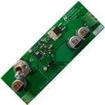
Figure 1. Evaluation Board - Top Side
A pictorial of the LM25061 evaluation board is shown in Figure 1, and the schematic is shown in Figure 2.
The “BACKPLANE” section, at the left end of the board, represents the backplane voltage source. The
vertical dashed line is the boundary between the backplane voltage source and the hot swap circuit input.
In other words, it represents the edge connector in a card cage system. The toggle switch (SW1) provides
a means to “connect” and “disconnect” the hot swap circuit from the backplane voltage source. The
All trademarks are the property of their respective owners.
SNVA387D – February 2009 – Revised May 2013
Submit Documentation Feedback
Copyright © 2009–2013, Texas Instruments Incorporated
AN-1946 LM25061 Evaluation Board
1
�Board Configuration
www.ti.com
circuitry to the right of the vertical dashed line is the hot swap circuit. The system voltage is to be
connected to the input terminal block (J1). The external load is to be connected to the output terminal
block (J2). Capacitors C3 and C4 represent capacitance which is typically present on the input of the load
circuit, and are present on this evaluation board so the turn-on characteristics of the LM25061 may be
tested without having to connect a load.
For a hot swap circuit to function reliably, capacitance is needed on the supply side of the system
connector (C7). Its purpose is to minimize voltage transients which occur whenever the load current
changes or is shut off. If the capacitance is not present, wiring inductance in the supply lines generate a
voltage transient at shutoff which can exceed the absolute maximum rating of the LM25061, resulting in its
destruction.
The LM25061EVB is supplied with pins 1-2 jumpered on JMP2.
+2.9V to +17V
VIN
J2
0.01:
S1
OUT
C7
R10
Z1
16V
GND
FDD8874
GND
Q1
C5
0.1 PF
35V
100 PF
35V
1000 pF
C1
2
VIN
R1
14k
R2
4.99k
SENSE
GATE
OUT
3
LM25061
6
0.68 PF
PWR
7
C8
3 V
PGD
R4
2.26k
UVLO/EN
PGD
BACKPLANE
1
2
FB
TIMER
PGD
JMP2
R3
23.2k
TP1
C4
220 PF
35V
9
10
1
C3
220 PF
35V
R7
100k
8
R8
0:
P1
C6
Open
GND
5
R9
34.8k
HOT SWAP CIRCUIT
LOAD
Figure 2. Evaluation Board Schematic
2
AN-1946 LM25061 Evaluation Board
SNVA387D – February 2009 – Revised May 2013
Submit Documentation Feedback
Copyright © 2009–2013, Texas Instruments Incorporated
�Theory of Operation
www.ti.com
3
Theory of Operation
The LM25061 provides intelligent control of the power supply connections of a load which is to be
connected to a live power source. The two primary functions of a hot swap circuit are in-rush current
limiting during turn-on, and monitoring of the load current for faults during normal operation. Additional
functions include Under-Voltage Lock-Out (UVLO) to ensure voltage is supplied to the load only when the
system input voltage is above a threshold, power limiting in the series pass FET (Q1) during turn-on, and
a Power Good logic output (PGD) to indicate the circuit status.
Upon applying the input voltage to the LM25061 (e.g., SW1 is switched on), Q1 is initially held off for the
insertion delay (≊213 ms) to allow ringing and transients at the input to subside. At the end of the insertion
delay, if the input voltage at VIN is above the UVLO threshold, Q1 is turned on in a controlled manner to
limit the in-rush current. If the in-rush current were not limited during turn-on, the current would be high
(very high!) as the load capacitors (C3, C4) charge up, limited only by the surge current capability of the
voltage source, C7’s characteristics, and the wiring resistance (a few milliohms). That very high current
could damage the edge connector, PC board traces, and possibly the load capacitors receiving the high
current. Additionally, the dV/dt at the load’s input is controlled to reduce possible EMI problems.
The LM25061 limits in-rush current to a safe level using a two-step process. In the first portion of the turnon cycle, when the voltage differential across Q1 is highest, Q1’s power dissipation is limited to a peak of
15W by monitoring its drain current (the voltage across R10) and its drain-to-source voltage. Their product
is maintained constant by controlling the drain current as the drain-to-source voltage decreases (as the
output voltage increases). This is shown in the constant power portion of Figure 3 where the drain current
is increasing to ILIM. When the drain currrent reaches the current limit threshold (5 Amps), it is then
maintained constant as the output voltage continues to increase. When the output voltage reaches the
input voltage (VDS decreases to near zero), the drain current then reduces to a value determined by the
load. Q1’s gate-to-source voltage then increases to its final value. The circuit is now in normal operation
mode.
Monitoring of the load current for faults during normal operation is accomplished using the current limit
circuit described above. If the load current increases to 5 Amps (50 mV across R10), Q1’s gate is
controlled to prevent the current from increasing further. When current limiting takes effect, the fault timer
limits the duration of the fault. At the end of the fault timeout period Q1 is shut off, denying current to the
load. The LM25061-2 then initiates a restart every 1.8 seconds. The restart consists of turning on Q1 and
monitoring the load current to determine if the fault is still present. After the fault is removed, the circuit
powers up to normal operation at the next restart.
In a sudden overload condition (e.g., the output is shorted to ground), it is possible the current could
increase faster than the response time of the current limit circuit. In this case, the circuit breaker sensor
shuts off Q1’s gate rapidly when the voltage across R10 reaches ≊95 mV. When the current reduces to
the current limit threshold, the current limit circuitry then takes over.
The PGD logic level output is low during turn-on, and switches high when the output voltage at OUT is
above 13V. PGD switches low when the voltage at OUT is below 12.5V. The high level voltage at PGD
can be any appropriate voltage up to +17V, and can be higher or lower than the voltages at VIN and OUT.
The UVLO thresholds are set by resistors R1 and R2 and the PGD thresholds are set by resistors R3 and
R4. Internal current sources at the UVLO pin and the FB pin provide hysteresis for the thresholds.
SNVA387D – February 2009 – Revised May 2013
Submit Documentation Feedback
Copyright © 2009–2013, Texas Instruments Incorporated
AN-1946 LM25061 Evaluation Board
3
�Board Layout and Probing Cautions
www.ti.com
VIN
VDS
Drain Current
ILIM, 5A
Constant
Power
0
12V
Gate-to- Source Voltage
VGSL
Normal
Operation
VTH
Turn-on
0
0
Figure 3. Power Up Using Power Limit and Current Limit
4
Board Layout and Probing Cautions
The pictorial in Figure 1 shows the placement of the circuit components. The following should be kept in
mind when the board is powered:
• Use CAUTION when probing the circuit to prevent injury, as well as possible damage to the circuit.
• At maximum load current (5A), the wire size and length used to connect the power source and the load
become important. The wires connecting this evaluation board to the power source SHOULD BE
TWISTED TOGETHER to minimize inductance in those leads. The same applies for the wires
connecting this board to the load. This recommendation is made in order to minimize high voltage
transients from occurring when the load current is shut off.
5
Board Connections/Startup
The input voltage source is connected to the J1 connector, and the load is connected to the J2 connector
at the OUT and GND terminals. USE TWISTED WIRES. A voltmeter should be connected to the input
terminals, and one to the output terminals. The input current can be monitored with an ammeter or current
probe. To monitor the status of the PGD output, connect a voltmeter from PGOOD to GND on the J2
terminal block. Put the toggle switch in the ON position.
Increase the input voltage gradually. The input current should remain less than 2 mA until the upper UVLO
threshold is reached. When the threshold is reached, Q1 is turned on as described in the Theory of
Operation section. If viewed on an oscilloscope, the input current increases as shown in Figure 3 before
settling at the value defined by the load. The turn-on timing depends on the input voltage, power limit
setting, current limit setting, and the final load current, and is between ≊3.0 ms with no load current, and
≊6.5 ms with a 3.7A load current, with VIN = 14V. See Figure 9 and Figure 10.
6
Circuit Parameter Changes
6.1
Current Limit
The current limit threshold is set by R10 according to the following equation:
ILIM = 50 mV/R10
(1)
If the load current increases such that the voltage across R10 reaches 50 mV, the LM25061 then
modulates Q1’s gate to limit the current to that level. This evaluation board is supplied with a 10 mohm
resistor for R10, resulting in a current limit of 5A. To change the current limit threshold replace R10 with a
resistor of the required value and power capability.
4
AN-1946 LM25061 Evaluation Board
SNVA387D – February 2009 – Revised May 2013
Submit Documentation Feedback
Copyright © 2009–2013, Texas Instruments Incorporated
�Fault Detection and Restart
www.ti.com
6.2
Power Limit
The maximum power dissipated in Q1 during turn-on, or due to a fault, is limited by R9 and R10 according
to the following equation:
PFET(LIM) =
R9
2.32 x 10⁵ x R10
(2)
With the components supplied on the evaluation board, PFET(LIM) = 15W. During turn-on, when the voltage
across Q1 is high, its gate is modulated to limit its drain current so the power dissipated in Q1 does not
exceed 15W. As the drain-to-source voltage decreases, the drain current increases, maintaining the power
dissipation constant. When the drain current reaches the current limit threshold set by R10, the current is
then maintained constant until the output voltage reaches its final value. The current then decreases to a
value determined by the load. See Figure 3, Figure 9, and Figure 10.
Each time Q1 is subjected to the maximum power limit conditions it is internally stressed for a few
milliseconds. For this reason, the power limit threshold must be set lower than the limit indicated by the
FET’s SOA chart. In this evaluation board, the power limit threshold is set at 15W, compared to ≊40W limit
indicated in the Fairchild FDD8874 data sheet. The FET manufacturer should be contacted for more
information on this subject.
6.3
Insertion Time
The insertion time starts when the input voltage at VIN reaches 2.6V, and its duration is equal to
tINSERTION = C8 x 3.13 x 105
(3)
During the insertion time, Q1 is held off regardless of the voltage at VIN. This delay allows ringing and
transients at VIN subside before the input voltage is applied to the load via Q1. The insertion time on this
evaluation board is ≊213 ms. See Figure 8.
7
Fault Detection and Restart
If the load current increases to the fault level (the current limit threshold, 5A), an internal current source
charges the timing capacitor at the TIMER pin. When the voltage at the TIMER pin reaches 1.72V, the
fault timeout period is complete, and the LM25061 shuts off Q1. The restart sequence then begins,
consisting of seven cycles at the TIMER pin between 1.72V and 1V, as shown in Figure 4. When the
voltage at the TIMER pin reaches 0.3V during the eighth high-to-low ramp, Q1 is turned on. If the fault is
still present, the fault timeout period and the restart sequence repeat.
Fault
Detection
ILIMIT
Load
Current
TIMER
Pin
20 PA
Gate Charge
2 mA
pulldown
GATE
Pin
2.5 PA
1.72V
80 PA
1V
1
2
3
7
8
0.3V
tRESTART
Fault Timeout
Period
Figure 4. Fault Timeout and Restart Sequence
The initial fault timeout period is equal to:
tFAULT(Init) = CT x 2.15 x 10⁴
(4)
The restart fault timeout period is equal to:
tFAULT(Restart) = CT x 1.776 x 10⁴
SNVA387D – February 2009 – Revised May 2013
Submit Documentation Feedback
Copyright © 2009–2013, Texas Instruments Incorporated
(5)
AN-1946 LM25061 Evaluation Board
5
�UVLO Input Voltage Threshold
www.ti.com
The restart time is equal to:
tRESTART = CT x 2.65 x 10⁶
(6)
The waveform at the TIMER pin can be monitored at the test pad located between C8 and R9. In this
evaluation board the initial fault timeout period is 14.6 ms, the restart fault timeout period is 12.1 ms, and
the restart time is 1.8 seconds. See Figure 11, Figure 12, and Figure 13.
8
UVLO Input Voltage Threshold
Programming the UVLO thresholds sets the minimum system voltage to enable the series pass device
(Q1). If VSYS is below the UVLO thresholds, Q1 is switched off, denying power to the load. Programmable
hysteresis is provided.
8.1
Option A
The UVLO thresholds are set with two resistors (R1, R2) as shown in Figure 5.
VPWR
VIN
R1
20 PA
LM25061
UVLO/
EN
1.17V
R2
TIMER AND GATE
LOGIC CONTROL
GND
Figure 5. Programming the UVLO Threshold
The two resistor values are calculated as follows:
Choose the upper and lower UVLO thresholds (VUVH) and (VUVL).
R1 =
VUVH - VUVL
VUV(HYS)
=
20 PA
20 PA
(7)
1.17V x R1
R2 =
VUVL - 1.17V
(8)
Where the resistor values are known, the threshold voltages and hysteresis are calculated from the
following:
VUVH = 1.17V + [R1 x
(1.17V + 20 PA)]
R2
(9)
1.17V x (R1 + R2)
VUVL =
R2
(10)
(11)
VUV(HYS) = R1 x 20 µA
8.2
Option B
The minimum UVLO level is obtained by connecting the UVLO pin to VIN as shown in Figure 6. On this
evaluation board the UVLO pin is accessible at the TP1 test point located to the right of the toggle switch.
Q1 is switched on when the VIN voltage reaches the POR threshold (≊2.6V).
6
AN-1946 LM25061 Evaluation Board
SNVA387D – February 2009 – Revised May 2013
Submit Documentation Feedback
Copyright © 2009–2013, Texas Instruments Incorporated
�Shutdown
www.ti.com
VPWR
VIN
20 PA
LM25061
UVLO/
EN
1.17V
TIMER AND GATE
LOGIC CONTROL
GND
Figure 6. UVLO = POR
9
Shutdown
With the circuit in normal operation, the LM25061 can be shutdown by grounding the UVLO pin. Test point
TP1, located to the right of the toggle switch, can be used for this purpose.
10
POWER GOOD and FB Pins
During turn-on, the Power Good pin (PGD) is high until the voltage at VIN increases above ≊1.6V. PGD
then switches low, remaining low as the input voltage increases. When the voltage at the board’s output
pin increases above 13V PGD switches high. PGD switches low when the output voltage decreases below
12.5V. Additionally, PGD switches low if the UVLO pin is taken below its threshold regardless of the output
voltage.
The output voltage threshold for the PGD pin is set with two resistors (R3, R4) at the FB pin as shown in
Figure 7.
Q1
SENSE
VOUT
OUT
R3
LM25061
1.17V
FB
VPGD
R4
RPG
22 PA
PGD
from UVLO
Power
Good
R8
C6
GND
Figure 7. Programming the PGD Threshold
The resistor values are calculated as follows:
- Choose the upper and lower threshold (VPGDH) and (VPGDL) at VOUT.
R3 =
VPGDH - VPGDL VPGD(HYS)
=
22 PA
22 PA
(12)
SNVA387D – February 2009 – Revised May 2013
Submit Documentation Feedback
Copyright © 2009–2013, Texas Instruments Incorporated
AN-1946 LM25061 Evaluation Board
7
�LM25061-1 Latch Version
R4 =
www.ti.com
1.17V x R3
(VPGDH - 1.17V)
(13)
Where the R3 and R4 resistor values are known, the threshold voltages and hysteresis are calculated
from the following:
VPGDH =
1.17V x (R3 + R4)
R4
(14)
(1.17V - 22 PA)]
VPGDL = 1.17V + [R3 x
R4
(15)
(16)
VPGD(HYS) = R3 x 22 µA
A pull-up voltage and pull-up resistor are required at PGD as shown in Figure 7. The pull-up voltage
(VPGD) can be as high as 17V, with transient capability to 20V, and can be higher or lower than the
voltages at VIN and OUT. This EVB is supplied with pins 1-2 jumpered on JMP2, powering the PGD pin
from the input voltage through a 100 kΩ pull-up resistor. To change the high level PGD voltage, move the
jumper on JMP2 to pins 2-3, and supply the appropriate pull-up voltage to terminal P1 (located next to
JMP2). If a delay at the PGD output is desired, a resistor and capacitor can be added at positions R8 and
C6.
11
LM25061-1 Latch Version
The LM25061-2 supplied on this evaluation board provides a restart attempt after a fault detection, as
described above. The companion Hot-Swap IC, the LM25061-1, latches off after a fault detection, with
external control required for restart. Restart is accomplished by momentarily taking the UVLO pin below its
threshold, or by removing and re-applying the input voltage at VIN. Contact the nearest Texas Instruments
sales office to obtain samples of the LM25061-1.
12
Performance Characteristics
Horizontal Resolution: 100 ms/div
Trace 1: VIN, 10V/div
Trace 2: TIMER Pin, 1V/div
Trace 3: VOUT, 10V/div
VIN = 12V, CT = 0.68 µF
Figure 8. Insertion Time Delay
8
AN-1946 LM25061 Evaluation Board
SNVA387D – February 2009 – Revised May 2013
Submit Documentation Feedback
Copyright © 2009–2013, Texas Instruments Incorporated
�Performance Characteristics
www.ti.com
Horizontal Resolution: 1 ms/div
Trace 1: PGD Pin, 10V/div
Trace 3: VOUT, 10V/div
Trace 4: Input Current, 2A/div
VIN = 14V, Load = 1 kΩ
Figure 9. Turn-On Sequence with Minimal Load Current
Horizontal Resolution: 1 ms/div
Trace 1: PGD Pin, 10V/div
Trace 3: VOUT, 10V/div
Trace 4: Input Current, 2A/div
VIN = 14V, Load = 4Ω
Figure 10. Turn-On Sequence into a 4Ω Load
Horizontal Resolution: 2 ms/div
Trace 1: PGD Pin, 10V/div
Trace 2: TIMER Pin, 1V/div
Trace 3: VOUT, 10V/div
Trace 4: Input Current, 5A/div
VIN = 14V, Load Switched from 1 kΩ to 2Ω
CT = 0.68 µF
Figure 11. Initial Fault Timeout
SNVA387D – February 2009 – Revised May 2013
Submit Documentation Feedback
Copyright © 2009–2013, Texas Instruments Incorporated
AN-1946 LM25061 Evaluation Board
9
�Performance Characteristics
www.ti.com
Horizontal Resolution: 2 ms/div
Trace 2: TIMER Pin, 1V/div
Trace 3: VOUT, 10V/div
Trace 4: Input Current, 2A/div
VIN = 14V, Load = 3Ω, CT = 0.68 µF
Figure 12. Restart Fault Timeout
Horizontal Resolution: 1sec/div
Trace 2: TIMER Pin, 1V/div
Trace 4: Input Current, 2A/div
VIN = 14V, Load = 2Ω, CT = 0.68 µF
Figure 13. Restart Timing
10
AN-1946 LM25061 Evaluation Board
SNVA387D – February 2009 – Revised May 2013
Submit Documentation Feedback
Copyright © 2009–2013, Texas Instruments Incorporated
�Bill of Materials
www.ti.com
13
Bill of Materials
Item
Description
Mfg., Part No.
Package
Value
C1
Ceramic Capacitor
TDK C2012X7R2A102M
0805
1000 pF, 100V
C3, C4
Alum. Elec. Capacitor
Panasonic EEE-TG1V221UP
Surf. Mount
220 µF, 35V
C5
Ceramic Capacitor
TDK C3216X7R2A104M
1206
0.1 µF, 100V
C6
Unpopulated
C7
Alum. Elec. Capacitor
Panasonic EEE-TG1V101P
Surf. Mount
100 µF, 35V
C8
Ceramic Capacitor
MuRata GRM188R61A684KA61D or
Panasonic ECJ-2FB1A684K
0805
0.68 µF, 10V or higher
Q1
MOSFET
Fairchild FDD8874
TO-252
R1
Resistor
Vishay CRCW120614K0F
1206
14k
R2
Resistor
Vishay CRCW08054K99F
0805
4.99k
R3
Resistor
Vishay CRCW080523K2F
0805
23.2k
R4
Resistor
Vishay CRCW08052K26F
0805
2.26k
R7
Resistor
Vishay CRCW1206100KF
1206
100k, ¼ W
R8
Resistor
Vishay CRCW08050000Z
0805
Zero ohm jumper
R9
Resistor
Vishay CRCW080534K8F
0805
34.8k
R10
Resistor
Vishay WSL2010R0100F
2010
0.010 ohm, ½ W
SW1
Toggle Switch
NKK M2012SS1W03-RO
U2
Hot Swap IC
Texas Instruments LM25061
VSSOP-10
Z1
Trans. Suppressor
Diodes Inc. SMBJ16A
SMB
SNVA387D – February 2009 – Revised May 2013
Submit Documentation Feedback
Copyright © 2009–2013, Texas Instruments Incorporated
SPDT switch, 6A
16V
AN-1946 LM25061 Evaluation Board
11
�PC Board Layout
14
www.ti.com
PC Board Layout
Figure 14. Board Silkscreen
Figure 15. Board Top Layer
Figure 16. Board Bottom Layer (viewed from top)
12
AN-1946 LM25061 Evaluation Board
SNVA387D – February 2009 – Revised May 2013
Submit Documentation Feedback
Copyright © 2009–2013, Texas Instruments Incorporated
�IMPORTANT NOTICE
Texas Instruments Incorporated and its subsidiaries (TI) reserve the right to make corrections, enhancements, improvements and other
changes to its semiconductor products and services per JESD46, latest issue, and to discontinue any product or service per JESD48, latest
issue. Buyers should obtain the latest relevant information before placing orders and should verify that such information is current and
complete. All semiconductor products (also referred to herein as “components”) are sold subject to TI’s terms and conditions of sale
supplied at the time of order acknowledgment.
TI warrants performance of its components to the specifications applicable at the time of sale, in accordance with the warranty in TI’s terms
and conditions of sale of semiconductor products. Testing and other quality control techniques are used to the extent TI deems necessary
to support this warranty. Except where mandated by applicable law, testing of all parameters of each component is not necessarily
performed.
TI assumes no liability for applications assistance or the design of Buyers’ products. Buyers are responsible for their products and
applications using TI components. To minimize the risks associated with Buyers’ products and applications, Buyers should provide
adequate design and operating safeguards.
TI does not warrant or represent that any license, either express or implied, is granted under any patent right, copyright, mask work right, or
other intellectual property right relating to any combination, machine, or process in which TI components or services are used. Information
published by TI regarding third-party products or services does not constitute a license to use such products or services or a warranty or
endorsement thereof. Use of such information may require a license from a third party under the patents or other intellectual property of the
third party, or a license from TI under the patents or other intellectual property of TI.
Reproduction of significant portions of TI information in TI data books or data sheets is permissible only if reproduction is without alteration
and is accompanied by all associated warranties, conditions, limitations, and notices. TI is not responsible or liable for such altered
documentation. Information of third parties may be subject to additional restrictions.
Resale of TI components or services with statements different from or beyond the parameters stated by TI for that component or service
voids all express and any implied warranties for the associated TI component or service and is an unfair and deceptive business practice.
TI is not responsible or liable for any such statements.
Buyer acknowledges and agrees that it is solely responsible for compliance with all legal, regulatory and safety-related requirements
concerning its products, and any use of TI components in its applications, notwithstanding any applications-related information or support
that may be provided by TI. Buyer represents and agrees that it has all the necessary expertise to create and implement safeguards which
anticipate dangerous consequences of failures, monitor failures and their consequences, lessen the likelihood of failures that might cause
harm and take appropriate remedial actions. Buyer will fully indemnify TI and its representatives against any damages arising out of the use
of any TI components in safety-critical applications.
In some cases, TI components may be promoted specifically to facilitate safety-related applications. With such components, TI’s goal is to
help enable customers to design and create their own end-product solutions that meet applicable functional safety standards and
requirements. Nonetheless, such components are subject to these terms.
No TI components are authorized for use in FDA Class III (or similar life-critical medical equipment) unless authorized officers of the parties
have executed a special agreement specifically governing such use.
Only those TI components which TI has specifically designated as military grade or “enhanced plastic” are designed and intended for use in
military/aerospace applications or environments. Buyer acknowledges and agrees that any military or aerospace use of TI components
which have not been so designated is solely at the Buyer's risk, and that Buyer is solely responsible for compliance with all legal and
regulatory requirements in connection with such use.
TI has specifically designated certain components as meeting ISO/TS16949 requirements, mainly for automotive use. In any case of use of
non-designated products, TI will not be responsible for any failure to meet ISO/TS16949.
Products
Applications
Audio
www.ti.com/audio
Automotive and Transportation
www.ti.com/automotive
Amplifiers
amplifier.ti.com
Communications and Telecom
www.ti.com/communications
Data Converters
dataconverter.ti.com
Computers and Peripherals
www.ti.com/computers
DLP® Products
www.dlp.com
Consumer Electronics
www.ti.com/consumer-apps
DSP
dsp.ti.com
Energy and Lighting
www.ti.com/energy
Clocks and Timers
www.ti.com/clocks
Industrial
www.ti.com/industrial
Interface
interface.ti.com
Medical
www.ti.com/medical
Logic
logic.ti.com
Security
www.ti.com/security
Power Mgmt
power.ti.com
Space, Avionics and Defense
www.ti.com/space-avionics-defense
Microcontrollers
microcontroller.ti.com
Video and Imaging
www.ti.com/video
RFID
www.ti-rfid.com
OMAP Applications Processors
www.ti.com/omap
TI E2E Community
e2e.ti.com
Wireless Connectivity
www.ti.com/wirelessconnectivity
Mailing Address: Texas Instruments, Post Office Box 655303, Dallas, Texas 75265
Copyright © 2013, Texas Instruments Incorporated
�