User's Guide
SNVA464C – December 2010 – Revised April 2013
AN-2100 LM25066 Evaluation Board
1
Introduction
The LM25066EVK evaluation kit provides the design engineer with a fully functional, intelligent monitoring
and hot-swap protection board designed for positive voltage systems. This application note describes the
various functions of the evaluation board, how to test and evaluate it, and how to use the companion GUI.
The GUI is used to collect telemetry, configure warning and fault thresholds, and assist the designer with
selection of the external components for a specific application. Use of the advanced telemetry and
monitoring capabilities of the LM25066 requires external control via the Power Management Bus (PMBus)
interface. However, the LM25066 is capable of acting as a hot-swap and protection circuit without any
PMBus intervention. Please check the LM25066 System Power Management & Protection IC with PMBus
(SNVS654) data sheet for the latest software and data sheet information.
2
PCB Features
•
•
•
•
•
•
•
•
•
•
Input voltage range: 2.9V to 16V (limited by input clamp D1)
Programmable current limit: set to 50A (±8%)
Q1 power limit: 80W (typical)
UVLO thresholds: 2.9V and 3.1V
PGD thresholds: 10.8V and 10.25V
Insertion delay: 147 ms (typical)
Fault time-out period: 8.9 ms
Restart time: 1.1 seconds
PCB size: 3.5” x 4.2”
Solution size: 0.7” x 0.7”
Panduit is a registered trademark of Panduit Corp.
All other trademarks are the property of their respective owners.
SNVA464C – December 2010 – Revised April 2013
Submit Documentation Feedback
Copyright © 2010–2013, Texas Instruments Incorporated
AN-2100 LM25066 Evaluation Board
1
�Simplified Schematic
3
www.ti.com
Simplified Schematic
RS+
VIN
1 PF
1
2
ADR0
R1
10k
CB
1
2
CB
3
3
R3
49.9k
17
ADR1
CLIM
1
2
1
2
ADR1
CLIM
R4
4.12k
3
3
VDD
VDD
RETRY
ADR2
1
2
ADR2
RETRY
3
TM
9
PMBus
CT
0.47 PF
Connectors
J1
1
3
5
7
9
13
GATE
12
RFB2
2.74k
VAUX
C4
1 nF
LM25066
DIODE
23
6
C3
CB
CB
5
CLIM 1 nF
CL
RETRY 8 RETRY
PGD 11
VDD
4
CVDD
4.7 PF
R5
150k
24
OVLO
TIMER VREF GND
22
18
C6
C5
330 PF 330 PF
25V
25V
VAUX
7
FB
CREF
1 PF
GND
RFB1
22.6k
OUT
UVLO/EN
19
SDA
SDA
20
SCL
SCL
SMBA 21 SMBA
3
ADR0
ADR0
2
ADR1
ADR1
1
ADR2
ADR2
1
2
3
14
SENSE
R2
6.81k
VDD
VDD
VIN
16
D2
C2
0.1 PF
25V
15
VDD
ADR0
Q1
CIN
JUMPERS
VDD
VOUT
PSMN1R2-25YL
RS1
D1
15V
GND
SCL
SDA
SMBA
RS-
0.5 m:
R6
10k
CMPT3904
(Near Q1)
QT
VDD
RPG
PGD
10k
PWR
10
RPWR
6.98k
J2
2
4
6
8
10
GND
SCL
SDA
SMBA
PGOOD
GND
1
3
5
7
9
2
4
6
8
10
GND
PGOOD
GND
Figure 1. Simplified Evaluation Board Schematic
The simplified schematic for the LM25066 evaluation board is shown in Figure 1. Connections to the
PMBus interface are provided by connector J1. Panduit® terminal lugs bolt down to the PCB to provide
input and output connections. Jumpers ADR0, ADR1, and ADR2 set the PMBus slave address of the
LM25066 to one of 27 unique addresses. Jumpers also exist to set the retry, circuit breaker, and current
limit behavior. Test points are provided for VIN, VOUT, GATE, UVLO, VAUX, PGD, VREF, TIMER and
GND.
4
Getting Started
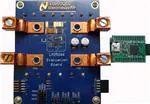
The LM25066 evaluation kit hardware is shown in Figure 2. The board offers two connection methods for
the system input voltage and load. For evaluation at currents below 15A, the system voltage and load can
be plugged directly into the female banana receptacles. For higher currents, it is recommended to use the
copper Panduit lugs with low gauge wire to minimize the cable power dissipation and voltage drop.
Capacitors C5 and C6 represent capacitance which is typically present at the input of the load circuit and
are present on this evaluation board so that the turn-on characteristics of the LM25066 may be tested
starting into a capacitive load. Footprints for components RS2 and Q2 are not populated and are provided
to accommodate evaluation of hot-swap designs with current levels greater than 50A.
The LM25066EVK is supplied with the PMBus slave address set to 0x16 as dictated by the configuration
of the ADR0, ADR1, and ADR2 jumper connections.
2
AN-2100 LM25066 Evaluation Board
SNVA464C – December 2010 – Revised April 2013
Submit Documentation Feedback
Copyright © 2010–2013, Texas Instruments Incorporated
�Hardware Setup Steps
www.ti.com
Figure 2. Connection Illustration
The first step to evaluate the telemetry features of the LM25066 is to install the GUI application. The
application distribution is included on a CD in the evaluation kit and is titled PMBManager-x.x.xxxxxxxxx.exe, where the x characters indicate the software version and build date. To install the
application, this file should be executed on a PC running Windows XP or later. Once the application is
installed, the hardware should be connected as shown in Figure 2.
5
Hardware Setup Steps
1. Connect the input supply to either the VIN and GND banana plugs (IOUT15A).
2. Connect the load to either the VOUT and GND banana plugs (IOUT15A).
3. Connect the FTDI Dongle to the 10-pin connector on the left side of the board.
4. Connect the supplied mini USB cable from the FTDI dongle to a USB port on a PC.
When the FTDI dongle is connected for the first time, the user will be prompted to install the device
drivers. For the most recent driver installation procedure, please refer to the README.TXT file in the
installation directory.
For a hot-swap circuit to function reliably, a low inductance connection to the input supply is
recommended. Its purpose is to minimize voltage transients which occur when the load current changes or
is shut off. High parasitic inductance in the supply lines coupled with the rapid change of current when the
FET turns off will induce a voltage spike. This spike can exceed the absolute maximum voltage rating of
the LM25066, resulting in its destruction. To protect against such voltage spikes, TVS diode D1 is
provided to clamp the input voltage to within safe operating limits. Likewise, Schottky diode D2 is provided
at the output to clamp the output voltage from going too negative during short circuit events.
6
GUI Evaluation
After the hardware connections have been made, apply an input voltage of 12V. The current hardware
configuration allows the LM25066 to work with 3.3V, 5.0V, and 12V system rails. However, this Quick
Start guide will assume an input voltage of 12V. From the Windows Start menu, launch the GUI
application. The LM25066 should be detected on the PMBus and an initial screen should appear as
shown in Figure 3.
SNVA464C – December 2010 – Revised April 2013
Submit Documentation Feedback
Copyright © 2010–2013, Texas Instruments Incorporated
AN-2100 LM25066 Evaluation Board
3
�GUI Evaluation
www.ti.com
Figure 3. Initial GUI Screen
If the LM25066 is not detected, an option is provided to rescan, ignore, or exit the GUI. If the hardware is
intended to be connected, check the USB connection to the PC, the FTDI connection to the evaluation
board, and verify that the power is present on the evaluation board by measuring the voltage between the
VIN and GND testpoints. Choosing the Ignore option causes the application to bypass additional attempts
to detect the LM25066 on the PMBus and facilitates access to the GUI integrated design tool.
Single-click on the detected device ID, NSC-LM25066-AA, to display a block level representation as
shown in Figure 4. The block level view of the device provides a display of all the telemetry as well as
most of the faults and warnings supported by the LM25066. The faults and warnings supported are
generally associated with an invalid input or output condition.
Figure 4. LM25066 Block Level Representation
The faults shown on the left side of the block representation are generally associated with the input. The
faults include input under-voltage (UV), input over-voltage (OV), FET Fail (FF), and input over-power (OP).
The SMBus alert status, SMBA, is also shown on the left side and will turn red during any warning or fault
event. To facilitate evaluation of the LM25066, SMBus alerts are automatically cleared by the GUI while
telemetry is monitored.
The faults shown on the right side of the block representation are associated with the output. These
include output under-voltage (UV), power good status (PGD), output over-current (OC), and overtemperature (OT). There is also an indicator if the output is in the latched-off state (LO). The LM25066 will
latch the output off after the number of programmed retries is exceeded. To clear the latched-off condition,
the output can be toggled off and then on by the red Power button located at the top right of the LM25066
block representation.
4
AN-2100 LM25066 Evaluation Board
SNVA464C – December 2010 – Revised April 2013
Submit Documentation Feedback
Copyright © 2010–2013, Texas Instruments Incorporated
�GUI Event Log
www.ti.com
To show a continuuous update of the LM25066 telemetry and status, click on the Play button at the top of
the screen. The Play button starts an active telemetry log of the gathered data. Clicking the Stop button
stops the telemetry collection and allows the log file to be viewed and saved. The Pause button pauses
both the displaying and logging of telemetry information, but does not clear the log.
To enable/disable display of specific telemetry, click the Display Options button on the block
representation and choose the desired telemetry to display (see Figure 5).
Figure 5. LM25066 Telemetry Display Options
Note that enabling/disabling the various warning and fault options has no affect on the Fault mask.
7
GUI Event Log
A GUI Event Log is provided to keep track of GUI configuration changes and LM25066 fault events. To
display the Event Log, select View from the main menu bar and then View Event Log. The dockable
window housing the Event Log can be detached (or docked to a different region of the GUI) by dragging
its title bar to the desired location.
8
Plotting Telemetry
To enable telemetry data plots, click on the Device Telemetry (sinewave) button located in the LM25066
block representation. After enabling the telemetry, a prompt will appear requesting entry of the GUI
sample rate, plot rate, and plot depth. For most cases, the default rates and depths will be acceptable.
The plotting tool allows the user to select the desired data to be plotted. Up to two different parameters
may be plotted simultaneously, as shown in Figure 6.
SNVA464C – December 2010 – Revised April 2013
Submit Documentation Feedback
Copyright © 2010–2013, Texas Instruments Incorporated
AN-2100 LM25066 Evaluation Board
5
�Configuring the LM25066
www.ti.com
Figure 6. LM25066 GUI with Telemetry Plotting Tool Enabled
Telemetry is plotted as a black line that continually updates as the LM25066 is queried. In addition to the
telemetry, the relevant warning and fault thresholds are also plotted. Warning thresholds are shown as
orange lines while fault thresholds are shown in red and blue.
From the Plot menu option in the main menu bar, the user can disable the plotting grid as well as the
warning and fault lines.
9
Configuring the LM25066
Warning Thresholds, Temperature Fault Threshold, Protection Ranges, Fault Masking, and Averaging can
be configured in the Device Configuration panel. This panel, shown in Figure 7, is enabled by clicking the
Gear button shown in the LM25066 block representation.
6
AN-2100 LM25066 Evaluation Board
SNVA464C – December 2010 – Revised April 2013
Submit Documentation Feedback
Copyright © 2010–2013, Texas Instruments Incorporated
�Configuring the LM25066
www.ti.com
Figure 7. Device Configuration Panel - Warning and Fault Thresholds Tab
The Warning and Fault Thresholds tab allows configuration of the input under-voltage, input over-voltage,
output under-voltage, input over-current, input power, and over-temperature warnings. This tab also allows
adjustment of the over-temperature fault threshold. Adjustments can be made by moving the slider button
with the mouse, by clicking on the slider line, or by clicking on the up/down arrows in the number box.
Fault thresholds for the input under- and over-voltage, current limit, power limit, and power good are set by
external configuration components. Decimal values for the thresholds are shown in the text box located to
the right of the slider bar. Above the decimal values setting is the value of the setting in hexadecimal; this
can be useful when developing software/firmware to control and configure the LM25066.
The Fault Behavior tab, shown in Figure 8, allows the user to set the LM25066 fault configuration and fault
masking. The fault configuration section allows the user to set the number of retries, as well as the circuit
breaker and current limit thresholds. The number of retries is set by the RETRY pin at power-on-reset
(POR) to be infinite or latched-off. Subsequently, the number of retries can be set via the PMBus interface
to 0 (latch-off), 1, 2, 4, 8, 16 or infinite. The software settings are independent of the hardware settings.
However, if the power is cycled, the LM25066 will default to the setting based on the RETRY pin. Current
limit and circuit breaker power-up settings are set by the CL and CB pins, respectively. The current limit
threshold can be set to either 25 mV (CL = GND) or 46 mV (CL = VDD). The circuit breaker threshold can
also be set to either 1.8 times (CB = GND) or 3.6 times (CB = VDD) the current limit threshold. Fault
SNVA464C – December 2010 – Revised April 2013
Submit Documentation Feedback
Copyright © 2010–2013, Texas Instruments Incorporated
AN-2100 LM25066 Evaluation Board
7
�GUI Design Page
www.ti.com
masking is possible for many of the LM25066 fault conditions. Fault conditions allow masking of both the
MOSFET response and the SMBus alert signal. Note that if a fault persists while the MOSFET gate
masking is enabled, damage to the MOSFET may occur. This option is allowed primarily for debug
purposes. Faults that issue only a SMBus alert (FET Fail, Communications Fault) allow masking of the
alert. Note that the power-up default setting for the Power Good signal is to mask the SMBus alert.
Figure 8. Device Configuration Panel - Fault Behavior Tab
For convenience, the dockable window containing the Device Configuration tabs can be detached (or
docked to a different region of the GUI) by dragging its title bar to the desired location.
10
GUI Design Page
The GUI assumes the hardware configuration is set to the default LM25066 evaluation board
configuration. If any of the components are changed, the LM25066 hardware configuration needs to be
updated in the Design Tool section. To open the design tool, click the Wrench button located in the
LM25066 block representation which will display the window as shown in Figure 9.
8
AN-2100 LM25066 Evaluation Board
SNVA464C – December 2010 – Revised April 2013
Submit Documentation Feedback
Copyright © 2010–2013, Texas Instruments Incorporated
�GUI Design Page
www.ti.com
Figure 9. LM25066 Design Tool
Design inputs are keyed in on the left side following steps 1 though 5. General operating conditions should
be entered in step 1 of the design tool. These inputs help set bounds on the startup time and application
voltage and current ranges.
Step 2 allows the user to tailor the MOSFET protection features specific to the target application. Both pin
and software configurable ranges are available for the circuit breaker and current limit circuits. If a pin
configuration is selected, please make sure the CB and CL jumpers are set to match the GUI selection.
Note that the state of all jumpers is sampled only at startup (POR). Thus, if any changes are made to the
jumpers, be sure to cycle power. By clicking on the MOSFET SOA Profile button, the user can select SOA
data from several popular MOSFETs or enter the SOA data for the desired MOSFET.
Step 3 allows the user to select the under- and over-voltage lockout (UVLO/OVLO) levels, and power
good (PGD) thresholds. Note that with the correct values for R1 - R4, and RFB1 and RFB2 installed, the
LM25066 will indicate a fault condition when the input and/or output voltages are outside of their
respective ranges.
Step 4 allows the user to set the fault timeout period and the fault response. The fault timeout should be
set to be below the MOSFET SOA data for a given time. For example, if a design is to adhere to the 10
ms pulsed MOSFET SOA data, the desired fault timeout must be less than 10 ms. The fault timeout time
entered will set the value for CT. It also sets the insertion delay and fault retry delay. The initial power up
retry behavior is also selected in this design step. Make sure to change the RETRY jumper to match the
design tool schematic when changing the default retry setting.
SNVA464C – December 2010 – Revised April 2013
Submit Documentation Feedback
Copyright © 2010–2013, Texas Instruments Incorporated
AN-2100 LM25066 Evaluation Board
9
�GUI Register Page
www.ti.com
In Step 5, the user enters the desired PMBus slave address. Note that changing the PMBus slave address
in this step does not change the physical address, but shows how the address pins of the LM25066 need
to be configured to achieve a desired address. Once the ADR pin jumpers are configured for a particular
address, power to the LM25066 needs to be cycled and the GUI restarted in order for the new address to
take effect.
When invalid or incorrect inputs are given to the design tool, text associated with the faulty input will turn
red. Positioning the mouse cursor over the red text will give additional information about any design
conflict.
Component and parametric results are shown to the right as well as the LM25066 operational area chart.
The operational area chart shows the minimum, typical, and maximum SOA protection areas for a given
design. For a robust design, the SOA of the MOSFET used should be above the MAX protection SOA line
for all operating areas. To help make this determination, step 2 allows the user to select the SOA curves
for several popular MOSFETs or to input the SOA data for the desired MOSFET.
Once complete, the design should be saved by selecting the File menu, and then Save. Once the
hardware is modified to match the design, the GUI should be restarted and the hardware configuration file
loaded right after the LM25066 is detected and placed. If the values in the design tool are different than
the values on the board, erroneous telemetry and fault data will be reported by the GUI. To return to the
block view of the device, press the Home button located at the far left in the menu bar.
The design tool is also useful to calculate the PMBus coefficients. With the correct value for current sense
resistor (RS1), the tool will calculate the coefficients to scale the raw telemetry. The coefficients can be
viewed by selecting View from the main menu bar, and then selecting the PMBus Coefficient Editor. When
the PMBus Coefficient Editor is opened, press the Get All button to show the currently used coefficients.
If desired, the equations used in the design tool can be calculated by hand using the equations provided in
the datasheet. However, note that the design tool calculates parameters factoring in worst case
tolerances, while the equations in the datasheet are based on typical thresholds.
11
GUI Register Page
The GUI Register Page, as shown in Figure 10, provides the user with several features to help better
understand the functionality of the LM25066. These features include the ability to read telemetry, device
identification and status registers, as well as being able to monitor the SMBus Alert and PGOOD
interrupts, and to turn the output on and off with the OPERATION button.
10
AN-2100 LM25066 Evaluation Board
SNVA464C – December 2010 – Revised April 2013
Submit Documentation Feedback
Copyright © 2010–2013, Texas Instruments Incorporated
�GUI Register Page
www.ti.com
Figure 10. LM25066 GUI Register Page
Telemetry is updated by clicking the Update Telemetry button. This action will update the fields under the
Averaged heading and under the Immediate heading along with VAUX and PEAK PIN. Select which
parameters to update by clicking in the box next to each parameter. If all parameter boxes under a given
heading are checked, the Update will use the block read PMBus commands (AVG_BLOCK_READ and
BLOCK_READ) to update the fields, ensuring that the readings are time aligned. If one or more of the
boxes under the headings is not checked, the Update will use the respective individual read PMBus
commands to make the telemetry readings and the measurements will not be time aligned. VAUX and
PEAK PIN are always read with discrete PMBus commands and, therefore, are never time aligned. The
CLEAR_PIN_PEAK button is provided to clear the PEAK PIN reading which is often much higher than one
would expect under steady state conditions. This is related to the large inrush current during power-on that
gets sampled by the internal power measurement circuitry and used to calculate PEAK PIN.
The output can be turned off and on using the OPERATION button, and the Identification Information can
be obtained by clicking the Update ID Information button.
The rest of this page is used to monitor and diagnose warning and fault conditions. The SMBA and
PGOOD interrupts will indicate if a warning or fault has occurred and if the output voltage is within
specifications. They are always active and there is no need to click an Update button to change their
state. Clicking the Update Status button under the Register Operation Control heading will update the bits
in all of the registers, as well as the telemetry, under the Status section. Clicking the CLEAR_FAULTS will
reset all warning and fault bits and issue an Update Status. If the warning and/or fault condition has been
remedied, the bits will reset. If the warning and/or fault condition still exists, the registers will be updated
within a millisecond and thus will appear to never have been cleared. The STATUS_WORD,
STATUS_INPUT, STATUS_CML and DIAGNOSTIC_WORD registers operate in a cumulative way. That
is, these registers display any and all warnings and errors that have occurred since the last
CLEAR_FAULTS command was issued.
SNVA464C – December 2010 – Revised April 2013
Submit Documentation Feedback
Copyright © 2010–2013, Texas Instruments Incorporated
AN-2100 LM25066 Evaluation Board
11
�Theory of Operation
www.ti.com
The telemetry and DIAGNOSTIC_WORD that are part of the BLACK_BOX_READ are also updated by
clicking the Update Status button. These telemetry parameters and bits are latched at the moment the
SMBA signal was asserted. They are not reset or cleared by the CLEAR_FAULTS command but rather,
they are re-armed, or readied, to be over-written with new values at the onset of the next SMBA signal
assertion. Note that these telemetry fields and this register are not cumulative. That is, they can only be
updated once after the CLEAR_FAULTS command is issued, and it will be at the first occurrence of the
SMBA assertion following the CLEAR_FAULTS. This allows the user to determine device conditions at the
first occurrence of the SMBA assertion.
12
Theory of Operation
The LM25066 provides intelligent control of the power supply connections of a load which is to be
connected to a live power source. The three primary functions of the LM25066 are to limit inrush current
during turn-on, respond to warnings and faults, and to provide system telemetry for the following
parameters: Input Voltage (VIN), Input Current (IIN), Input Power (PIN), Output Voltage (VOUT), Auxilliary
Voltage (VAUX), and Temperature. Additional functions include under- and over-voltage lockouts
(UVLO/OVLO) to ensure voltage is supplied to the load only when the system input voltage is within a
specified range, power limiting of the series pass MOSFET (Q1) during turn-on, and a Power Good logic
output (PGD) to indicate the output voltage status.
Upon applying the input voltage to the LM25066, Q1 is initially held off for the insertion delay (≊147 ms) to
allow ringing and transients on the input to subside. At the end of the insertion delay, if the input voltage
and temperature are within acceptable limits, Q1 is turned on in a controlled manner to limit the inrush
current. If the inrush current were not limited during turn-on, the current would be high as the load
capacitors (C5 and C6) charge up, limited only by the surge current capability of the voltage source, the
capacitor characteristics, and the wiring resistance (a few milliohms). That very high current could damage
the edge connector, PC board traces, and possibly the load capacitors receiving the high current.
Additionally, the dV/dt at the load’s input is controlled to reduce possible EMI problems.
The LM25066 limits inrush current to a safe level using a two step process. In the first portion of the turnon cycle, when the voltage differential across Q1 is highest, Q1’s power dissipation is limited to a peak
value (80W typically, set by RPWR) by monitoring its drain current (the voltage across shunt RS1) and its
drain-to-source voltage. Their product is maintained constant by controlling the drain current as the drainto-source voltage decreases (corresponding to an increasing output voltage). This is shown in the
constant power portion of Figure 11 where the drain current is increasing to ILIM. When the drain current
reaches the current limit threshold (50A), it is then maintained constant as the output voltage continues to
increase. When the output voltage reaches the input voltage level (VDS decreases to near zero), the drain
current then reduces to a value determined by the load. Q1’s gate-to-source voltage then increases to its
final value. The circuit is now in normal operation mode.
Monitoring of the load current for faults during normal operation is accomplished using the current limit
circuit described above. If the load current increases to 50A (25 mV across RS1), Q1’s gate is controlled
to prevent the current from increasing further. When current limiting takes effect, the fault timer limits the
duration of the fault. At the end of the fault time-out period, Q1 is shut off, denying current to the load. The
LM25066 then initiates a restart every 1.1 seconds. The restart consists of turning on Q1 and monitoring
the load current to determine if the fault is still present. After the fault is removed, the circuit powers up to
normal operation at the next restart.
In a sudden overload condition (when the output is shorted to ground), it is possible that the current could
increase faster than the response time of the current limit circuit. In this case, the circuit breaker feature
shuts off Q1’s gate rapidly when the voltage across RS1 reaches 45 mV. When the current reduces to the
current limit threshold, the current limit circuitry then takes over.
The PGD logic level output is low during turn-on and switches high when the output voltage at VOUT is
above 10.8V. PGD switches low when the voltage at VOUT is below 10.25V. The high level voltage at
PGD can be any appropriate voltage up to 17V and can be higher or lower than the voltages at VIN and
OUT.
The UVLO thresholds are set by resistors R1 and R2, the OVLO thresholds are set by R3 and R4, and the
PGD thresholds are set by resistors RFB1 and RFB2. Internal current sources at the UVLO, OVLO, and
FB pins provide hysteresis for these thresholds.
12
AN-2100 LM25066 Evaluation Board
SNVA464C – December 2010 – Revised April 2013
Submit Documentation Feedback
Copyright © 2010–2013, Texas Instruments Incorporated
�Fault Detection and Restart
www.ti.com
VIN
VDS
Drain Current
ILIM
Constant
Power
0
12V
Gate-to- Source Voltage
VGSL
Normal
Operation
VTH
Turn-on
0
0
Figure 11. Power Up Using Power Limit and Current Limit
13
Fault Detection and Restart
If the load current increases to the fault level (the current limit threshold of 50A), an internal current source
charges the timing capacitor at the TIMER pin. When the voltage at the TIMER pin reaches 1.7V, the fault
time-out period is complete and the LM25066 shuts off Q1. The restart sequence then begins, consisting
of seven cycles at the TIMER pin between 1.7V and 1V, as shown in Figure 12. When the voltage at the
TIMER pin reaches 0.3V during the eighth high-to-low ramp, Q1 is turned on. If the fault is still present, the
fault time-out period and the restart sequence repeat.
Fault
Detection
ILIMIT
Load
Current
22 PA
Gate Charge
2 mA pulldown
GATE
Pin
2.8 PA
1.7V
90 PA
TIMER
Pin
1V
1
2
3
7
8
0.3V
t RESTART
Fault Timeout
Period
Figure 12. Fault Time-out and Restart Sequence
The waveform at the TIMER pin can be monitored at the TIMER test point. On this evaluation board, the
initial fault time-out period is 8.9 ms and the restart time is 1.1 seconds. See Figure 18.
14
UVLO and OVLO Input Voltage Threshold
Programming the UVLO thresholds sets the minimum system voltage to enable the series pass MOSFET
(Q1). If VIN is below the UVLO thresholds, Q1 is switched off, denying power to the load. Programmable
hysteresis is adjustable by changing the value of R1.
The UVLO thresholds are set with two resistors (R1, R2) as shown in Figure 13.
SNVA464C – December 2010 – Revised April 2013
Submit Documentation Feedback
Copyright © 2010–2013, Texas Instruments Incorporated
AN-2100 LM25066 Evaluation Board
13
�POWER GOOD and FB Pins
www.ti.com
The OVLO threshold sets the maximum voltage that can be present on the input before the LM25066
turns off the series pass MOSFET. The OVLO threshold is set with the two resistors (R3, R4). The
hysteresis voltage is set by the internal 23 µA current source and the value of R3.
VSYS
VIN
23PA
R1
UVLO/EN
1.16V
TIMER AND
GATE
LOGIC CONTROL
R2
R3
1.16V
OVLO
R4
LM25066
23PA
GND
Figure 13. Programming the UVLO Threshold
15
POWER GOOD and FB Pins
During turn-on, the Power Good pin (PGD) will not be able to pull low until the voltage at VIN increases
above ≊1.6V. Using VDD as the pull-up voltage source will keep the PGD pin low during this region
because VDD does not turn on until VIN increases above ≊2.5V. When the voltage at the board’s output
pin increases above 10.8V (typ), PGD switches high. PGD switches low when the output voltage
decreases below 10.25V (typ). Additionally, PGD switches low if the UVLO/EN pin is taken below its
threshold regardless of the output voltage.
The output voltage threshold for the PGD pin is set with two resistors (RFB1, RFB2) at the FB pin.
Q1
SENSE
VOUT
OUT
RFB1
LM25066
1.167V
FB
VDD
RFB2
RPG
24 PA
Power
Good
PGD
OVLO
UVLO
GND
Figure 14. Programming the PGD Threshold
A pull-up voltage and pull-up resistor are required at PGD as shown in Figure 14. As mentioned
previously, the pull-up voltage can be as high as 17V with transient capability to 20V and can be higher or
lower than the voltages at VIN and OUT.
16
Shutdown
With the circuit in normal operation, the LM25066 can be shutdown by grounding the UVLO/EN pin or by
clicking the Power button on the LM25066 block representation in the GUI.
14
AN-2100 LM25066 Evaluation Board
SNVA464C – December 2010 – Revised April 2013
Submit Documentation Feedback
Copyright © 2010–2013, Texas Instruments Incorporated
�Board Layout and Probing Cautions
www.ti.com
17
Board Layout and Probing Cautions
For detailed layout guidelines, see the device-specific data sheet. For most applications, the layout of this
evaluation module as detailed in the PC Board Layout section of this document should be sufficient to
provide a working solution with accurate telemetry. The following should be kept in mind when the board is
powered:
1. Use CAUTION when probing the circuit to prevent injury as well as possible damage to the circuit.
2. At maximum load current (50A), the wire size and length used to connect the power source and the
load become very important. The wires connecting this evaluation board to the power source SHOULD
BE TWISTED TOGETHER to minimize inductance in those leads. The same applies for the wires
connecting this board to the load. This recommendation is made in order to minimize high voltage
transients from occurring when the load current is shut off.
3. A 15V TVS diode located as close as possible to the LM25066 VIN and GND pins provides the critical
function of clamping inevitable input voltage overshoots when the pass MOSFET turns off.
4. An analog signal ground plane is used local to the LM25066 and is connected to the PCB power
ground planes at a single point.
5. Input capacitor, C1, local to the LM25066 provides a decoupling function. During hot-plug events, the
input current spike to charge this capacitor may be deemed unacceptable. Note that it has been
verified, assuming correct TVS placement, that operation of the LM25066 without C1 is feasible.
SNVA464C – December 2010 – Revised April 2013
Submit Documentation Feedback
Copyright © 2010–2013, Texas Instruments Incorporated
AN-2100 LM25066 Evaluation Board
15
�Performance Characteristics
18
www.ti.com
Performance Characteristics
INSERTION DELAY = 140 ms
TIMER
1V/DIV
VIN
10V/DIV
TIMER
1V/DIV
GATE
10V/DIV
10V/DIV
GATE
VOUT
10V/DIV
VOUT
> 90A Triggers
Circuit Breaker
10V/DIV
ILOAD
50A/DIV
1 ms/DIV
100 ms/DIV
Figure 15. Insertion Time Delay
Figure 16. Circuit Breaker Response
TIMER
1V/DIV
1V/DIV
TIMER
TIMEOUT PERIOD
= 8.3 ms
GATE
GATE
10V/DIV
10V/DIV
VOUT
10V/DIV
VOUT
>50A
ILOAD
25A/DIV
2.5A/DIV
ILOAD
10V/DIV
4 ms/DIV
1 ms/DIV
Figure 17. Turn-On Sequence into a 4Ω Load
Figure 18. Initial Fault Timeout
PGOOD
5V/DIV
VIN
VIN
10.7V
10.25V
1V/DIV
TIMER
RETRY PERIOD = 1.10s
GATE
10V/DIV
10V/DIV
5V/DIV
VOUT
VOUT
40 ms/DIV
400 ms/DIV
Figure 19. PGD Power up/Power down Behavior
16
AN-2100 LM25066 Evaluation Board
10V/DIV
Figure 20. Restart Timing
SNVA464C – December 2010 – Revised April 2013
Submit Documentation Feedback
Copyright © 2010–2013, Texas Instruments Incorporated
�Performance Characteristics
0.5
1.0
0.4
0.8
PIN ERROR (% OF FSR)
IIN ERROR (% OF FSR)
www.ti.com
0.3
0.2
0.1
0.0
-0.1
-0.2
-0.3
0.6
0.4
0.2
0.0
-0.2
-0.4
-0.6
-0.4
-0.8
-0.5
-1.0
-15 -5
5 15 25 35 45 55 65 75 85
TEMPERATURE (°C)
Figure 21. IIN Error vs Temperature
-15 -5
5 15 25 35 45 55 65 75 85
TEMPERATURE (°C)
Figure 22. PIN Error vs Temperature
SNVA464C – December 2010 – Revised April 2013
Submit Documentation Feedback
Copyright © 2010–2013, Texas Instruments Incorporated
AN-2100 LM25066 Evaluation Board
17
�Schematic
19
www.ti.com
Schematic
Figure 23. LM25066 Evaluation Board Schematic
18
AN-2100 LM25066 Evaluation Board
SNVA464C – December 2010 – Revised April 2013
Submit Documentation Feedback
Copyright © 2010–2013, Texas Instruments Incorporated
�Bill of Materials
www.ti.com
20
Bill of Materials
Table 1. Bill of Materials
Reference
Designator
Value
Description
Manufacturer
Part Number
Qty.
RETRY,
1x3
ADR0, ADR1,
ADR2, CB,
CLIM
Header, TH, 100mil, 1x3, Gold plated, Samtec Inc.
230 mil above insulator
TSW-103-07-G-S
6
C1
1 µF
Ceramic, X7R, 50V, 10%, 0805
MuRata
GRM21BR71H105KA12L
3
C2
0.1 µF
Ceramic, X7R, 50V, 10%, 0603
AVX
06033C104KAT2A
1
C3, C4
1000 pF
Ceramic, X7R, 25V, 10%, 0402
TDK
C1005X7R1H102K
2
CVdd
4.7 µF
Ceramic, X5R, 10V, 20%, 0603
Taiyo Yuden
EMK107ABJ475KA-T
1
CREF
1 µF
Ceramic, X5R, 10V, 20%, 0402
MuRata
GRM155R61A105KE15D
1
C5, C6
330 µF
AL, 25V, 20%, 0.17 Ohm ESR
Nichicon
UUD1E331MNL1GS
2
CT
0.47 µF
Ceramic, 0.47uF, 16V, 10%, X7R,
0603
MuRata
GRM188R71C474KA88D
1
D1
15V
Diode TVS 15V 5kW SMC
Littlefuse
5.0SMDJ15A
1
D2
30V 15A
Diode Schottky 30V 15A SMC
Micro
SK153-TP
1
GNDin,
GNDout, VIN,
VOUT
Terminal 90A Lug
Panduit
CB70-14-CY
4
GND1,
GND2, GND3
Test Point, TH, Miniature, Black
Keystone Electronics
5001
3
H1, H2, H3,
H4
Screw Machine, PHIL 4-40x1/4 SS
B and F Fastener
Supply
NY PMS 440 0025 PH
4
H5, H6, H7,
H8
Standoff, Hex, 4-40THR ALUM 1"L
Keystone
2205
4
J1
Header, 5-pin, dual row, right angle
Samtec
TSW-105-08-L-D-RA
1
J2
CONN, Female 10 POSDL 0.1"RA
Sullins Connector
Solutions
PPPC052LJBN-RC
1
PGD, GATE
Test Point, TH, Miniature, White
Keystone Electronics
5002
1
Q1
MOSFET, N-CH, 25V, 100A
NXP
PSMN1R2-25YL
1
QT
NPN, 0.2A, 40V
Central Semiconductor
CMPT3904
1
R1, R6, RPG
10.0k
RES, 10.0k ohm, 1%, 0.1W, 0603
Vishay-Dale
CRCW060310K0FKEA
3
R2
6.34k
RES, 6.34k ohm, 1%, 0.1W, 0603
Vishay-Dale
CRCW06036K34FKEA
1
R3
49.9k
RES, 49.9k ohm, 1%, 0.1W, 0603
Vishay-Dale
CRCW060349K9FKEA
1
R4
4.12k
RES, 4.12k ohm, 1%, 0.1W, 0603
Vishay-Dale
CRCW06034K12FKEA
1
R5
150k
RES, 150k ohm, 1%, 0.1W, 0603
Vishay-Dale
CRCW0603150KFKEA
1
RFB1
22.6k
RES, 22.6k ohm, 1%, 0.1W, 0603
Vishay-Dale
CRCW060322K6FKEA
1
RFB2
2.74k
RES, 2.74k ohm, 1%, 0.1W, 0603
Vishay-Dale
CRCW06032K74FKEA
1
RG
10
RES, 10 ohm, 1%, 0.1W, 0603
Vishay-Dale
CRCW060310R0FKEA
1
RG1
0
RES, 0 ohm, 1%, 0.1W, 0603
Vishay-Dale
CRCW06030000Z0EA
1
RPWR
6.98k
RES, 6.98k ohm, 1%, 0.1W, 0603
Vishay-Dale
CRCW06036K98FKEA
1
Test Point, TH, Miniature, Yellow
Keystone Electronics
5004
5
RS+, RS-,
TIMER,
VAUX, VREF
RS1
0.5 mΩ
RES, 0.0005 ohm, 1%, 3W, 3921
Vishay-Dale
WSL3921L5000FEA
1
U1
WQFN-24
System Power Managment and
Protection IC
Texas Instruments
LM25066
1
Test Point, TH, Miniature, Red
Keystone Electronics
5000
2
VIN_TP,
VOUT_TP
SNVA464C – December 2010 – Revised April 2013
Submit Documentation Feedback
Copyright © 2010–2013, Texas Instruments Incorporated
AN-2100 LM25066 Evaluation Board
19
�PC Board Layout
21
www.ti.com
PC Board Layout
Figure 24. Board Top Layer
Figure 25. Board Mid Layer 1
20
AN-2100 LM25066 Evaluation Board
SNVA464C – December 2010 – Revised April 2013
Submit Documentation Feedback
Copyright © 2010–2013, Texas Instruments Incorporated
�PC Board Layout
www.ti.com
Figure 26. Board Mid Layer 2
Figure 27. Board Bottom Layer (viewed From Top)
SNVA464C – December 2010 – Revised April 2013
Submit Documentation Feedback
Copyright © 2010–2013, Texas Instruments Incorporated
AN-2100 LM25066 Evaluation Board
21
�IMPORTANT NOTICE
Texas Instruments Incorporated and its subsidiaries (TI) reserve the right to make corrections, enhancements, improvements and other
changes to its semiconductor products and services per JESD46, latest issue, and to discontinue any product or service per JESD48, latest
issue. Buyers should obtain the latest relevant information before placing orders and should verify that such information is current and
complete. All semiconductor products (also referred to herein as “components”) are sold subject to TI’s terms and conditions of sale
supplied at the time of order acknowledgment.
TI warrants performance of its components to the specifications applicable at the time of sale, in accordance with the warranty in TI’s terms
and conditions of sale of semiconductor products. Testing and other quality control techniques are used to the extent TI deems necessary
to support this warranty. Except where mandated by applicable law, testing of all parameters of each component is not necessarily
performed.
TI assumes no liability for applications assistance or the design of Buyers’ products. Buyers are responsible for their products and
applications using TI components. To minimize the risks associated with Buyers’ products and applications, Buyers should provide
adequate design and operating safeguards.
TI does not warrant or represent that any license, either express or implied, is granted under any patent right, copyright, mask work right, or
other intellectual property right relating to any combination, machine, or process in which TI components or services are used. Information
published by TI regarding third-party products or services does not constitute a license to use such products or services or a warranty or
endorsement thereof. Use of such information may require a license from a third party under the patents or other intellectual property of the
third party, or a license from TI under the patents or other intellectual property of TI.
Reproduction of significant portions of TI information in TI data books or data sheets is permissible only if reproduction is without alteration
and is accompanied by all associated warranties, conditions, limitations, and notices. TI is not responsible or liable for such altered
documentation. Information of third parties may be subject to additional restrictions.
Resale of TI components or services with statements different from or beyond the parameters stated by TI for that component or service
voids all express and any implied warranties for the associated TI component or service and is an unfair and deceptive business practice.
TI is not responsible or liable for any such statements.
Buyer acknowledges and agrees that it is solely responsible for compliance with all legal, regulatory and safety-related requirements
concerning its products, and any use of TI components in its applications, notwithstanding any applications-related information or support
that may be provided by TI. Buyer represents and agrees that it has all the necessary expertise to create and implement safeguards which
anticipate dangerous consequences of failures, monitor failures and their consequences, lessen the likelihood of failures that might cause
harm and take appropriate remedial actions. Buyer will fully indemnify TI and its representatives against any damages arising out of the use
of any TI components in safety-critical applications.
In some cases, TI components may be promoted specifically to facilitate safety-related applications. With such components, TI’s goal is to
help enable customers to design and create their own end-product solutions that meet applicable functional safety standards and
requirements. Nonetheless, such components are subject to these terms.
No TI components are authorized for use in FDA Class III (or similar life-critical medical equipment) unless authorized officers of the parties
have executed a special agreement specifically governing such use.
Only those TI components which TI has specifically designated as military grade or “enhanced plastic” are designed and intended for use in
military/aerospace applications or environments. Buyer acknowledges and agrees that any military or aerospace use of TI components
which have not been so designated is solely at the Buyer's risk, and that Buyer is solely responsible for compliance with all legal and
regulatory requirements in connection with such use.
TI has specifically designated certain components as meeting ISO/TS16949 requirements, mainly for automotive use. In any case of use of
non-designated products, TI will not be responsible for any failure to meet ISO/TS16949.
Products
Applications
Audio
www.ti.com/audio
Automotive and Transportation
www.ti.com/automotive
Amplifiers
amplifier.ti.com
Communications and Telecom
www.ti.com/communications
Data Converters
dataconverter.ti.com
Computers and Peripherals
www.ti.com/computers
DLP® Products
www.dlp.com
Consumer Electronics
www.ti.com/consumer-apps
DSP
dsp.ti.com
Energy and Lighting
www.ti.com/energy
Clocks and Timers
www.ti.com/clocks
Industrial
www.ti.com/industrial
Interface
interface.ti.com
Medical
www.ti.com/medical
Logic
logic.ti.com
Security
www.ti.com/security
Power Mgmt
power.ti.com
Space, Avionics and Defense
www.ti.com/space-avionics-defense
Microcontrollers
microcontroller.ti.com
Video and Imaging
www.ti.com/video
RFID
www.ti-rfid.com
OMAP Applications Processors
www.ti.com/omap
TI E2E Community
e2e.ti.com
Wireless Connectivity
www.ti.com/wirelessconnectivity
Mailing Address: Texas Instruments, Post Office Box 655303, Dallas, Texas 75265
Copyright © 2013, Texas Instruments Incorporated
�