Product
Folder
Order
Now
Support &
Community
Tools &
Software
Technical
Documents
LM2587
SNVS115E – APRIL 2000 – REVISED JUNE 2019
LM2587 4-V To 40-V, 5-A Step-Up Wide VIN Flyback Regulator
1 Features
3 Description
•
•
•
•
•
The LM2587 series of regulators are monolithic
integrated circuits specifically designed for flyback,
step-up (boost), and forward converter applications.
The device is available in 4 different output voltage
versions: 3.3 V, 5 V, 12 V, and adjustable.
1
•
•
•
•
•
Requires Few External Components
Family of Standard Inductors and Transformers
NPN Output Switches 5 A, Can Stand Off 65 V
Wide Input Voltage Range: 4 V to 40 V
Current-mode Operation for Improved Transient
Response, Line Regulation, and Current Limit
100-kHz Switching Frequency
Internal Soft-Start Function Reduces In-rush
Current During Start-up
Output Transistor Protected by Current Limit,
Undervoltage Lockout, and Thermal Shutdown
System Output Voltage Tolerance of ±4%
Maximum Over Line and Load Conditions
Create a Custom Design Using the LM2587 With
the WEBENCH® Power Designer
2 Typical Applications
•
•
•
•
Flyback Regulator
Multiple-Output Regulator
Simple Boost Regulator
Forward Converter
Requiring a minimum number of external
components, these regulators are cost effective, and
simple to use. Included in the datasheet are typical
circuits of boost and flyback regulators. Also listed
are selector guides for diodes and capacitors and a
family of standard inductors and flyback transformers
designed to work with these switching regulators.
The power switch is a 5-A NPN device that can
stand-off 65 V. Protecting the power switch are
current and thermal limiting circuits, and an
undervoltage lockout circuit. This IC contains a 100
kHz fixed-frequency internal oscillator that permits the
use of small magnetics. Other features include softstart mode to reduce in-rush current during start up,
current mode control for improved rejection of input
voltage and output load transients and cycle-by-cycle
current limiting. An output voltage tolerance of ±4%,
within specified input voltages and output load
conditions, is ensured for the power supply system.
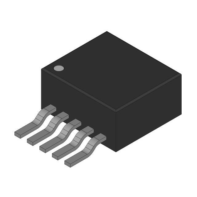
Device Information(1)
PART NUMBER PACKAGE
LM2587
BODY SIZE (NOM)
DDPAK/ TO-263 (5) 10.16 mm × 8.42 mm
TO-220 (5)
14.986 mm × 10.16 mm
(1) For all available packages, see the orderable addendum at
the end of the data sheet.
Flyback Regulator
1
An IMPORTANT NOTICE at the end of this data sheet addresses availability, warranty, changes, use in safety-critical applications,
intellectual property matters and other important disclaimers. PRODUCTION DATA.
�LM2587
SNVS115E – APRIL 2000 – REVISED JUNE 2019
www.ti.com
Table of Contents
1
2
3
4
5
6
Features ..................................................................
Typical Applications ..............................................
Description .............................................................
Revision History.....................................................
Pin Configurations.................................................
Specifications.........................................................
1
1
1
2
3
4
6.1
6.2
6.3
6.4
6.5
6.6
6.7
6.8
6.9
Absolute Maximum Ratings ..................................... 4
ESDRatings............................................................... 4
Recommended Operating Ratings............................ 4
Thermal Information .................................................. 5
Electrical Characteristics: 3.3 V ............................... 5
Electrical Characteristics: 5 V .................................. 6
Electrical Characteristics: 12 V ................................ 6
Electrical Characteristics: Adjustable ........................ 7
Electrical Characteristics: All Output Voltage Versions
...................................................................................7
6.10 Typical Characteristics ............................................ 9
7
Detailed Description ............................................ 12
7.1 Overview ................................................................. 12
7.2 Functional Block Diagram ....................................... 13
7.3 Feature Description................................................. 14
8
Application And Implementation........................ 15
8.1 Application Information............................................ 15
8.2 Typical Applications ................................................ 15
8.3 Additional Application Examples............................. 27
9
Layout ................................................................... 28
9.1 Layout Guidelines ................................................... 28
9.2 Layout Example ...................................................... 28
9.3 Heat Sink/Thermal Considerations ......................... 28
10 Device and Documentation Support ................. 31
10.1 Device Support......................................................
10.2 Receiving Notification Of Documentation
Updates....................................................................
10.3 Community Resources..........................................
10.4 Trademarks ...........................................................
10.5 Electrostatic Discharge Caution ............................
10.6 Glossary ................................................................
31
31
31
31
31
32
11 Mechanical, Packaging, and Orderable
Information ........................................................... 32
4 Revision History
NOTE: Page numbers for previous revisions may differ from page numbers in the current version.
Changes from Revision D (April 2013) to Revision E
•
Editorial changes only, no technical revisions; add links for WEBENCH .............................................................................. 1
Changes from Revision C (April 2013) to Revision D
•
2
Page
Page
Changed layout of National Data Sheet to TI format ........................................................................................................... 30
Submit Documentation Feedback
Copyright © 2000–2019, Texas Instruments Incorporated
Product Folder Links: LM2587
�LM2587
www.ti.com
SNVS115E – APRIL 2000 – REVISED JUNE 2019
5 Pin Configurations
NDH Package
5-Pin TO-220
Top View, Bent Staggered Leads
KTT Package
5-Pin DDPAK/TO-263
Top View
NDH Package
5-Pin TO-220
Side View, Bent Staggered Leads
KTT Package
5-Pin DDPAK/TO-263
Side View
Submit Documentation Feedback
Copyright © 2000–2019, Texas Instruments Incorporated
Product Folder Links: LM2587
3
�LM2587
SNVS115E – APRIL 2000 – REVISED JUNE 2019
www.ti.com
6 Specifications
6.1 Absolute Maximum Ratings
over operating free-air temperature range (unless otherwise noted) (1) (2)
−0.4V ≤ VIN ≤ 45V
Input Voltage
−0.4V ≤ VSW ≤ 65V
Switch Voltage
Switch Current (3)
Internally Limited
Compensation Pin Voltage
−0.4V ≤ VCOMP ≤ 2.4V
Feedback Pin Voltage
−0.4V ≤ VFB ≤ 2 VOUT
−65°C to +150°C
Storage Temperature Range
Lead Temperature
(Soldering, 10 sec.)
260°C
Maximum Junction
Temperature (4)
150°C
Power Dissipation
(1)
(2)
(3)
(4)
(4)
Internally Limited
Absolute Maximum Ratings indicate limits beyond which damage to the device may occur. Operating ratings indicate conditions the
device is intended to be functional, but device parameter specifications may not be specified under these conditions. For specifications
and test conditions see .
If Military/Aerospace specified devices are required, contact the Texas Instruments Sales Office/ Distributors for availability and
specifications.
Note that switch current and output current are not identical in a step-up regulator. Output current cannot be internally limited when the
LM2587 is used as a step-up regulator. To prevent damage to the switch, the output current must be externally limited to 5A. However,
output current is internally limited when the LM2587 is used as a flyback regulator (see the section for more information).
The junction temperature of the device (TJ) is a function of the ambient temperature (TA), the junction-to-ambient thermal resistance
(θJA), and the power dissipation of the device (PD). A thermal shutdown will occur if the temperature exceeds the maximum junction
temperature of the device: PD × θJA + TA(MAX) ≥ TJ(MAX). For a safe thermal design, check that the maximum power dissipated by the
device is less than: PD ≤ [TJ(MAX) − TA(MAX))]/θJA. When calculating the maximum allowable power dissipation, derate the maximum
junction temperature—this ensures a margin of safety in the thermal design.
6.2 ESDRatings
V(ESD)
(1)
Electrostatic discharge
(minimum)
Human-body model (HBM), per ANSI/ESDA/JEDEC JS-001 (1)
(C = 100 pF, R = 1.5 kΩ)
VALUE
UNIT
2000
V
JEDEC document JEP155 states that 500-V HBM allows safe manufacturing with a standard ESD control process.
6.3 Recommended Operating Ratings
4V ≤ VIN ≤ 40V
Supply Voltage
0V ≤ VSW ≤ 60V
Output Switch Voltage
ISW ≤ 5.0A
Output Switch Current
−40°C ≤ TJ ≤ +125°C
Junction Temperature Range
4
Submit Documentation Feedback
Copyright © 2000–2019, Texas Instruments Incorporated
Product Folder Links: LM2587
�LM2587
www.ti.com
SNVS115E – APRIL 2000 – REVISED JUNE 2019
6.4 Thermal Information
LM2585
THERMAL METRIC (1) (2)
RθJA
RθJC
(1)
(2)
(3)
(4)
(5)
(6)
(7)
KTT (DDPAK/TO-263
NDH (TO-220)
5 PINS
5 PINS
56 (3)
65 (4)
35
(5)
45 (6)
26
(7)
—
Junction-to-ambient thermal resistance
Junction-to-case thermal resistance
2
2
UNIT
°C/W
°C/W
For more information about traditional and new thermal metrics, see the Semiconductor and IC package thermal metrics application
report.
External components such as the diode, inductor, input and output capacitors can affect switching regulator performance. When the
LM2587 is used as shown in Figure 61 and Figure 62, system performance will be as specified by the system parameters.
Junction-to-ambient thermal resistance for the 5 lead TO-263 mounted horizontally against a PC board area of 0.136 square inches (the
same size as the TO-263 package) of 1 oz. (0.0014 in. thick) copper.
Junction-to-ambient thermal resistance (no external heat sink) for the 5 lead TO-220 package mounted vertically, with ½ inch leads in a
socket, or on a PC board with minimum copper area.
Junction-to-ambient thermal resistance for the 5 lead TO-263 mounted horizontally against a PC board area of 0.4896 square inches
(3.6 times the area of the TO-263 package) of 1 oz. (0.0014 in. thick) copper.
Junction-to-ambient thermal resistance (no external heat sink) for the 5 lead TO-220 package mounted vertically, with ½ inch leads
soldered to a PC board containing approximately 4 square inches of (1oz.) copper area surrounding the leads.
Junction-to-ambient thermal resistance for the 5 lead TO-263 mounted horizontally against a PC board copper area of 1.0064 square
inches (7.4 times the area of the TO-263 package) of 1 oz. (0.0014 in. thick) copper. Additional copper area reduces thermal resistance
further. See the thermal model in Switchers Made Simple® software.
6.5 Electrical Characteristics: 3.3 V
Specifications with standard type face are for TJ = 25°C, and those in bold apply over full Operating Temperature Range.
Unless otherwise specified, VIN = 5V.
PARAMETER
TEST CONDITIONS
SYSTEM PARAMETERS Test Circuit of Figure 61
TYP
MIN
MAX
UNIT
3.17/3.14
3.43/3.46
V
(1)
VOUT
Output Voltage
VIN = 4V to 12V
ILOAD = 400 mA to 1.75A
3.3
ΔVOUT/
ΔVIN
Line Regulation
VIN = 4V to 12V
ILOAD = 400 mA
20
50/100
mV
ΔVOUT/
ΔILOAD
Load Regulation
VIN = 12V
ILOAD = 400 mA to 1.75A
20
50/100
mV
η
Efficiency
VIN = 12V, ILOAD = 1A
75
UNIQUE DEVICE PARAMETERS
VREF
Output Reference
Voltage
Measured at Feedback Pin
VCOMP = 1.0V
3.3
ΔVREF
Reference Voltage
Line Regulation
VIN = 4V to 40V
2.0
GM
Error Amp
Transconductance
ICOMP = −30 μA to +30 μA
VCOMP = 1.0V
AVOL
Error Amp
Voltage Gain
VCOMP = 0.5V to 1.6V
RCOMP = 1.0 MΩ (3)
(1)
(2)
(3)
%
(2)
3.242/3.234
3.358/3.366
V
mV
1.193
0.678
260
151/75
2.259
mmho
V/V
External components such as the diode, inductor, input and output capacitors can affect switching regulator performance. When the
LM2587 is used as shown in Figure 61 and Figure 62, system performance will be as specified by the system parameters.
All room temperature limits are 100% production tested, and all limits at temperature extremes are specified via correlation using
standard Statistical Quality Control (SQC) methods.
A 1-MΩ resistor is connected to the compensation pin (which is the error amplifier output) to ensure accuracy in measuring AVOL.
Submit Documentation Feedback
Copyright © 2000–2019, Texas Instruments Incorporated
Product Folder Links: LM2587
5
�LM2587
SNVS115E – APRIL 2000 – REVISED JUNE 2019
www.ti.com
6.6 Electrical Characteristics: 5 V
Specifications with standard type face are for TJ = 25°C, and those in bold apply over full Operating Temperature Range.
Unless otherwise specified, VIN = 5V.
PARAMETER
TEST CONDITIONS
TYP
MIN
MAX
UNIT
4.80/4.75
5.20/5.25
V
SYSTEM PARAMETERS Test Circuit of Figure 61 (1)
VOUT
Output Voltage
VIN = 4V to 12V
ILOAD = 500 mA to 1.45A
5.0
ΔVOUT/
ΔVIN
Line Regulation
VIN = 4V to 12V
ILOAD = 500 mA
20
50/100
mV
ΔVOUT/
ΔILOAD
Load Regulation
VIN = 12V
ILOAD = 500 mA to 1.45A
20
50/100
mV
η
Efficiency
VIN = 12V, ILOAD = 750 mA
80
UNIQUE DEVICE PARAMETERS
VREF
Output Reference
Voltage
Measured at Feedback Pin
VCOMP = 1.0V
5.0
ΔVREF
Reference Voltage
Line Regulation
VIN = 4V to 40V
3.3
GM
Error Amp
Transconductance
ICOMP = −30 μA to +30 μA
VCOMP = 1.0V
AVOL
Error Amp
Voltage Gain
VCOMP = 0.5V to 1.6V
RCOMP = 1.0 MΩ (3)
(1)
(2)
(3)
%
(2)
4.913/4.900
5.088/5.100
V
mV
0.750
0.447
165
99/49
1.491
mmho
V/V
External components such as the diode, inductor, input and output capacitors can affect switching regulator performance. When the
LM2587 is used as shown in Figure 61 and Figure 62, system performance will be as specified by the system parameters.
All room temperature limits are 100% production tested, and all limits at temperature extremes are specified via correlation using
standard Statistical Quality Control (SQC) methods.
A 1-MΩ resistor is connected to the compensation pin (which is the error amplifier output) to ensure accuracy in measuring AVOL.
6.7 Electrical Characteristics: 12 V
Specifications with standard type face are for TJ = 25°C, and those in bold apply over full Operating Temperature Range.
Unless otherwise specified, VIN = 5V.
PARAMETER
TEST CONDITIONS
SYSTEM PARAMETERS Test Circuit of Figure 62
TYP
MIN
MAX
UNIT
12.0
11.52/11.40
12.48/12.60
V
(1)
VOUT
Output Voltage
VIN = 4V to 10V
ILOAD = 300 mA to 1.2A
ΔVOUT/
ΔVIN
Line Regulation
VIN = 4V to 10V
ILOAD = 300 mA
20
100/200
mV
ΔVOUT/
ΔILOAD
Load Regulation
VIN = 10V
ILOAD = 300 mA to 1.2A
20
100/200
mV
η
Efficiency
VIN = 10V, ILOAD = 1A
90
UNIQUE DEVICE PARAMETERS
VREF
Output Reference
Voltage
Measured at Feedback Pin
VCOMP = 1.0V
12.0
ΔVREF
Reference Voltage
Line Regulation
VIN = 4V to 40
7.8
GM
Error Amp
Transconductance
ICOMP = −30 μA to +30 μA
VCOMP = 1.0V
AVOL
Error Amp
Voltage Gain
VCOMP = 0.5V to 1.6V
RCOMP = 1.0 MΩ (3)
(1)
(2)
(3)
6
%
(2)
11.79/11.76
12.21/12.24
V
mV
0.328
0.186
70
41/21
0.621
mmho
V/V
External components such as the diode, inductor, input and output capacitors can affect switching regulator performance. When the
LM2587 is used as shown in Figure 61 and Figure 62, system performance will be as specified by the system parameters.
All room temperature limits are 100% production tested, and all limits at temperature extremes are specified via correlation using
standard Statistical Quality Control (SQC) methods.
A 1-MΩ resistor is connected to the compensation pin (which is the error amplifier output) to ensure accuracy in measuring AVOL.
Submit Documentation Feedback
Copyright © 2000–2019, Texas Instruments Incorporated
Product Folder Links: LM2587
�LM2587
www.ti.com
SNVS115E – APRIL 2000 – REVISED JUNE 2019
6.8 Electrical Characteristics: Adjustable
Specifications with standard type face are for TJ = 25°C, and those in bold type face apply over full Operating Temperature
Range. Unless otherwise specified, VIN = 5V.
PARAMETER
TEST CONDITIONS
TYP
MIN
MAX
UNIT
12.0
11.52/11.40
12.48/12.60
V
SYSTEM PARAMETERS Test Circuit of Figure 62 (1)
VOUT
Output Voltage
VIN = 4V to 10V
ILOAD = 300 mA to 1.2A
ΔVOUT/
ΔVIN
Line Regulation
VIN = 4V to 10V
ILOAD = 300 mA
20
100/200
mV
ΔVOUT/
ΔILOAD
Load Regulation
VIN = 10V
ILOAD = 300 mA to 1.2A
20
100/200
mV
η
Efficiency
VIN = 10V, ILOAD = 1A
90
UNIQUE DEVICE PARAMETERS
VREF
Output Reference
Voltage
Measured at Feedback Pin
VCOMP = 1.0V
ΔVREF
Reference Voltage
Line Regulation
VIN = 4V to 40V
GM
Error Amp
Transconductance
ICOMP = −30 μA to +30 μA
VCOMP = 1.0V
AVOL
Error Amp
Voltage Gain
IB
Error Amp
Input Bias Current
(1)
(2)
(3)
%
(2)
1.230
1.208/1.205
1.252/1.255
V
1.5
mV
3.200
1.800
VCOMP = 0.5V to 1.6V
RCOMP = 1.0 MΩ (3)
670
400/200
VCOMP = 1.0V
125
6.000
mmho
V/V
425/600
nA
External components such as the diode, inductor, input and output capacitors can affect switching regulator performance. When the
LM2587 is used as shown in Figure 61 and Figure 62, system performance will be as specified by the system parameters.
All room temperature limits are 100% production tested, and all limits at temperature extremes are specified via correlation using
standard Statistical Quality Control (SQC) methods.
A 1-MΩ resistor is connected to the compensation pin (which is the error amplifier output) to ensure accuracy in measuring AVOL.
6.9 Electrical Characteristics: All Output Voltage Versions
(1)
Specifications with standard type face are for TJ = 25°C, and those in bold type face apply over full Operating Temperature
Range. Unless otherwise specified, VIN = 5V.
PARAMETER
TEST CONDITIONS
MIN
Input Supply Current
ISWITCH = 3.0A
85
VUV
Input Supply
Undervoltage Lockout
RLOAD = 100Ω
3.30
3.05
fO
Oscillator Frequency
Measured at Switch Pin
RLOAD = 100Ω
VCOMP = 1.0V
100
85/75
Short-Circuit
Frequency
Measured at Switch Pin
RLOAD = 100Ω
VFEEDBACK = 1.15V
25
Error Amplifier
Output Swing
Upper Limit
See (3)
2.8
Lower Limit
See (2)
0.25
fSC
VEAO
IEAO
(1)
(2)
(3)
(4)
Error Amp
Output Current
(Source or Sink)
(Switch Off)
See (2)
TYP
IS
11
MAX
UNIT
15.5/16.5
mA
140/165
mA
3.75
V
115/125
kHz
kHz
2.6/2.4
V
0.40/0.55
V
260/320
μA
See (4)
165
110/70
All room temperature limits are 100% production tested, and all limits at temperature extremes are specified via correlation using
standard Statistical Quality Control (SQC) methods.
To measure this parameter, the feedback voltage is set to a high value, depending on the output version of the device, to force the error
amplifier output low. Adj: VFB = 1.41 V; 3.3 V: VFB = 3.8 V; 5 V: VFB = 5.75 V; 12 V: VFB = 13.8 V.
To measure this parameter, the feedback voltage is set to a low value, depending on the output version of the device, to force the error
amplifier output high. Adj: VFB = 1.05 V; 3.3 V: VFB = 2.81 V; 5 V: VFB = 4.25 V; 12 V: VFB = 10.2 V.
To measure the worst-case error amplifier output current, the LM2587 is tested with the feedback voltage set to its low value (specified
in Note 7) and at its high value (specified in Note 8).
Submit Documentation Feedback
Copyright © 2000–2019, Texas Instruments Incorporated
Product Folder Links: LM2587
7
�LM2587
SNVS115E – APRIL 2000 – REVISED JUNE 2019
www.ti.com
Electrical Characteristics: All Output Voltage Versions
(1)
(continued)
Specifications with standard type face are for TJ = 25°C, and those in bold type face apply over full Operating Temperature
Range. Unless otherwise specified, VIN = 5V.
PARAMETER
TEST CONDITIONS
TYP
MIN
MAX
UNIT
11.0
8.0/7.0
17.0/19.0
μA
RLOAD = 100Ω
See (3)
98
93/90
Switch Leakage
Current
Switch Off
VSWITCH = 60V
15
VSUS
Switch Sustaining
Voltage
dV/dT = 1.5V/ns
VSAT
Switch Saturation
Voltage
ISWITCH = 5.0A
ICL
NPN Switch
Current Limit
ISS
Soft Start Current
VFEEDBACK = 0.92V
VCOMP = 1.0V
D
Maximum Duty Cycle
IL
8
300/600
65
0.7
6.5
Submit Documentation Feedback
%
5.0
μA
V
1.1/1.4
V
9.5
A
Copyright © 2000–2019, Texas Instruments Incorporated
Product Folder Links: LM2587
�LM2587
www.ti.com
SNVS115E – APRIL 2000 – REVISED JUNE 2019
6.10 Typical Characteristics
Figure 1. Supply Current vs Temperature
Figure 2. Reference Voltage vs Temperature
Figure 3. ΔReference Voltage vs Supply Voltage
Figure 4. Supply Current vs Switch Current
Figure 5. Current Limit vs Temperature
Figure 6. Feedback Pin Bias Current vs Temperature
Submit Documentation Feedback
Copyright © 2000–2019, Texas Instruments Incorporated
Product Folder Links: LM2587
9
�LM2587
SNVS115E – APRIL 2000 – REVISED JUNE 2019
www.ti.com
Typical Characteristics (continued)
10
Figure 7. Switch Saturation Voltage vs Temperature
Figure 8. Switch Transconductance vs Temperature
Figure 9. Oscillator Frequency vs Temperature
Figure 10. Error Amp Transconductance vs Temperature
Figure 11. Error Amp Voltage Gain vs Temperature
Figure 12. Short Circuit Frequency vs Temperature
Submit Documentation Feedback
Copyright © 2000–2019, Texas Instruments Incorporated
Product Folder Links: LM2587
�LM2587
www.ti.com
SNVS115E – APRIL 2000 – REVISED JUNE 2019
Typical Characteristics (continued)
A: Switch Voltage, 10 V/div B: Switch Current, 5 A/div C: Output
Rectifier Current, 5 A/div D: Output Ripple Voltage, 100 mV/div
AC-Coupled
Horizontal: 2 μs/div
Figure 13. Switching Waveforms
Figure 14. VOUT Load Current Step Response
Submit Documentation Feedback
Copyright © 2000–2019, Texas Instruments Incorporated
Product Folder Links: LM2587
11
�LM2587
SNVS115E – APRIL 2000 – REVISED JUNE 2019
www.ti.com
7 Detailed Description
7.1 Overview
The LM2587 is ideally suited for use in the flyback regulator topology. The flyback regulator can produce a single
output voltage, such as the one shown in Figure 15, or multiple output voltages. In Figure 15, the flyback
regulator generates an output voltage that is inside the range of the input voltage. This feature is unique to
flyback regulators and cannot be duplicated with buck or boost regulators.
The operation of a flyback regulator is as follows (refer to Figure 15): when the switch is on, current flows
through the primary winding of the transformer, T1, storing energy in the magnetic field of the transformer. Note
that the primary and secondary windings are out of phase, so no current flows through the secondary when
current flows through the primary. When the switch turns off, the magnetic field collapses, reversing the voltage
polarity of the primary and secondary windings. Now rectifier D1 is forward biased and current flows through it,
releasing the energy stored in the transformer. This produces voltage at the output.
The output voltage is controlled by modulating the peak switch current. This is done by feeding back a portion of
the output voltage to the error amp, which amplifies the difference between the feedback voltage and a 1.23-V
reference. The error amp output voltage is compared to a ramp voltage proportional to the switch current (in
other words, inductor current during the switch on time). The comparator terminates the switch on time when the
two voltages are equal, thereby controlling the peak switch current to maintain a constant output voltage.
As shown in Figure 15, the LM2587 can be used as a flyback regulator by using a minimum number of external
components. The switching waveforms of this regulator are shown in Figure 13. Typical Performance
Characteristics observed during the operation of this circuit are shown in Figure 14.
Figure 15. 12-V Flyback Regulator Design Example
12
Submit Documentation Feedback
Copyright © 2000–2019, Texas Instruments Incorporated
Product Folder Links: LM2587
�LM2587
www.ti.com
SNVS115E – APRIL 2000 – REVISED JUNE 2019
7.2 Functional Block Diagram
For Fixed Versions 3.3 V, R1 = 3.4 k, R2 = 2 k, 5 V, R1 = 6.15 k, R2 = 2k 12V, R1 = 8.73 k, R2 = 1 k. For Adj. Version R1 =
Short (0Ω), R2 = Open
Submit Documentation Feedback
Copyright © 2000–2019, Texas Instruments Incorporated
Product Folder Links: LM2587
13
�LM2587
SNVS115E – APRIL 2000 – REVISED JUNE 2019
www.ti.com
For Fixed Versions 3.3 V, R1 = 3.4 k, R2 = 2 k, 5 V, R1 = 6.15 k, R2 = 2k 12V, R1 = 8.73 k, R2 = 1 k. For Adj. Version R1 =
Short (0Ω), R2 = Open
7.3 Feature Description
7.3.1 Step-Up (Boost) Regulator Operation
Figure 16 shows the LM2587 used as a step-up (boost) regulator. This is a switching regulator that produces an
output voltage greater than the input supply voltage.
A brief explanation of how the LM2587 Boost Regulator works is as follows (refer to Figure 16). When the NPN
switch turns on, the inductor current ramps up at the rate of VIN/L, storing energy in the inductor. When the
switch turns off, the lower end of the inductor flies above VIN, discharging its current through diode (D) into the
output capacitor (COUT) at a rate of (VOUT − VIN)/L. Thus, energy stored in the inductor during the switch on time
is transferred to the output during the switch off time. The output voltage is controlled by adjusting the peak
switch current, as described in the section.
By adding a small number of external components (as shown in Figure 16), the LM2587 can be used to produce a
regulated output voltage that is greater than the applied input voltage. The switching waveforms observed during the
operation of this circuit are shown in . Typical performance of this regulator is shown in .
Figure 16. 12-V Boost Regulator
14
Submit Documentation Feedback
Copyright © 2000–2019, Texas Instruments Incorporated
Product Folder Links: LM2587
�LM2587
www.ti.com
SNVS115E – APRIL 2000 – REVISED JUNE 2019
8 Application And Implementation
8.1 Application Information
The LM2587 series of regulators are monolithic integrated circuits specifically designed for flyback, step-up
(boost), and forward converter applications. Requiring a minimum number of external components, these
regulators are cost effective and simple to use.
8.2 Typical Applications
8.2.1 Typical Boost Regulator Applications
Figure 18 through Figure 21 show four typical boost applications)—one fixed and three using the adjustable
version of the LM2587. Each drawing contains the part number(s) and manufacturer(s) for every component. For
the fixed 12-V output application, the part numbers and manufacturers' names for the inductor are listed in . For
applications with different output voltages, refer to the Switchers Made Simple software.
Figure 17. Boost Regulator
Figure 18. 5-V To 12-V Boost Regulator
Figure 19. 12-V To 24-V Boost Regulator
Submit Documentation Feedback
Copyright © 2000–2019, Texas Instruments Incorporated
Product Folder Links: LM2587
15
�LM2587
SNVS115E – APRIL 2000 – REVISED JUNE 2019
www.ti.com
Typical Applications (continued)
Figure 20. 24-V To 36-V Boost Regulator
*The LM2585 will require a heat sink in these applications. The size of the heat sink will depend on the maximum
ambient temperature. To calculate the thermal resistance of the IC and the size of the heat sink needed, see
Figure 21. 24-V To 48-V Boost Regulator
8.2.2 Typical Flyback Regulator Applications
Figure 24 Figure 25 Figure 26 show six typical flyback applications, varying from single output to triple output.
Each drawing contains the part number(s) and manufacturer(s) for every component except the transformer. For
the transformer part numbers and manufacturers names, see the table in . For applications with different output
voltages—requiring the LM2587-ADJ—or different output configurations that do not match the standard
configurations, refer to the Switchers Made Simple software.
16
Submit Documentation Feedback
Copyright © 2000–2019, Texas Instruments Incorporated
Product Folder Links: LM2587
�LM2587
www.ti.com
SNVS115E – APRIL 2000 – REVISED JUNE 2019
Typical Applications (continued)
Figure 22. Single-Output Flyback Regulator
Figure 23. Single-Output Flyback Regulator
Submit Documentation Feedback
Copyright © 2000–2019, Texas Instruments Incorporated
Product Folder Links: LM2587
17
�LM2587
SNVS115E – APRIL 2000 – REVISED JUNE 2019
www.ti.com
Typical Applications (continued)
Figure 24. Single-Output Flyback Regulator
Figure 25. Dual-Output Flyback Regulator
18
Submit Documentation Feedback
Copyright © 2000–2019, Texas Instruments Incorporated
Product Folder Links: LM2587
�LM2587
www.ti.com
SNVS115E – APRIL 2000 – REVISED JUNE 2019
Typical Applications (continued)
Figure 26. Dual-Output Flyback Regulator
Figure 27. Triple-Output Flyback Regulator
Submit Documentation Feedback
Copyright © 2000–2019, Texas Instruments Incorporated
Product Folder Links: LM2587
19
�LM2587
SNVS115E – APRIL 2000 – REVISED JUNE 2019
www.ti.com
Typical Applications (continued)
8.2.2.1 Transformer Selection (T)
lists the standard transformers available for flyback regulator applications. Included in the table are the turns
ratio(s) for each transformer, as well as the output voltages, input voltage ranges, and the maximum load
currents for each circuit.
Table 1. Transformer Selection Table
Applications
Transformers
VIN
Figure 24
Figure 25
Figure 26
T1
T1
T1
T2
T3
Figure 27
T4
4V–6V
4V–6V
8V–16V
4V–6V
18V–36V
18V–36V
VOUT1
3.3V
5V
12V
12V
12V
5V
IOUT1 (Max)
1.8A
1.4A
1.2A
0.3A
1A
2.5A
1
1
1
2.5
0.8
0.35
VOUT2
−12V
−12V
12V
IOUT2 (Max)
0.3A
1A
0.5A
2.5
0.8
0.8
N1
N2
VOUT3
−12V
IOUT3 (Max)
0.5A
N3
0.8
Table 2. Transformer Manufacturer Guide
Manufacturers' Part Numbers
Transform
er Type
(1)
(2)
(3)
(4)
Coilcraft
Pulse
Surface Mount
Surface Mount
Coilcraft
(1)
(1)
(2)
Pulse
Renco
Schott
(2)
(3)
(4)
T5
Q4338-B
Q4437-B
PE-68413
—
RL-5532
67140890
T6
Q4339-B
Q4438-B
PE-68414
—
RL-5533
67140900
T7
S6000-A
S6057-A
—
PE-68482
RL-5751
26606
Coilcraft Inc. Phone: (800) 322-2645 www.coilcraft.com
Pulse Engineering Inc. Phone: (619) 674-8100 www.digikey.com
Renco Electronics Inc. Phone: (800) 645-5828 www.cdiweb.com/renco
Schott Corp. Phone: (612) 475-1173 www.schottcorp.com/
8.2.2.2 Transformer Footprints
through Figure 58 show the footprints of each transformer, listed in .
Figure 28. Coilcraft Q4434-B (Top View)
Figure 29. Coilcraft Q4337-B (Top View)
Figure 30. Coilcraft Q4343-B (Top View)
Figure 31. Coilcraft Q4344-B (Top View)
20
Submit Documentation Feedback
Copyright © 2000–2019, Texas Instruments Incorporated
Product Folder Links: LM2587
�LM2587
www.ti.com
SNVS115E – APRIL 2000 – REVISED JUNE 2019
Figure 32. Coilcraft Q4435-B (Surface Mount) (Top View)
Figure 33. Coilcraft Q4436-B (Surface Mount) (Top View)
Figure 34. Pulse PE-68411 (Surface Mount) (Top View)
Figure 35. Pulse PE-68412 (Surface Mount) (Top View)
Figure 36. Pulse PE-68421 (Surface Mount) (Top View)
Figure 37. Pulse PE-68422 (Surface Mount) (Top View)
Figure 38. Renco RL-5530 (Top View)
Figure 39. Renco RL-5531 (Top View)
Figure 40. Renco RL-5534 (Top View)
Figure 41. Renco RL-5535 (Top View)
Figure 42. Schott 67141450 (Top View)
Figure 43. Schott 67140860 (Top View)
Figure 44. Schott 67140920 (Top View)
Figure 45. Schott 67140930 (Top View)
Submit Documentation Feedback
Copyright © 2000–2019, Texas Instruments Incorporated
Product Folder Links: LM2587
21
�LM2587
SNVS115E – APRIL 2000 – REVISED JUNE 2019
22
www.ti.com
Figure 46. Coilcraft Q4437-B (Top View)
(Surface Mount)
Figure 47. Coilcraft Q4338-B
(Top View)
Figure 48. Coilcraft S6057-A (Top View)
(Surface Mount)
Figure 49. Coilcraft Q4438-B (Top View)
(Surface Mount)
Figure 50. Pulse Pe-68482 (Top View)
Figure 51. Pulse Pe-68414 (Top View)
(Surface Mount)
Figure 52. Pulse Pe-68413 (Top View)
(Surface Mount)
Figure 53. Renco Rl-5751 (Top View)
Submit Documentation Feedback
Copyright © 2000–2019, Texas Instruments Incorporated
Product Folder Links: LM2587
�LM2587
www.ti.com
SNVS115E – APRIL 2000 – REVISED JUNE 2019
Figure 54. Renco Rl-5533
(Top View)
Figure 55. Renco Rl-5532 (Top View)
Figure 56. Schott 26606 (Top View)
Figure 57. Schott 67140900 (Top View)
Figure 58. Schott 67140890
(Top View)
Submit Documentation Feedback
Copyright © 2000–2019, Texas Instruments Incorporated
Product Folder Links: LM2587
23
�LM2587
SNVS115E – APRIL 2000 – REVISED JUNE 2019
www.ti.com
8.2.3 Design Requirements
Table 3 contains a table of standard inductors, by part number and corresponding manufacturer, for the fixed
output regulator of Figure 18.
Table 3. Inductor Selection Table
Coilcraft
(1)
Pulse
R4793-A
(1)
(2)
(3)
(4)
(2)
PE-53900
Renco (3)
Schott (4)
RL-5472-5
67146520
Coilcraft Inc.,: Phone: (800) 322-26451102 Silver Lake Road, Cary, IL 60013: Fax: (708) 639-1469
Pulse Engineering Inc.,: Phone: (619) 674-810012220 World Trade Drive, San Diego, CA 92128: Fax: (619) 674-8262
Renco Electronics Inc.,: Phone: (800) 645-582860 Jeffryn Blvd. East, Deer Park, NY 11729: Fax: (516) 586-5562
Schott Corp.,: Phone: (612) 475-11731000 Parkers Lane Road, Wayzata, MN 55391: Fax: (612) 475-1786
8.2.4 Detailed Design Procedure
8.2.4.1 Custom Design With Webench® Tools
Click here to create a custom design using the LM2587 device with the WEBENCH® Power Designer.
1. Start by entering the input voltage (VIN), output voltage (VOUT), and output current (IOUT) requirements.
2. Optimize the design for key parameters such as efficiency, footprint, and cost using the optimizer dial.
3. Compare the generated design with other possible solutions from Texas Instruments.
The WEBENCH Power Designer provides a customized schematic along with a list of materials with real-time
pricing and component availability.
In most cases, these actions are available:
• Run electrical simulations to see important waveforms and circuit performance
• Run thermal simulations to understand board thermal performance
• Export customized schematic and layout into popular CAD formats
• Print PDF reports for the design, and share the design with colleagues
Get more information about WEBENCH tools at www.ti.com/WEBENCH.
8.2.4.2 Programming Output Voltage (Selecting R1 And R2)
Referring to the adjustable regulator in Figure 17, the output voltage is programmed by the resistors R1 and R2
by the following formula:
VOUT = VREF (1 + R1/R2)
where VREF = 1.23V
(1)
Resistors R1 and R2 divide the output voltage down so that it can be compared with the 1.23V internal reference.
With R2 between 1k and 5k, R1 is:
R1 = R2 (VOUT/VREF − 1)
where VREF = 1.23V
(2)
For best temperature coefficient and stability with time, use 1% metal film resistors.
8.2.4.3 Short Circuit Condition
Due to the inherent nature of boost regulators, when the output is shorted (see Figure 17), current flows directly
from the input, through the inductor and the diode, to the output, bypassing the switch. The current limit of the
switch does not limit the output current for the entire circuit. To protect the load and prevent damage to the
switch, the current must be externally limited, either by the input supply or at the output with an external current
limit circuit. The external limit should be set to the maximum switch current of the device, which is 5A.
In a flyback regulator application (Figure 59), using the standard transformers, the LM2587 will survive a short
circuit to the main output. When the output voltage drops to 80% of its nominal value, the frequency will drop to
25 kHz. With a lower frequency, off times are larger. With the longer off times, the transformer can release all of
its stored energy before the switch turns back on. Hence, the switch turns on initially with zero current at its
collector. In this condition, the switch current limit will limit the peak current, saving the device.
24
Submit Documentation Feedback
Copyright © 2000–2019, Texas Instruments Incorporated
Product Folder Links: LM2587
�LM2587
www.ti.com
SNVS115E – APRIL 2000 – REVISED JUNE 2019
8.2.4.4 Flyback Regulator Input Capacitors
A flyback regulator draws discontinuous pulses of current from the input supply. Therefore, there are two input
capacitors needed in a flyback regulator; one for energy storage and one for filtering (see Figure 59). Both are
required due to the inherent operation of a flyback regulator. To keep a stable or constant voltage supply to the
LM2587, a storage capacitor (≥100 μF) is required. If the input source is a recitified DC supply and/or the
application has a wide temperature range, the required rms current rating of the capacitor might be very large.
This means a larger value of capacitance or a higher voltage rating will be needed of the input capacitor. The
storage capacitor will also attenuate noise which may interfere with other circuits connected to the same input
supply voltage.
Figure 59. Flyback Regulator
In addition, a small bypass capacitor is required due to the noise generated by the input current pulses. To
eliminate the noise, insert a 1.0 μF ceramic capacitor between VIN and ground as close as possible to the device.
8.2.4.5 Switch Voltage Limits
In a flyback regulator, the maximum steady-state voltage appearing at the switch, when it is off, is set by the
transformer turns ratio, N, the output voltage, VOUT, and the maximum input voltage, VIN (Max):
VSW(OFF) = VIN (Max) + (VOUT +VF)/N
(3)
where VF is the forward biased voltage of the output diode, and is 0.5V for Schottky diodes and 0.8V for ultra-fast
recovery diodes (typically). In certain circuits, there exists a voltage spike, VLL, superimposed on top of the
steady-state voltage (see Figure 13, waveform A). Usually, this voltage spike is caused by the transformer
leakage inductance and/or the output rectifier recovery time. To “clamp” the voltage at the switch from exceeding
its maximum value, a transient suppressor in series with a diode is inserted across the transformer primary (as
shown in the circuit on the front page and other flyback regulator circuits throughout the datasheet). The
schematic in Figure 59 shows another method of clamping the switch voltage. A single voltage transient
suppressor (the SA51A) is inserted at the switch pin. This method clamps the total voltage across the switch, not
just the voltage across the primary.
If poor circuit layout techniques are used (see the Layout Guidelines section), negative voltage transients may
appear on the Switch pin (pin 4). Applying a negative voltage (with respect to the IC's ground) to any monolithic
IC pin causes erratic and unpredictable operation of that IC. This holds true for the LM2587 IC as well. When
used in a flyback regulator, the voltage at the Switch pin (pin 4) can go negative when the switch turns on. The
“ringing” voltage at the switch pin is caused by the output diode capacitance and the transformer leakage
inductance forming a resonant circuit at the secondary(ies). The resonant circuit generates the “ringing” voltage,
which gets reflected back through the transformer to the switch pin. There are two common methods to avoid this
problem. One is to add an RC snubber around the output rectifier(s), as in Figure 59. The values of the resistor
and the capacitor must be chosen so that the voltage at the Switch pin does not drop below −0.4V. The resistor
may range in value between 10Ω and 1 kΩ, and the capacitor will vary from 0.001 μF to 0.1 μF. Adding a
snubber will (slightly) reduce the efficiency of the overall circuit.
Submit Documentation Feedback
Copyright © 2000–2019, Texas Instruments Incorporated
Product Folder Links: LM2587
25
�LM2587
SNVS115E – APRIL 2000 – REVISED JUNE 2019
www.ti.com
The other method to reduce or eliminate the “ringing” is to insert a Schottky diode clamp between pins 4 and 3
(ground), also shown in Figure 59. This prevents the voltage at pin 4 from dropping below −0.4V. The reverse
voltage rating of the diode must be greater than the switch off voltage.
Figure 60. Input Line Filter
8.2.4.6 Output Voltage Limitations
The maximum output voltage of a boost regulator is the maximum switch voltage minus a diode drop. In a
flyback regulator, the maximum output voltage is determined by the turns ratio, N, and the duty cycle, D, by the
equation:
VOUT ≈ N × VIN × D/(1 − D)
(4)
The duty cycle of a flyback regulator is determined by the following equation:
(5)
Theoretically, the maximum output voltage can be as large as desired—just keep increasing the turns ratio of the
transformer. However, there exists some physical limitations that prevent the turns ratio, and thus the output
voltage, from increasing to infinity. The physical limitations are capacitances and inductances in the LM2587
switch, the output diode(s), and the transformer—such as reverse recovery time of the output diode (mentioned
above).
8.2.4.7 Noisy Input Line Condition)
A small, low-pass RC filter should be used at the input pin of the LM2587 if the input voltage has an unusual
large amount of transient noise, such as with an input switch that bounces. The circuit in Figure 60 demonstrates
the layout of the filter, with the capacitor placed from the input pin to ground and the resistor placed between the
input supply and the input pin. Note that the values of RIN and CIN shown in the schematic are good enough for
most applications, but some readjusting might be required for a particular application. If efficiency is a major
concern, replace the resistor with a small inductor (say 10 μH and rated at 100 mA).
8.2.4.8 Stability
All current-mode controlled regulators can suffer from an instability, known as subharmonic oscillation, if they
operate with a duty cycle above 50%. To eliminate subharmonic oscillations, a minimum value of inductance is
required to ensure stability for all boost and flyback regulators. The minimum inductance is given by:
where
•
26
VSAT is the switch saturation voltage and can be found in the Characteristic Curves.
Submit Documentation Feedback
(6)
Copyright © 2000–2019, Texas Instruments Incorporated
Product Folder Links: LM2587
�LM2587
www.ti.com
SNVS115E – APRIL 2000 – REVISED JUNE 2019
8.3 Additional Application Examples
8.3.1 Test Circuits
CIN1—100 μF, 25V Aluminum Electrolytic CIN2—0.1 μF CeramicT—22 μH, 1:1 Schott
#67141450D—1N5820COUT—680 μF, 16V Aluminum Electrolytic CC—0.47 μF Ceramic RC—2k
Figure 61. LM2587-3.3 and LM2587-5.0 Test Circuit
CIN1—100 μF, 25V Aluminum Electrolytic CIN2—0.1 μF CeramicL—15 μH, Renco #RL-5472-5D—1N5820COUT—680
μF, 16V Aluminum Electrolytic CC—0.47 μF Ceramic RC—2kFor 12V Devices: R1 = Short (0Ω) and R2 = Open For
ADJ Devices: R1 = 48.75k, ±0.1% and R2 = 5.62k, ±1%
Figure 62. LM2587-12 and LM2587-ADJ Test Circuit
Submit Documentation Feedback
Copyright © 2000–2019, Texas Instruments Incorporated
Product Folder Links: LM2587
27
�LM2587
SNVS115E – APRIL 2000 – REVISED JUNE 2019
www.ti.com
9 Layout
9.1 Layout Guidelines
As in any switching regulator, layout is very important. Rapidly switching currents associated with wiring
inductance generate voltage transients which can cause problems. For minimal inductance and ground loops,
keep the length of the leads and traces as short as possible. Use single point grounding or ground plane
construction for best results. Separate the signal grounds from the power grounds (as indicated in Figure 63).
When using the adjustable version, physically locate the programming resistors as near the regulator IC as
possible, to keep the sensitive feedback wiring short.
9.2 Layout Example
Figure 63. Circuit Board Layout
9.3 Heat Sink/Thermal Considerations
In many cases, no heat sink is required to keep the LM2587 junction temperature within the allowed operating
range. For each application, to determine whether or not a heat sink will be required, the following must be
identified:
1) Maximum ambient temperature (in the application).
2) Maximum regulator power dissipation (in the application).
3) Maximum allowed junction temperature (125°C for the LM2587). For a safe, conservative design, a
temperature approximately 15°C cooler than the maximum junction temperature should be selected (110°C).
4) LM2587 package thermal resistances θJA and θJC (given in the Electrical Characteristics).
Total power dissipated (PD) by the LM2587 can be estimated as follows:
28
Submit Documentation Feedback
Copyright © 2000–2019, Texas Instruments Incorporated
Product Folder Links: LM2587
�LM2587
www.ti.com
SNVS115E – APRIL 2000 – REVISED JUNE 2019
Heat Sink/Thermal Considerations (continued)
Boost:
(7)
VIN is the minimum input voltage, VOUT is the output voltage, N is the transformer turns ratio, D is the duty cycle,
and ILOAD is the maximum load current (and ∑ILOAD is the sum of the maximum load currents for multiple-output
flyback regulators). The duty cycle is given by:
Boost:
where
•
•
VF is the forward biased voltage of the diode and is typically 0.5V for Schottky diodes and 0.8V for fast
recovery diodes.
VSAT is the switch saturation voltage and can be found in the Characteristic Curves.
(8)
When no heat sink is used, the junction temperature rise is:
ΔTJ = PD × θJA.
(9)
Adding the junction temperature rise to the maximum ambient temperature gives the actual operating junction
temperature:
TJ = ΔTJ + TA.
(10)
If the operating junction temperature exceeds the maximum junction temperatue in item 3 above, then a heat
sink is required. When using a heat sink, the junction temperature rise can be determined by the following:
ΔTJ = PD × (θJC + θInterface + θHeat Sink)
(11)
Again, the operating junction temperature will be:
TJ = ΔTJ + TA
(12)
As before, if the maximum junction temperature is exceeded, a larger heat sink is required (one that has a lower
thermal resistance).
Included in the Switchers Made Simple design software is a more precise (non-linear) thermal model that can
be used to determine junction temperature with different input-output parameters or different component values.
It can also calculate the heat sink thermal resistance required to maintain the regulator junction temperature
below the maximum operating temperature.
To further simplify the flyback regulator design procedure, TI is making available computer design software.
Switchers Made Simple software is available on a (3½″) diskette for IBM compatible computers from a TI sales
office in your area or the TI WEBENCH Design Center team.
http://www.ti.com/ww/en/analog/webench/index.shtml?DCMP=hpa_sva_webench&HQS=webench-bb
Submit Documentation Feedback
Copyright © 2000–2019, Texas Instruments Incorporated
Product Folder Links: LM2587
29
�LM2587
SNVS115E – APRIL 2000 – REVISED JUNE 2019
www.ti.com
Heat Sink/Thermal Considerations (continued)
9.3.1 European Magnetic Vendor
Contacts
Please contact the following addresses for details of local distributors or representatives:
9.3.2 Coilcraft
21 Napier Place
Wardpark North Cumbernauld, Scotland G68 0LL Phone: +44 1236 730 595 Fax: +44 1236 730 627
9.3.3 Pulse Engineering
Dunmore Road
Tuam Co. Galway, Ireland Phone: +353 93 24 107 Fax: +353 93 24 459
30
Submit Documentation Feedback
Copyright © 2000–2019, Texas Instruments Incorporated
Product Folder Links: LM2587
�LM2587
www.ti.com
SNVS115E – APRIL 2000 – REVISED JUNE 2019
10 Device and Documentation Support
10.1 Device Support
10.1.1 Third-Party Products Disclaimer
TI'S PUBLICATION OF INFORMATION REGARDING THIRD-PARTY PRODUCTS OR SERVICES DOES NOT
CONSTITUTE AN ENDORSEMENT REGARDING THE SUITABILITY OF SUCH PRODUCTS OR SERVICES
OR A WARRANTY, REPRESENTATION OR ENDORSEMENT OF SUCH PRODUCTS OR SERVICES, EITHER
ALONE OR IN COMBINATION WITH ANY TI PRODUCT OR SERVICE.
10.1.2 Development Support
10.1.2.1 Custom Design With Webench® Tools
Click here to create a custom design using the LM2587 device with the WEBENCH® Power Designer.
1. Start by entering the input voltage (VIN), output voltage (VOUT), and output current (IOUT) requirements.
2. Optimize the design for key parameters such as efficiency, footprint, and cost using the optimizer dial.
3. Compare the generated design with other possible solutions from Texas Instruments.
The WEBENCH Power Designer provides a customized schematic along with a list of materials with real-time
pricing and component availability.
In most cases, these actions are available:
• Run electrical simulations to see important waveforms and circuit performance
• Run thermal simulations to understand board thermal performance
• Export customized schematic and layout into popular CAD formats
• Print PDF reports for the design, and share the design with colleagues
Get more information about WEBENCH tools at www.ti.com/WEBENCH.
10.2 Receiving Notification Of Documentation Updates
To receive notification of documentation updates, navigate to the device product folder on ti.com. In the upper
right corner, click on Alert me to register and receive a weekly digest of any product information that has
changed. For change details, review the revision history included in any revised document.
10.3 Community Resources
The following links connect to TI community resources. Linked contents are provided "AS IS" by the respective
contributors. They do not constitute TI specifications and do not necessarily reflect TI's views; see TI's Terms of
Use.
TI E2E™ Online Community TI's Engineer-to-Engineer (E2E) Community. Created to foster collaboration
among engineers. At e2e.ti.com, you can ask questions, share knowledge, explore ideas and help
solve problems with fellow engineers.
Design Support TI's Design Support Quickly find helpful E2E forums along with design support tools and
contact information for technical support.
10.4 Trademarks
E2E is a trademark of Texas Instruments.
WEBENCH, Switchers Made Simple are registered trademarks of Texas Instruments.
All other trademarks are the property of their respective owners.
10.5 Electrostatic Discharge Caution
This integrated circuit can be damaged by ESD. Texas Instruments recommends that all integrated circuits be handled with
appropriate precautions. Failure to observe proper handling and installation procedures can cause damage.
ESD damage can range from subtle performance degradation to complete device failure. Precision integrated circuits may be more
susceptible to damage because very small parametric changes could cause the device not to meet its published specifications.
Submit Documentation Feedback
Copyright © 2000–2019, Texas Instruments Incorporated
Product Folder Links: LM2587
31
�LM2587
SNVS115E – APRIL 2000 – REVISED JUNE 2019
www.ti.com
10.6 Glossary
SLYZ022 — TI Glossary.
This glossary lists and explains terms, acronyms, and definitions.
11 Mechanical, Packaging, and Orderable Information
The following pages include mechanical, packaging, and orderable information. This information is the most
current data available for the designated devices. This data is subject to change without notice and revision of
this document. For browser-based versions of this data sheet, refer to the left-hand navigation.
32
Submit Documentation Feedback
Copyright © 2000–2019, Texas Instruments Incorporated
Product Folder Links: LM2587
�PACKAGE OPTION ADDENDUM
www.ti.com
30-Sep-2021
PACKAGING INFORMATION
Orderable Device
Status
(1)
Package Type Package Pins Package
Drawing
Qty
Eco Plan
(2)
Lead finish/
Ball material
MSL Peak Temp
Op Temp (°C)
Device Marking
(3)
(4/5)
(6)
LM2587S-12/NOPB
ACTIVE
DDPAK/
TO-263
KTT
5
45
RoHS-Exempt
& Green
SN
Level-3-245C-168 HR
-40 to 125
LM2587S
-12 P+
LM2587S-3.3/NOPB
ACTIVE
DDPAK/
TO-263
KTT
5
45
RoHS-Exempt
& Green
SN
Level-3-245C-168 HR
-40 to 125
LM2587S
-3.3 P+
LM2587S-5.0
NRND
DDPAK/
TO-263
KTT
5
45
Non-RoHS
& Green
Call TI
Level-3-235C-168 HR
-40 to 125
LM2587S
-5.0 P+
LM2587S-5.0/NOPB
ACTIVE
DDPAK/
TO-263
KTT
5
45
RoHS-Exempt
& Green
SN
Level-3-245C-168 HR
-40 to 125
LM2587S
-5.0 P+
LM2587S-ADJ
NRND
DDPAK/
TO-263
KTT
5
45
Non-RoHS
& Green
Call TI
Level-3-235C-168 HR
-40 to 125
LM2587S
-ADJ P+
LM2587S-ADJ/NOPB
ACTIVE
DDPAK/
TO-263
KTT
5
45
RoHS-Exempt
& Green
SN
Level-3-245C-168 HR
-40 to 125
LM2587S
-ADJ P+
LM2587SX-12/NOPB
ACTIVE
DDPAK/
TO-263
KTT
5
500
RoHS-Exempt
& Green
SN
Level-3-245C-168 HR
-40 to 125
LM2587S
-12 P+
LM2587SX-5.0/NOPB
ACTIVE
DDPAK/
TO-263
KTT
5
500
RoHS-Exempt
& Green
SN
Level-3-245C-168 HR
-40 to 125
LM2587S
-5.0 P+
LM2587SX-ADJ
NRND
DDPAK/
TO-263
KTT
5
500
Non-RoHS
& Green
Call TI
Level-3-235C-168 HR
-40 to 125
LM2587S
-ADJ P+
LM2587SX-ADJ/NOPB
ACTIVE
DDPAK/
TO-263
KTT
5
500
RoHS-Exempt
& Green
SN
Level-3-245C-168 HR
-40 to 125
LM2587S
-ADJ P+
LM2587T-12/NOPB
ACTIVE
TO-220
NDH
5
45
RoHS-Exempt
& Green
SN
Level-1-NA-UNLIM
-40 to 125
LM2587T
-12 P+
LM2587T-3.3/NOPB
ACTIVE
TO-220
NDH
5
45
RoHS-Exempt
& Green
SN
Level-1-NA-UNLIM
-40 to 125
LM2587T
-3.3 P+
LM2587T-5.0/NOPB
ACTIVE
TO-220
NDH
5
45
RoHS-Exempt
& Green
SN
Level-1-NA-UNLIM
-40 to 125
LM2587T
-5.0 P+
LM2587T-ADJ
NRND
TO-220
NDH
5
45
Non-RoHS
& Green
Call TI
Level-1-NA-UNLIM
-40 to 125
LM2587T
-ADJ P+
LM2587T-ADJ/NOPB
ACTIVE
TO-220
NDH
5
45
RoHS-Exempt
& Green
SN
Level-1-NA-UNLIM
-40 to 125
LM2587T
-ADJ P+
(1)
The marketing status values are defined as follows:
ACTIVE: Product device recommended for new designs.
LIFEBUY: TI has announced that the device will be discontinued, and a lifetime-buy period is in effect.
Addendum-Page 1
Samples
�PACKAGE OPTION ADDENDUM
www.ti.com
30-Sep-2021
NRND: Not recommended for new designs. Device is in production to support existing customers, but TI does not recommend using this part in a new design.
PREVIEW: Device has been announced but is not in production. Samples may or may not be available.
OBSOLETE: TI has discontinued the production of the device.
(2)
RoHS: TI defines "RoHS" to mean semiconductor products that are compliant with the current EU RoHS requirements for all 10 RoHS substances, including the requirement that RoHS substance
do not exceed 0.1% by weight in homogeneous materials. Where designed to be soldered at high temperatures, "RoHS" products are suitable for use in specified lead-free processes. TI may
reference these types of products as "Pb-Free".
RoHS Exempt: TI defines "RoHS Exempt" to mean products that contain lead but are compliant with EU RoHS pursuant to a specific EU RoHS exemption.
Green: TI defines "Green" to mean the content of Chlorine (Cl) and Bromine (Br) based flame retardants meet JS709B low halogen requirements of


 工商网监
湘ICP备2023018690号
工商网监
湘ICP备2023018690号
