User's Guide
SNVA019A – October 2007 – Revised April 2013
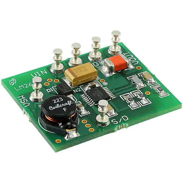
AN-1147 LM2651_EVAL
1.5A High Efficiency Synchronous Switching Regulator
Evaluation Board
1
Introduction
The LM2651 switching regulator provides high efficiency power conversion over a 100:1 load range (1.5A
to 15mA). This feature makes the LM2651 an ideal fit in battery powered applications.
Synchronous rectification and 75 mΩ internal switches provide up to 97% efficiency. At light loads, the
LM2651 enters a low power hysteretic or sleep mode to keep the efficiency high. In many applications, the
efficiency still exceeds 80% at 15 mA load.
A shutdown pin is available to disable the LM2651 and reduce the supply current to 7 µA. The IC contains
patented current sensing circuitry for current mode control. This feature eliminates the external current
sensing required by other current mode DC to DC converters. The IC has a 300kHz fixed frequency
internal oscillator. The high oscillator frequency allows the use of extremely small, low profile components.
The evaluation board can be obtained by ordering part number LM2651_EVAL from your local Texas
Instruments sales office, or TI website at www.ti.com.
2
Evaluation Board Design
The evaluation board is designed to supply 1.8V, 2.5V, 3.3V or adjustable output voltages at 15 mA up to
1.5A. The evaluation board comes with a design to supply an output voltage of 2.5V with input voltage
range of 4V to 14V and output current range of 15 mA to 1.5A. The design can easily be modified to
provide other output voltage using Equation 1 to change the ratio of the feedback resistors R1 and R2:
R1 = R2
VOUT
-1
1.238
(1)
The feedback resistors should not be made arbitrarily large as this would create a high impedance node at
the feedback pin that is more susceptible to noise. A combined value of 50 kΩ for the two resistors is
adequate.
Components were selected based on the design procedure in the LM2651 datasheet. PCB layout is
critical to reduce noise and ensure specified performance for any power supply design. To minimize the
parasitic inductance in the loop of input capacitors and the internal MOSFETs, connect the capacitors to
VIN and PGND pins with short and wide traces. This is important because the rapidly switching current,
together with wiring inductance can generate large voltage spikes that may cause noise problems. Locate
the feedback resistors close to the IC and keep the feedback trace as short as possible. Do not run any
feedback traces near the switch node and keep away from the flux field of the inductor. The schematic is
shown in Figure 1. The parts list of the design is shown in Table 1. The pictorial representations of the
layout top, bottom and silkscreen layers are shown at the end of this application note.
When an undervoltage situation occurs, the output voltage can be pulled below ground as the inductor
current is reversed through the synchronous FET. For applications which need to be protected from a
negative voltage, a clamping diode D2 is recommended. When used, D2 should be connected cathode to
VOUT and anode to ground. A diode rated for a minimum of 2A is recommended.
All trademarks are the property of their respective owners.
SNVA019A – October 2007 – Revised April 2013
Submit Documentation Feedback
AN-1147 LM2651_EVAL 1.5A High Efficiency Synchronous Switching
Regulator Evaluation Board
Copyright © 2007–2013, Texas Instruments Incorporated
1
�Operating the Evaluation Board
www.ti.com
Figure 1. LM2651_EVAL Schematic for Adjustable Voltage
Table 1. Bill of Materials
Ref Designator
Part Description
Part Number
U1
IC LM2651MTC-ADJ
LM2651MTC-ADJ
L1
Inductor
Coilcraft DO3316P-223
CIN
Tan Cap 100 µF 16V 10% Size = D
Vishay 594D107X0016D2T
CSS
Cer Cap 4.7 nF 50V X7R 10% 1206
Vishay VJ1206Y472KXAMB
CC2
Cer Cap 100 pF 50V NPO 1206
Vishay VJ1206A101JXAMB
CC1
Cer Cap 2.2 nF 50V X7R 10% 1206
Vishay VJ1206Y222KXAMB
COUT
Tan Cap 120 µF 6.3V 10% Size = D
Vishay 594D127X06R3C2T
CIN2
Cer Cap 0.1 µF 50V X7R 10% 0805
Vishay VJ0805Y104KXAMB
CB
Cer Cap 0.1 µF 50V X7R 10% 0805
Vishay VJ0805Y104KXAMB
R1
Res 20.0 kΩ ⅛W 1% 0805
Vishay CRCW08052002F
R2
Res 19.6 kΩ ⅛W 1% 0805
Vishay CRCW08051962F
RC
Res 30.0 kΩ ⅛W 5% 0805
Vishay CRCW0805303J
D1
Schottky Diode 1A SMA
Motorola MBRA130LT3
3
Operating the Evaluation Board
3.1
Setup
The LM2651_EVAL evaluation board comes ready to be tested. The only setup needed is connecting the
input voltage to the VIN and GND posts. The load and output are connected to the VOUT post.
3.2
Operating Conditions
The input voltage to the LM2651 regulator must be within the range of 4V to 14V DC for proper operation.
The device will not function properly with voltages below 4V and damage may occur if any voltage greater
than 16V is applied. Refer to LM2651 1.5A High Efficiency Synchronous Switching Regulator (SNVS032)
for all performance characteristics.
2
AN-1147 LM2651_EVAL 1.5A High Efficiency Synchronous Switching
Regulator Evaluation Board
SNVA019A – October 2007 – Revised April 2013
Submit Documentation Feedback
Copyright © 2007–2013, Texas Instruments Incorporated
�Layouts
www.ti.com
4
Layouts
Figure 2. Layout Top Layer
Figure 3. Layout Bottom Layer
Figure 4. Layout Silkscreen
SNVA019A – October 2007 – Revised April 2013
Submit Documentation Feedback
AN-1147 LM2651_EVAL 1.5A High Efficiency Synchronous Switching
Regulator Evaluation Board
Copyright © 2007–2013, Texas Instruments Incorporated
3
�IMPORTANT NOTICE
Texas Instruments Incorporated and its subsidiaries (TI) reserve the right to make corrections, enhancements, improvements and other
changes to its semiconductor products and services per JESD46, latest issue, and to discontinue any product or service per JESD48, latest
issue. Buyers should obtain the latest relevant information before placing orders and should verify that such information is current and
complete. All semiconductor products (also referred to herein as “components”) are sold subject to TI’s terms and conditions of sale
supplied at the time of order acknowledgment.
TI warrants performance of its components to the specifications applicable at the time of sale, in accordance with the warranty in TI’s terms
and conditions of sale of semiconductor products. Testing and other quality control techniques are used to the extent TI deems necessary
to support this warranty. Except where mandated by applicable law, testing of all parameters of each component is not necessarily
performed.
TI assumes no liability for applications assistance or the design of Buyers’ products. Buyers are responsible for their products and
applications using TI components. To minimize the risks associated with Buyers’ products and applications, Buyers should provide
adequate design and operating safeguards.
TI does not warrant or represent that any license, either express or implied, is granted under any patent right, copyright, mask work right, or
other intellectual property right relating to any combination, machine, or process in which TI components or services are used. Information
published by TI regarding third-party products or services does not constitute a license to use such products or services or a warranty or
endorsement thereof. Use of such information may require a license from a third party under the patents or other intellectual property of the
third party, or a license from TI under the patents or other intellectual property of TI.
Reproduction of significant portions of TI information in TI data books or data sheets is permissible only if reproduction is without alteration
and is accompanied by all associated warranties, conditions, limitations, and notices. TI is not responsible or liable for such altered
documentation. Information of third parties may be subject to additional restrictions.
Resale of TI components or services with statements different from or beyond the parameters stated by TI for that component or service
voids all express and any implied warranties for the associated TI component or service and is an unfair and deceptive business practice.
TI is not responsible or liable for any such statements.
Buyer acknowledges and agrees that it is solely responsible for compliance with all legal, regulatory and safety-related requirements
concerning its products, and any use of TI components in its applications, notwithstanding any applications-related information or support
that may be provided by TI. Buyer represents and agrees that it has all the necessary expertise to create and implement safeguards which
anticipate dangerous consequences of failures, monitor failures and their consequences, lessen the likelihood of failures that might cause
harm and take appropriate remedial actions. Buyer will fully indemnify TI and its representatives against any damages arising out of the use
of any TI components in safety-critical applications.
In some cases, TI components may be promoted specifically to facilitate safety-related applications. With such components, TI’s goal is to
help enable customers to design and create their own end-product solutions that meet applicable functional safety standards and
requirements. Nonetheless, such components are subject to these terms.
No TI components are authorized for use in FDA Class III (or similar life-critical medical equipment) unless authorized officers of the parties
have executed a special agreement specifically governing such use.
Only those TI components which TI has specifically designated as military grade or “enhanced plastic” are designed and intended for use in
military/aerospace applications or environments. Buyer acknowledges and agrees that any military or aerospace use of TI components
which have not been so designated is solely at the Buyer's risk, and that Buyer is solely responsible for compliance with all legal and
regulatory requirements in connection with such use.
TI has specifically designated certain components as meeting ISO/TS16949 requirements, mainly for automotive use. In any case of use of
non-designated products, TI will not be responsible for any failure to meet ISO/TS16949.
Products
Applications
Audio
www.ti.com/audio
Automotive and Transportation
www.ti.com/automotive
Amplifiers
amplifier.ti.com
Communications and Telecom
www.ti.com/communications
Data Converters
dataconverter.ti.com
Computers and Peripherals
www.ti.com/computers
DLP® Products
www.dlp.com
Consumer Electronics
www.ti.com/consumer-apps
DSP
dsp.ti.com
Energy and Lighting
www.ti.com/energy
Clocks and Timers
www.ti.com/clocks
Industrial
www.ti.com/industrial
Interface
interface.ti.com
Medical
www.ti.com/medical
Logic
logic.ti.com
Security
www.ti.com/security
Power Mgmt
power.ti.com
Space, Avionics and Defense
www.ti.com/space-avionics-defense
Microcontrollers
microcontroller.ti.com
Video and Imaging
www.ti.com/video
RFID
www.ti-rfid.com
OMAP Applications Processors
www.ti.com/omap
TI E2E Community
e2e.ti.com
Wireless Connectivity
www.ti.com/wirelessconnectivity
Mailing Address: Texas Instruments, Post Office Box 655303, Dallas, Texas 75265
Copyright © 2013, Texas Instruments Incorporated
�