LM2678
www.ti.com
SNVS029I – MARCH 2000 – REVISED APRIL 2013
LM2678 SIMPLE SWITCHER® High Efficiency 5A Step-Down Voltage Regulator
Check for Samples: LM2678
FEATURES
DESCRIPTION
•
•
The LM2678 series of regulators are monolithic
integrated circuits which provide all of the active
functions for a step-down (buck) switching regulator
capable of driving up to 5A loads with excellent line
and load regulation characteristics. High efficiency
(>90%) is obtained through the use of a low ONresistance DMOS power switch. The series consists
of fixed output voltages of 3.3V, 5V and 12V and an
adjustable output version.
1
23
•
•
•
•
•
•
•
Efficiency Up to 92%
Simple and Easy to Design with (Using OffThe-Shelf External Components)
120 mΩ DMOS Output Switch
3.3V, 5V and 12V Fixed Output and Adjustable
(1.2V to 37V ) Versions
50μA Standby Current When Switched OFF
±2% Maximum Output Tolerance Over Full
Line and Load Conditions
Wide Input Voltage Range: 8V to 40V
260 KHz Fixed Frequency Internal Oscillator
−40 to +125°C Operating Junction Temperature
Range
APPLICATIONS
•
•
•
Simple to Design, High Efficiency (>90%) StepDown Switching Regulators
Efficient System Pre-Regulator for Linear
Voltage Regulators
Battery Chargers
The SIMPLE SWITCHER® concept provides for a
complete design using a minimum number of external
components. A high fixed frequency oscillator
(260KHz) allows the use of physically smaller sized
components. A family of standard inductors for use
with the LM2678 are available from several
manufacturers to greatly simplify the design process.
The LM2678 series also has built in thermal
shutdown, current limiting and an ON/OFF control
input that can power down the regulator to a low
50μA quiescent current standby condition. The output
voltage is ensured to a ±2% tolerance. The clock
frequency is controlled to within a ±11% tolerance.
Typical Application
1
2
3
Please be aware that an important notice concerning availability, standard warranty, and use in critical applications of
Texas Instruments semiconductor products and disclaimers thereto appears at the end of this data sheet.
SIMPLE SWITCHER, Switchers Made Simple are registered trademarks of Texas Instruments.
All other trademarks are the property of their respective owners.
PRODUCTION DATA information is current as of publication date.
Products conform to specifications per the terms of the Texas
Instruments standard warranty. Production processing does not
necessarily include testing of all parameters.
Copyright © 2000–2013, Texas Instruments Incorporated
�LM2678
SNVS029I – MARCH 2000 – REVISED APRIL 2013
www.ti.com
Connection Diagrams
Top View
Top View
Figure 1. DDPAK Package
See Package Number KTW0007B
Figure 2. TO-220 Package
See Package Number NDZ0007B
Top View
*
1
14
VSW
VIN
2
13
VSW
VIN
3
12
VSW
CB
4
11
*
*
5
10
*
*
6
9
GND
FB
7
8
ON/OFF
DAP**
* No Connections
** Connect to Pin 9 on PCB
Figure 3. VSON-14 Package
See Package Number NHM0014A
These devices have limited built-in ESD protection. The leads should be shorted together or the device placed in conductive foam
during storage or handling to prevent electrostatic damage to the MOS gates.
Absolute Maximum Ratings
(1) (2)
Input Supply Voltage
45V
ON/OFF Pin Voltage
−0.1V to 6V
Switch Voltage to Ground
(3)
−1V to VIN
Boost Pin Voltage
VSW + 8V
−0.3V to 14V
Feedback Pin Voltage
Power Dissipation
ESD
Internally Limited
(4)
2 kV
−65°C to 150°C
Storage Temperature Range
Soldering Temperature
(1)
(2)
(3)
(4)
2
Wave
4 sec, 260°C
Infrared
10 sec, 240°C
Vapor Phase
75 sec, 219°C
Absolute Maximum Ratings are limits beyond which damage to the device may occur. Operating Ratings indicate conditions under
which of the device is ensured. Operating Ratings do not imply ensured performance limits. For ensured performance limits and
associated test condition, see the Electrical Characteristics tables.
If Military/Aerospace specified devices are required, please contact the Texas Instruments Sales Office/Distributors for availability and
specifications.
The absolute maximum specification of the 'Switch Voltage to Ground' applies to DC voltage. An extended negative voltage limit of -10V
applies to a pulse of up to 20 ns, -6V of 60 ns and -3V of up to 100 ns.
ESD was applied using the human-body model, a 100pF capacitor discharged through a 1.5 kΩ resistor into each pin.
Submit Documentation Feedback
Copyright © 2000–2013, Texas Instruments Incorporated
Product Folder Links: LM2678
�LM2678
www.ti.com
SNVS029I – MARCH 2000 – REVISED APRIL 2013
Operating Ratings
Supply Voltage
8V to 40V
−40°C to 125°C
Junction Temperature Range (TJ)
Electrical Characteristics
LM2678-3.3
Limits appearing in bold type face apply over the entire junction temperature range of operation, −40°C to 125°C.
Specifications appearing in normal type apply for TA = TJ = 25°C.
Parameter
Test Conditions
Typ (1)
Min (2)
Max (2)
Units
3.234/3.201
3.366/3.399
V
VOUT
Output Voltage
VIN = 8V to 40V, 100mA ≤ IOUT ≤ 5A
3.3
η
Efficiency
VIN = 12V, ILOAD = 5A
82
(1)
(2)
%
Typical values are determined with TA = TJ = 25°C and represent the most likely norm.
All limits are ensured at room temperature (standard type face) and at temperature extremes (bold type face). All room temperature
limits are 100% tested during production with TA = TJ = 25°C. All limits at temperature extremes are ensured via correlation using
standard Quality Control (SQC) methods. All limits are used to calculate Average Outgoing Quality Level (AOQL).
LM2678-5.0
Parameter
Test Conditions
Typ (1)
Min (2)
Max (2)
4.900/4.850
5.100/5.150
VOUT
Output Voltage
VIN = 8V to 40V, 100mA ≤ IOUT ≤ 5A
5.0
η
Efficiency
VIN = 12V, ILOAD = 5A
84
(1)
(2)
Units
V
%
Typical values are determined with TA = TJ = 25°C and represent the most likely norm.
All limits are ensured at room temperature (standard type face) and at temperature extremes (bold type face). All room temperature
limits are 100% tested during production with TA = TJ = 25°C. All limits at temperature extremes are ensured via correlation using
standard Quality Control (SQC) methods. All limits are used to calculate Average Outgoing Quality Level (AOQL).
LM2678-12
Parameter
Test Conditions
Typ (1)
Min (2)
Max (2)
Units
11.76/11.64
12.24/12.36
V
VOUT
Output Voltage
VIN = 15V to 40V, 100mA ≤ IOUT ≤ 5A
12
η
Efficiency
VIN = 24V, ILOAD = 5A
92
(1)
(2)
%
Typical values are determined with TA = TJ = 25°C and represent the most likely norm.
All limits are ensured at room temperature (standard type face) and at temperature extremes (bold type face). All room temperature
limits are 100% tested during production with TA = TJ = 25°C. All limits at temperature extremes are ensured via correlation using
standard Quality Control (SQC) methods. All limits are used to calculate Average Outgoing Quality Level (AOQL).
LM2678-ADJ
Parameter
Test Conditions
VFB
Feedback Voltage
VIN = 8V to 40V, 100mA ≤ IOUT ≤ 5A
VOUT Programmed for 5V
η
Efficiency
VIN = 12V, ILOAD = 5A
(1)
(2)
Typ (1)
Min (2)
Max (2)
Units
1.21
1.186/1.174
1.234/1.246
V
84
%
Typical values are determined with TA = TJ = 25°C and represent the most likely norm.
All limits are ensured at room temperature (standard type face) and at temperature extremes (bold type face). All room temperature
limits are 100% tested during production with TA = TJ = 25°C. All limits at temperature extremes are ensured via correlation using
standard Quality Control (SQC) methods. All limits are used to calculate Average Outgoing Quality Level (AOQL).
Submit Documentation Feedback
Copyright © 2000–2013, Texas Instruments Incorporated
Product Folder Links: LM2678
3
�LM2678
SNVS029I – MARCH 2000 – REVISED APRIL 2013
www.ti.com
All Output Voltage Versions
Electrical Characteristics
Limits appearing in bold type face apply over the entire junction temperature range of operation, −40°C to 125°C.
Specifications appearing in normal type apply for TA = TJ = 25°C. Unless otherwise specified VIN=12V for the 3.3V, 5V and
Adjustable versions and VIN=24V for the 12V version.
Parameter
Test Conditions
Typ
Min
Max
Units
4.2
6
mA
50
100/150
μA
8.3/8.75
A
DEVICE PARAMETERS
IQ
Quiescent Current
VFEEDBACK = 8V
For 3.3V, 5.0V, and ADJ Versions
VFEEDBACK = 15V
For 12V Versions
ISTBY
Standby Quiescent
Current
ICL
Current Limit
IL
Output Leakage Current
ON/OFF Pin = 0V
7
VIN = 40V, ON/OFF Pin = 0V,
VSWITCH = 0V,
VSWITCH = −1V
6.1/5.75
200
15
16
μA
mA
0.14/0.225
Ω
280
kHz
RDS(ON)
Switch On-Resistance
ISWITCH = 5A
0.12
fO
Oscillator Frequency
Measured at Switch Pin
260
D
Duty Cycle
Maximum Duty Cycle
91
Minimum Duty Cycle
0
%
VFEEDBACK = 1.3V ADJ Version Only
85
nA
IBIAS
Feedback Bias Current
VON/OFF
ON/OFF Threshold
Voltage
ION/OFF
ON/OFF Input Current
ON/OFF Input = 0V
20
θJA
Thermal Resistance
T Package, Junction to Ambient (1)
65
θJA
T Package, Junction to Ambient (2)
45
θJC
T Package, Junction to Case
2
θJA
S Package, Junction to Ambient (3)
56
θJA
S Package, Junction to Ambient (4)
35
θJA
S Package, Junction to Ambient (5)
26
θJC
S Package, Junction to Case
2
θJA
SD Package, Junction to Ambient (6)
55
θJA
SD Package, Junction to Ambient (7)
29
(1)
(2)
(3)
(4)
(5)
(6)
(7)
4
1.4
225
%
0.8
2.0
V
45
μA
°C/W
++
°C/W
Junction to ambient thermal resistance (no external heat sink) for the 7 lead TO-220 package mounted vertically, with ½ inch leads in a
socket, or on a PC board with minimum copper area.
Junction to ambient thermal resistance (no external heat sink) for the 7 lead TO-220 package mounted vertically, with ½ inch leads
soldered to a PC board containing approximately 4 square inches of (1 oz.) copper area surrounding the leads.
Junction to ambient thermal resistance for the 7 lead DDPAK mounted horizontally against a PC board area of 0.136 square inches (the
same size as the DDPAK package) of 1 oz. (0.0014 in. thick) copper.
Junction to ambient thermal resistance for the 7 lead DDPAK mounted horizontally against a PC board area of 0.4896 square inches
(3.6 times the area of the DDPAK package) of 1 oz. (0.0014 in. thick) copper.
Junction to ambient thermal resistance for the 7 lead DDPAK mounted horizontally against a PC board copper area of 1.0064 square
inches (7.4 times the area of the DDPAK package) of 1 oz. (0.0014 in. thick) copper. Additional copper area will reduce thermal
resistance further. See the thermal model in Switchers Made Simple® software.
Junction to ambient thermal resistance for the 14-lead VSON mounted on a PC board copper area equal to the die attach paddle.
Junction to ambient thermal resistance for the 14-lead VSON mounted on a PC board copper area using 12 vias to a second layer of
copper equal to die attach paddle. Additional copper area will reduce thermal resistance further. For layout recommendations, refer to
Application Note AN-1187 at www.ti.com/lsds/ti/analog/powermanagement/power_portal.page.
Submit Documentation Feedback
Copyright © 2000–2013, Texas Instruments Incorporated
Product Folder Links: LM2678
�LM2678
www.ti.com
SNVS029I – MARCH 2000 – REVISED APRIL 2013
Typical Performance Characteristics
Normalized Output Voltage
Line Regulation
Figure 4.
Figure 5.
Efficiency vs Input Voltage
Efficiency vs ILOAD
Figure 6.
Figure 7.
Switch Current Limit
Operating Quiescent Current
Figure 8.
Figure 9.
Submit Documentation Feedback
Copyright © 2000–2013, Texas Instruments Incorporated
Product Folder Links: LM2678
5
�LM2678
SNVS029I – MARCH 2000 – REVISED APRIL 2013
www.ti.com
Typical Performance Characteristics (continued)
Standby Quiescent Current
ON/OFF Threshold Voltage
Figure 10.
Figure 11.
ON/OFF Pin Current (Sourcing)
Switching Frequency
Figure 12.
Figure 13.
Feedback Pin Bias Current
Continuous Mode Switching Waveforms
VIN = 20V, VOUT = 5V, ILOAD = 5A
L = 10 μH, COUT = 400 μF, COUTESR = 13 mΩ
Figure 14.
6
A. VSW Pin Voltage, 10 V/div.
B. Inductor Current, 2 A/div
C. Output Ripple Voltage, 20 mV/div AC-Coupled
Figure 15. Horizontal Time Base: 1 μs/div
Submit Documentation Feedback
Copyright © 2000–2013, Texas Instruments Incorporated
Product Folder Links: LM2678
�LM2678
www.ti.com
SNVS029I – MARCH 2000 – REVISED APRIL 2013
Typical Performance Characteristics (continued)
Discontinuous Mode Switching Waveforms
VIN = 20V, VOUT = 5V, ILOAD = 500 mA
L = 10 μH, COUT = 400 μF, COUTESR = 13 mΩ
A. VSW Pin Voltage, 10 V/div.
B. Inductor Current, 1 A/div
C. Output Ripple Voltage, 20 mV/div AC-Coupled
Figure 16. Horizontal Time Base: 1 μs//iv
Load Transient Response for Continuous Mode
VIN = 20V, VOUT = 5V
L = 10 μH, COUT = 400 μF, COUTESR = 13 mΩ
A. Output Voltage, 100 mV//div, AC-Coupled.
B. Load Current: 500 mA to 5A Load Pulse
Figure 17. Horizontal Time Base: 100 μs/div
Load Transient Response for Discontinuous Mode
VIN = 20V, VOUT = 5V, vs
L = 10 μH, COUT = 400 μF, COUTESR = 13 mΩ
A. Output Voltage, 100 mV/div, AC-Coupled.
B. Load Current: 200 mA to 3A Load Pulse
Figure 18. Horizontal Time Base: 200 μs/div
Submit Documentation Feedback
Copyright © 2000–2013, Texas Instruments Incorporated
Product Folder Links: LM2678
7
�LM2678
SNVS029I – MARCH 2000 – REVISED APRIL 2013
www.ti.com
Block Diagram
* Active Inductor Patent Number 5,514,947
† Active Capacitor Patent Number 5,382,918
8
Submit Documentation Feedback
Copyright © 2000–2013, Texas Instruments Incorporated
Product Folder Links: LM2678
�LM2678
www.ti.com
SNVS029I – MARCH 2000 – REVISED APRIL 2013
APPLICATION HINTS
The LM2678 provides all of the active functions required for a step-down (buck) switching regulator. The internal
power switch is a DMOS power MOSFET to provide power supply designs with high current capability, up to 5A,
and highly efficient operation.
The LM2678 is part of the SIMPLE SWITCHER® family of power converters. A complete design uses a minimum
number of external components, which have been pre-determined from a variety of manufacturers . Using either
this data sheet or a design software program called LM267X Made Simple (version 2.0) a complete switching
power supply can be designed quickly. The software is provided free of charge and can be downloaded from
Texas Instrument's Internet site located at http://www.ti.com.
SWITCH OUTPUT
This is the output of a power MOSFET switch connected directly to the input voltage. The switch provides energy
to an inductor, an output capacitor and the load circuitry under control of an internal pulse-width-modulator
(PWM). The PWM controller is internally clocked by a fixed 260KHz oscillator. In a standard step-down
application the duty cycle (Time ON/Time OFF) of the power switch is proportional to the ratio of the power
supply output voltage to the input voltage. The voltage on pin 1 switches between Vin (switch ON) and below
ground by the voltage drop of the external Schottky diode (switch OFF).
INPUT
The input voltage for the power supply is connected to pin 2. In addition to providing energy to the load the input
voltage also provides bias for the internal circuitry of the LM2678. For ensured performance the input voltage
must be in the range of 8V to 40V. For best performance of the power supply the input pin should always be
bypassed with an input capacitor located close to pin 2.
C BOOST
A capacitor must be connected from pin 3 to the switch output, pin 1. This capacitor boosts the gate drive to the
internal MOSFET above Vin to fully turn it ON. This minimizes conduction losses in the power switch to maintain
high efficiency. The recommended value for C Boost is 0.01μF.
GROUND
This is the ground reference connection for all components in the power supply. In fast-switching, high-current
applications such as those implemented with the LM2678, it is recommended that a broad ground plane be used
to minimize signal coupling throughout the circuit
FEEDBACK
This is the input to a two-stage high gain amplifier, which drives the PWM controller. It is necessary to connect
pin 6 to the actual output of the power supply to set the dc output voltage. For the fixed output devices (3.3V, 5V
and 12V outputs), a direct wire connection to the output is all that is required as internal gain setting resistors are
provided inside the LM2678. For the adjustable output version two external resistors are required to set the dc
output voltage. For stable operation of the power supply it is important to prevent coupling of any inductor flux to
the feedback input.
ON/OFF
This input provides an electrical ON/OFF control of the power supply. Connecting this pin to ground or to any
voltage less than 0.8V will completely turn OFF the regulator. The current drain from the input supply when OFF
is only 50μA. Pin 7 has an internal pull-up current source of approximately 20μA and a protection clamp zener
diode of 7V to ground. When electrically driving the ON/OFF pin the high voltage level for the ON condition
should not exceed the 6V absolute maximum limit. When ON/OFF control is not required pin 7 should be left
open circuited.
DAP (VSON PACKAGE)
The Die Attach Pad (DAP) can and should be connected to PCB Ground plane/island. For CAD and assembly
guidelines refer to Application Note AN-1187 at www.ti.com/lsds/ti/analog/powermanagement/power_portal.page.
Submit Documentation Feedback
Copyright © 2000–2013, Texas Instruments Incorporated
Product Folder Links: LM2678
9
�LM2678
SNVS029I – MARCH 2000 – REVISED APRIL 2013
www.ti.com
DESIGN CONSIDERATIONS
Figure 19. Basic Circuit for Fixed Output Voltage Applications.
Figure 20. Basic Circuit for Adjustable Output Voltage Applications
Power supply design using the LM2678 is greatly simplified by using recommended external components. A wide
range of inductors, capacitors and Schottky diodes from several manufacturers have been evaluated for use in
designs that cover the full range of capabilities (input voltage, output voltage and load current) of the LM2678. A
simple design procedure using nomographs and component tables provided in this data sheet leads to a working
design with very little effort. Alternatively, the design software, LM267X Made Simple (version 6.0), can also be
used to provide instant component selection, circuit performance calculations for evaluation, a bill of materials
component list and a circuit schematic.
The individual components from the various manufacturers called out for use are still just a small sample of the
vast array of components available in the industry. While these components are recommended, they are not
exclusively the only components for use in a design. After a close comparison of component specifications,
equivalent devices from other manufacturers could be substituted for use in an application.
Important considerations for each external component and an explanation of how the nomographs and selection
tables were developed follows.
10
Submit Documentation Feedback
Copyright © 2000–2013, Texas Instruments Incorporated
Product Folder Links: LM2678
�LM2678
www.ti.com
SNVS029I – MARCH 2000 – REVISED APRIL 2013
INDUCTOR
The inductor is the key component in a switching regulator. For efficiency the inductor stores energy during the
switch ON time and then transfers energy to the load while the switch is OFF.
Nomographs are used to select the inductance value required for a given set of operating conditions. The
nomographs assume that the circuit is operating in continuous mode (the current flowing through the inductor
never falls to zero). The magnitude of inductance is selected to maintain a maximum ripple current of 30% of the
maximum load current. If the ripple current exceeds this 30% limit the next larger value is selected.
The inductors offered have been specifically manufactured to provide proper operation under all operating
conditions of input and output voltage and load current. Several part types are offered for a given amount of
inductance. Both surface mount and through-hole devices are available. The inductors from each of the three
manufacturers have unique characteristics.
Renco: ferrite stick core inductors; benefits are typically lowest cost and can withstand ripple and transient peak
currents above the rated value. These inductors have an external magnetic field, which may generate EMI.
Pulse Engineering: powdered iron toroid core inductors; these also can withstand higher than rated currents and,
being toroid inductors, will have low EMI.
Coilcraft: ferrite drum core inductors; these are the smallest physical size inductors and are available only as
surface mount components. These inductors also generate EMI but less than stick inductors.
OUTPUT CAPACITOR
The output capacitor acts to smooth the dc output voltage and also provides energy storage. Selection of an
output capacitor, with an associated equivalent series resistance (ESR), impacts both the amount of output ripple
voltage and stability of the control loop.
The output ripple voltage of the power supply is the product of the capacitor ESR and the inductor ripple current.
The capacitor types recommended in the tables were selected for having low ESR ratings.
In addition, both surface mount tantalum capacitors and through-hole aluminum electrolytic capacitors are offered
as solutions.
Impacting frequency stability of the overall control loop, the output capacitance, in conjunction with the inductor,
creates a double pole inside the feedback loop. In addition the capacitance and the ESR value create a zero.
These frequency response effects together with the internal frequency compensation circuitry of the LM2678
modify the gain and phase shift of the closed loop system.
As a general rule for stable switching regulator circuits it is desired to have the unity gain bandwidth of the circuit
to be limited to no more than one-sixth of the controller switching frequency. With the fixed 260KHz switching
frequency of the LM2678, the output capacitor is selected to provide a unity gain bandwidth of 40KHz maximum.
Each recommended capacitor value has been chosen to achieve this result.
In some cases multiple capacitors are required either to reduce the ESR of the output capacitor, to minimize
output ripple (a ripple voltage of 1% of Vout or less is the assumed performance condition), or to increase the
output capacitance to reduce the closed loop unity gain bandwidth (to less than 40KHz). When parallel
combinations of capacitors are required it has been assumed that each capacitor is the exact same part type.
The RMS current and working voltage (WV) ratings of the output capacitor are also important considerations. In a
typical step-down switching regulator, the inductor ripple current (set to be no more than 30% of the maximum
load current by the inductor selection) is the current that flows through the output capacitor. The capacitor RMS
current rating must be greater than this ripple current. The voltage rating of the output capacitor should be
greater than 1.3 times the maximum output voltage of the power supply. If operation of the system at elevated
temperatures is required, the capacitor voltage rating may be de-rated to less than the nominal room temperature
rating. Careful inspection of the manufacturer's specification for de-rating of working voltage with temperature is
important.
Submit Documentation Feedback
Copyright © 2000–2013, Texas Instruments Incorporated
Product Folder Links: LM2678
11
�LM2678
SNVS029I – MARCH 2000 – REVISED APRIL 2013
www.ti.com
INPUT CAPACITOR
Fast changing currents in high current switching regulators place a significant dynamic load on the unregulated
power source. An input capacitor helps to provide additional current to the power supply as well as smooth out
input voltage variations.
Like the output capacitor, the key specifications for the input capacitor are RMS current rating and working
voltage. The RMS current flowing through the input capacitor is equal to one-half of the maximum dc load current
so the capacitor should be rated to handle this. Paralleling multiple capacitors proportionally increases the
current rating of the total capacitance. The voltage rating should also be selected to be 1.3 times the maximum
input voltage. Depending on the unregulated input power source, under light load conditions the maximum input
voltage could be significantly higher than normal operation and should be considered when selecting an input
capacitor.
The input capacitor should be placed very close to the input pin of the LM2678. Due to relative high current
operation with fast transient changes, the series inductance of input connecting wires or PCB traces can create
ringing signals at the input terminal which could possibly propagate to the output or other parts of the circuitry. It
may be necessary in some designs to add a small valued (0.1μF to 0.47μF) ceramic type capacitor in parallel
with the input capacitor to prevent or minimize any ringing.
CATCH DIODE
When the power switch in the LM2678 turns OFF, the current through the inductor continues to flow. The path for
this current is through the diode connected between the switch output and ground. This forward biased diode
clamps the switch output to a voltage less than ground. This negative voltage must be greater than −1V so a low
voltage drop (particularly at high current levels) Schottky diode is recommended. Total efficiency of the entire
power supply is significantly impacted by the power lost in the output catch diode. The average current through
the catch diode is dependent on the switch duty cycle (D) and is equal to the load current times (1-D). Use of a
diode rated for much higher current than is required by the actual application helps to minimize the voltage drop
and power loss in the diode.
During the switch ON time the diode will be reversed biased by the input voltage. The reverse voltage rating of
the diode should be at least 1.3 times greater than the maximum input voltage.
BOOST CAPACITOR
The boost capacitor creates a voltage used to overdrive the gate of the internal power MOSFET. This improves
efficiency by minimizing the on resistance of the switch and associated power loss. For all applications it is
recommended to use a 0.01μF/50V ceramic capacitor.
ADDITIONAL APPLICATION INFORMATION
When the output voltage is greater than approximately 6V, and the duty cycle at minimum input voltage is greater
than approximately 50%, the designer should exercise caution in selection of the output filter components. When
an application designed to these specific operating conditions is subjected to a current limit fault condition, it may
be possible to observe a large hysteresis in the current limit. This can affect the output voltage of the device until
the load current is reduced sufficiently to allow the current limit protection circuit to reset itself.
Under current limiting conditions, the LM267x is designed to respond in the following manner:
1. At the moment when the inductor current reaches the current limit threshold, the ON-pulse is immediately
terminated. This happens for any application condition.
2. However, the current limit block is also designed to momentarily reduce the duty cycle to below 50% to avoid
subharmonic oscillations, which could cause the inductor to saturate.
3. Thereafter, once the inductor current falls below the current limit threshold, there is a small relaxation time
during which the duty cycle progressively rises back above 50% to the value required to achieve regulation.
If the output capacitance is sufficiently ‘large’, it may be possible that as the output tries to recover, the output
capacitor charging current is large enough to repeatedly re-trigger the current limit circuit before the output has
fully settled. This condition is exacerbated with higher output voltage settings because the energy requirement of
the output capacitor varies as the square of the output voltage (½CV2), thus requiring an increased charging
current.
12
Submit Documentation Feedback
Copyright © 2000–2013, Texas Instruments Incorporated
Product Folder Links: LM2678
�LM2678
www.ti.com
SNVS029I – MARCH 2000 – REVISED APRIL 2013
A simple test to determine if this condition might exist for a suspect application is to apply a short circuit across
the output of the converter, and then remove the shorted output condition. In an application with properly
selected external components, the output will recover smoothly.
Practical values of external components that have been experimentally found to work well under these specific
operating conditions are COUT = 47µF, L = 22µH. It should be noted that even with these components, for a
device’s current limit of ICLIM, the maximum load current under which the possibility of the large current limit
hysteresis can be minimized is ICLIM/2. For example, if the input is 24V and the set output voltage is 18V, then for
a desired maximum current of 1.5A, the current limit of the chosen switcher must be confirmed to be at least 3A.
Under extreme over-current or short circuit conditions, the LM267X employs frequency foldback in addition to the
current limit. If the cycle-by-cycle inductor current increases above the current limit threshold (due to short circuit
or inductor saturation for example) the switching frequency will be automatically reduced to protect the IC.
Frequency below 100 KHz is typical for an extreme short circuit condition.
SIMPLE DESIGN PROCEDURE
Using the nomographs and tables in this data sheet (or use the available design software at www.ti.com) a
complete step-down regulator can be designed in a few simple steps.
Step 1: Define the power supply operating conditions:
Required output voltage
Maximum DC input voltage
Maximum output load current
Step 2: Set the output voltage by selecting a fixed output LM2678 (3.3V, 5V or 12V applications) or determine
the required feedback resistors for use with the adjustable LM2678−ADJ
Step 3: Determine the inductor required by using one of the four nomographs, Figure 21 through Figure 24.
Table 1 provides a specific manufacturer and part number for the inductor.
Step 4: Using Table 6 (fixed output voltage) or Table 12 (adjustable output voltage), determine the output
capacitance required for stable operation. Table 3 provides the specific capacitor type from the manufacturer of
choice.
Step 5: Determine an input capacitor from Table 6 for fixed output voltage applications. Use Table 3 to find the
specific capacitor type. For adjustable output circuits select a capacitor from Table 3 with a sufficient working
voltage (WV) rating greater than Vin max, and an rms current rating greater than one-half the maximum load
current (2 or more capacitors in parallel may be required).
Step 6: Select a diode from Table 10. The current rating of the diode must be greater than I load max and the
Reverse Voltage rating must be greater than Vin max.
Step 7: Include a 0.01μF/50V capacitor for Cboost in the design.
FIXED OUTPUT VOLTAGE DESIGN EXAMPLE
A system logic power supply bus of 3.3V is to be generated from a wall adapter which provides an unregulated
DC voltage of 13V to 16V. The maximum load current is 4A. Through-hole components are preferred.
Step 1: Operating conditions are:
Vout = 3.3V
Vin max = 16V
Iload max = 4A
Step 2: Select an LM2678T-3.3. The output voltage will have a tolerance of
±2% at room temperature and ±3% over the full operating temperature range.
Step 3: Use the nomograph for the 3.3V device, Figure 21. The intersection of the 16V horizontal line (Vin max)
and the 4A vertical line (Iload max) indicates that L46, a 15μH inductor, is required.
From Table 1, L46 in a through-hole component is available from Renco with part number RL-1283-15-43.
Submit Documentation Feedback
Copyright © 2000–2013, Texas Instruments Incorporated
Product Folder Links: LM2678
13
�LM2678
SNVS029I – MARCH 2000 – REVISED APRIL 2013
www.ti.com
Step 4: Use Table 6 to determine an output capacitor. With a 3.3V output and a 15μH inductor there are four
through-hole output capacitor solutions with the number of same type capacitors to be paralleled and an
identifying capacitor code given. Table 3 provides the actual capacitor characteristics. Any of the following
choices will work in the circuit:
2 x 220μF/10V Sanyo OS-CON (code C5)
2 x 820μF/16V Sanyo MV-GX (code C5)
1 x 3900μF/10V Nichicon PL (code C7)
2 x 560μF/35V Panasonic HFQ (code C5)
Step 5: Use Table 6 to select an input capacitor. With 3.3V output and 15μH there are three through-hole
solutions. These capacitors provide a sufficient voltage rating and an rms current rating greater than 2A (1/2 Iload
max). Again using Table 3 for specific component characteristics the following choices are suitable:
2 x 680μF/63V Sanyo MV-GX (code C13)
1 x 1200μF/63V Nichicon PL (code C25)
1 x 1500μF/63V Panasonic HFQ (code C16)
Step 6: From Table 10 a 5A or more Schottky diode must be selected. For through-hole components only 40V
rated diodes are indicated and 4 part types are suitable:
1N5825
MBR745
80SQ045
6TQ045
Step 7: A 0.01μF capacitor will be used for Cboost.
ADJUSTABLE OUTPUT DESIGN EXAMPLE
In this example it is desired to convert the voltage from a two battery automotive power supply (voltage range of
20V to 28V, typical in large truck applications) to the 14.8VDC alternator supply typically used to power electronic
equipment from single battery 12V vehicle systems. The load current required is 3.5A maximum. It is also
desired to implement the power supply with all surface mount components.
Step 1: Operating conditions are:
Vout = 14.8V
Vin max = 28V
Iload max = 3.5A
Step 2: Select an LM2678S-ADJ. To set the output voltage to 14.9V two resistors need to be chosen (R1 and R2
in Figure 20). For the adjustable device the output voltage is set by the following relationship:
where
•
VFB is the feedback voltage of typically 1.21V
(1)
A recommended value to use for R1 is 1K. In this example then R2 is determined to be:
(2)
R2 = 11.23KΩ
The closest standard 1% tolerance value to use is 11.3KΩ
This will set the nominal output voltage to 14.88V which is within 0.5% of the target value.
14
Submit Documentation Feedback
Copyright © 2000–2013, Texas Instruments Incorporated
Product Folder Links: LM2678
�LM2678
www.ti.com
SNVS029I – MARCH 2000 – REVISED APRIL 2013
Step 3: To use the nomograph for the adjustable device, Figure 24, requires a calculation of the inductor
Volt•microsecond constant (E•T expressed in V•μS) from the following formula:
where
•
VSAT is the voltage drop across the internal power switch which is Rds(ON) times Iload
(3)
In this example this would be typically 0.12Ω x 3.5A or 0.42V and VD is the voltage drop across the forward
bisased Schottky diode, typically 0.5V. The switching frequency of 260KHz is the nominal value to use to
estimate the ON time of the switch during which energy is stored in the inductor.
For this example E•T is found to be:
(4)
(5)
Using Figure 24, the intersection of 27V•μS horizontally and the 3.5A vertical line (Iload max) indicates that L48 , a
47μH inductor, or L49, a 33μH inductor could be used. Either inductor will be suitable, but for this example
selecting the larger inductance will result in lower ripple current.
From Table 1, L48 in a surface mount component is available from Pulse Engineering with part number P0848.
Step 4: Use Table 12 to determine an output capacitor. With a 14.8V output the 12.5 to 15V row is used and with
a 47μH inductor there are three surface mount output capacitor solutions. Table 3 provides the actual capacitor
characteristics based on the C Code number. Any of the following choices can be used:
1 x 33μF/20V AVX TPS (code C6)
1 x 47μF/20V Sprague 594 (code C8)
1 x 47μF/20V Kemet T495 (code C8)
NOTE
When using the adjustable device in low voltage applications (less than 3V output), if the
nomograph, Figure 24, selects an inductance of 22μH or less, Table 12 and Table 13 do
not provide an output capacitor solution. With these conditions the number of output
capacitors required for stable operation becomes impractical. It is recommended to use
either a 33μH or 47μH inductor and the output capacitors from Table 12 and Table 13.
Step 5: An input capacitor for this example will require at least a 35V WV rating with an rms current rating of
1.75A (1/2 Iout max). From Table 3 it can be seen that C12, a 33μF/35V capacitor from Sprague, has the highest
voltage/current rating of the surface mount components and that two of these capacitor in parallel will be
adequate.
Step 6: From Table 10 a 5A or more Schottky diode must be selected. For surface mount diodes with a margin
of safety on the voltage rating one of two diodes can be used:
MBRD1545CT
6TQ045S
Step 7: A 0.01μF capacitor will be used for Cboost.
VSON PACKAGE DEVICES
The LM2678 is offered in the 14 lead VSON surface mount package to allow for a significantly decreased
footprint with equivalent power dissipation compared to the DDPAK. For details on mounting and soldering
specifications,
refer
to
Application
Note
AN-1187
at
www.ti.com/lsds/ti/analog/powermanagement/power_portal.page.
Submit Documentation Feedback
Copyright © 2000–2013, Texas Instruments Incorporated
Product Folder Links: LM2678
15
�LM2678
SNVS029I – MARCH 2000 – REVISED APRIL 2013
www.ti.com
Inductor Selection Guides
For Continuous Mode Operation
16
Figure 21. LM2678-3.3
Figure 22. LM2678-5.0
Figure 23. LM2678-12
Figure 24. LM2678-ADJ
Submit Documentation Feedback
Copyright © 2000–2013, Texas Instruments Incorporated
Product Folder Links: LM2678
�LM2678
www.ti.com
SNVS029I – MARCH 2000 – REVISED APRIL 2013
Table 1. Inductor Manufacturer Part Numbers
Inductor
Reference
Number
Inductance
(µH)
Current
(A)
L23
33
L24
22
L25
Renco
Pulse Engineering
Through Hole
Surface Mount
Coilcraft
Through Hole
Surface Mount
1.35
RL-5471-7
RL1500-33
PE-53823
PE-53823S
DO3316-333
1.65
RL-1283-22-43
RL1500-22
PE-53824
PE-53824S
DO3316-223
15
2.00
RL-1283-15-43
RL1500-15
PE-53825
PE-53825S
DO3316-153
L29
100
1.41
RL-5471-4
RL-6050-100
PE-53829
PE-53829S
DO5022P-104
L30
68
1.71
RL-5471-5
RL6050-68
PE-53830
PE-53830S
DO5022P-683
L31
47
2.06
RL-5471-6
RL6050-47
PE-53831
PE-53831S
DO5022P-473
L32
33
2.46
RL-5471-7
RL6050-33
PE-53932
PE-53932S
DO5022P-333
L33
22
3.02
RL-1283-22-43
RL6050-22
PE-53933
PE-53933S
DO5022P-223
L34
15
3.65
RL-1283-15-43
—
PE-53934
PE-53934S
DO5022P-153
L38
68
2.97
RL-5472-2
—
PE-54038
PE-54038S
—
L39
47
3.57
RL-5472-3
—
PE-54039
PE-54039S
—
L40
33
4.26
RL-1283-33-43
—
PE-54040
PE-54040S
—
L41
22
5.22
RL-1283-22-43
—
PE-54041
P0841
—
L44
68
3.45
RL-5473-3
—
PE-54044
L45
10
4.47
RL-1283-10-43
—
—
P0845
DO5022P-103HC
L46
15
5.60
RL-1283-15-43
—
—
P0846
DO5022P-153HC
L47
10
5.66
RL-1283-10-43
—
—
P0847
DO5022P-103HC
L48
47
5.61
RL-1282-47-43
—
—
P0848
—
L49
33
5.61
RL-1282-33-43
—
—
P0849
—
—
Surface Mount
—
Table 2. Inductor Manufacturer Contact Numbers
Coilcraft
Phone
(800) 322-2645
FAX
(708) 639-1469
Phone
+44 1236 730 595
FAX
+44 1236 730 627
Phone
(619) 674-8100
FAX
(619) 674-8262
Pulse Engineering,
Phone
+353 93 24 107
Europe
FAX
+353 93 24 459
Renco Electronics
Phone
(800) 645-5828
FAX
(516) 586-5562
Coilcraft, Europe
Pulse Engineering
Submit Documentation Feedback
Copyright © 2000–2013, Texas Instruments Incorporated
Product Folder Links: LM2678
17
�LM2678
SNVS029I – MARCH 2000 – REVISED APRIL 2013
www.ti.com
Capacitor Selection Guides
Table 3. Input and Output Capacitor Codes—Surface Mount
Capacitor
Reference
Code
18
Surface Mount
AVX TPS Series
Sprague 594D Series
Kemet T495 Series
C (µF)
WV (V)
Irms (A)
C (µF)
WV (V)
Irms (A)
C (µF)
WV (V)
Irms (A)
C1
330
6.3
1.15
120
6.3
1.1
100
6.3
0.82
C2
100
10
1.1
220
6.3
1.4
220
6.3
1.1
C3
220
10
1.15
68
10
1.05
330
6.3
1.1
C4
47
16
0.89
150
10
1.35
100
10
1.1
C5
100
16
1.15
47
16
1
150
10
1.1
C6
33
20
0.77
100
16
1.3
220
10
1.1
C7
68
20
0.94
180
16
1.95
33
20
0.78
C8
22
25
0.77
47
20
1.15
47
20
0.94
C9
10
35
0.63
33
25
1.05
68
20
0.94
C10
22
35
0.66
68
25
1.6
10
35
0.63
C11
15
35
0.75
22
35
0.63
C12
33
35
1
4.7
50
0.66
C13
15
50
0.9
Submit Documentation Feedback
Copyright © 2000–2013, Texas Instruments Incorporated
Product Folder Links: LM2678
�LM2678
www.ti.com
SNVS029I – MARCH 2000 – REVISED APRIL 2013
Table 4. Input and Output Capacitor Codes—Through Hole
Capacitor
Reference
Code
Through Hole
Sanyo OS-CON SA Series
Sanyo MV-GX Series
Nichicon PL Series
Panasonic HFQ Series
C (µF)
WV (V)
Irms (A)
C (µF)
WV (V)
Irms (A)
C (µF)
WV (V)
Irms (A)
C (µF)
WV (V)
C1
47
6.3
1
1000
6.3
0.8
680
10
0.8
82
35
Irms (A)
0.4
C2
150
6.3
1.95
270
16
0.6
820
10
0.98
120
35
0.44
C3
330
6.3
2.45
470
16
0.75
1000
10
1.06
220
35
0.76
C4
100
10
1.87
560
16
0.95
1200
10
1.28
330
35
1.01
C5
220
10
2.36
820
16
1.25
2200
10
1.71
560
35
1.4
C6
33
16
0.96
1000
16
1.3
3300
10
2.18
820
35
1.62
C7
100
16
1.92
150
35
0.65
3900
10
2.36
1000
35
1.73
C8
150
16
2.28
470
35
1.3
6800
10
2.68
2200
35
2.8
C9
100
20
2.25
680
35
1.4
180
16
0.41
56
50
0.36
C10
47
25
2.09
1000
35
1.7
270
16
0.55
100
50
0.5
C11
220
63
0.76
470
16
0.77
220
50
0.92
C12
470
63
1.2
680
16
1.02
470
50
1.44
C13
680
63
1.5
820
16
1.22
560
50
1.68
C14
1000
63
1.75
1800
16
1.88
1200
50
2.22
C15
220
25
0.63
330
63
1.42
C16
220
35
0.79
1500
63
2.51
C17
560
35
1.43
C18
2200
35
2.68
C19
150
50
0.82
C20
220
50
1.04
C21
330
50
1.3
C22
100
63
0.75
C23
390
63
1.62
C24
820
63
2.22
C25
1200
63
2.51
Table 5. Capacitor Manufacturer Contact Numbers
Nichicon
Panasonic
AVX
Sprague/Vishay
Sanyo
Kemet
Phone
(847) 843-7500
FAX
(847) 843-2798
Phone
(714) 373-7857
FAX
(714) 373-7102
Phone
(845) 448-9411
FAX
(845) 448-1943
Phone
(207) 324-4140
FAX
(207) 324-7223
Phone
(619) 661-6322
FAX
(619) 661-1055
Phone
(864) 963-6300
FAX
(864) 963-6521
Submit Documentation Feedback
Copyright © 2000–2013, Texas Instruments Incorporated
Product Folder Links: LM2678
19
�LM2678
SNVS029I – MARCH 2000 – REVISED APRIL 2013
www.ti.com
Table 6. Output Capacitors for Fixed Output Voltage Application—Surface Mount (1)
(2)
Surface Mount
Output
Voltage (V)
Inductance
(µH)
3.3
5
12
(1)
(2)
AVX TPS Series
Sprague 594D Series
Kemet T495 Series
No.
C Code
No.
C Code
No.
C Code
10
5
C1
5
C1
5
C2
15
4
C1
4
C1
4
C3
22
3
C2
2
C7
3
C4
33
1
C1
2
C7
3
C4
10
4
C2
4
C6
4
C4
15
3
C3
2
C7
3
C5
22
3
C2
2
C7
3
C4
33
2
C2
2
C3
2
C4
47
2
C2
1
C7
2
C4
10
4
C5
3
C6
5
C9
15
3
C5
2
C7
4
C9
22
2
C5
2
C6
3
C8
33
2
C5
1
C7
3
C8
47
2
C4
1
C6
2
C8
68
1
C5
1
C5
2
C7
100
1
C4
1
C5
1
C8
No. represents the number of identical capacitor types to be connected in parallel
C Code indicates the Capacitor Reference number in Table 3 and Table 4 for identifying the specific component from the manufacturer.
Table 7. Output Capacitors for Fixed Output Voltage Application—Through Hole (1)
(2)
Through Hole
Output
Voltage (V)
3.3
5
12
(1)
(2)
20
Inductance
(µH)
Sanyo OS-CON SA
Series
Sanyo MV-GX Series
Nichicon PL Series
Panasonic HFQ Series
No.
C Code
No.
C Code
No.
C Code
No.
C Code
10
2
C5
2
C6
1
C8
2
C6
15
2
C5
2
C5
1
C7
2
C5
22
1
C5
1
C10
1
C5
1
C7
33
1
C5
1
C10
1
C5
1
C7
10
2
C4
2
C5
1
C6
2
C5
15
1
C5
1
C10
1
C5
1
C7
22
1
C5
1
C9
1
C5
1
C5
33
1
C4
1
C5
1
C4
1
C4
47
1
C4
1
C4
1
C2
2
C4
10
2
C7
1
C10
1
C14
2
C4
15
1
C8
1
C6
1
C17
1
C5
22
1
C7
1
C5
1
C13
1
C5
33
1
C7
1
C4
1
C12
1
C4
47
1
C7
1
C3
1
C11
1
C3
68
1
C6
1
C2
1
C10
1
C3
100
1
C6
1
C2
1
C9
1
C1
No. represents the number of identical capacitor types to be connected in parallel
C Code indicates the Capacitor Reference number in Table 3 and Table 4 for identifying the specific component from the manufacturer.
Submit Documentation Feedback
Copyright © 2000–2013, Texas Instruments Incorporated
Product Folder Links: LM2678
�LM2678
www.ti.com
SNVS029I – MARCH 2000 – REVISED APRIL 2013
Table 8. Input Capacitors for Fixed Output Voltage Application—Surface Mount (1)
(2) (3)
Surface Mount
Output
Voltage (V)
Inductance
(µH)
3.3
5
12
(1)
(2)
(3)
(4)
AVX TPS Series
Sprague 594D Series
Kemet T495 Series
No.
C Code
No.
C Code
No.
10
3
C7
2
C10
3
C9
15
See (4)
See (4)
3
C13
4
C12
22
See (4)
See (4)
2
C13
3
C12
33
See
(4)
(4)
2
C13
3
C12
10
3
C4
2
C6
3
C9
15
4
C9
3
C12
4
C10
22
See (4)
See (4)
3
C13
4
C12
33
See
(4)
See (4)
2
C13
3
C12
47
See (4)
See (4)
1
C13
2
C12
10
4
C9
2
C10
4
C10
15
4
C8
2
C10
4
C10
22
4
C9
3
C12
4
C10
33
See (4)
See (4)
3
C13
4
C12
47
See
(4)
(4)
2
C13
3
C12
68
See (4)
See (4)
2
C13
2
C12
100
See (4)
See (4)
1
C13
2
C12
See
See
C Code
No. represents the number of identical capacitor types to be connected in parallel
C Code indicates the Capacitor Reference number in Table 3 and Table 4 for identifying the specific component from the manufacturer.
Assumes worst case maximum input voltage and load current for a given inductance value.
Check voltage rating of capacitors to be greater than application input voltage.
Table 9. Input Capacitors for Fixed Output Voltage Application—Through Hole (1)
(2) (3)
Through Hole
Output
Voltage (V)
Inductance
(µH)
Sanyo OS-CON SA
Series
No.
3.3
5
12
(1)
(2)
(3)
(4)
Sanyo MV-GX Series
C Code
No.
Nichicon PL Series
Panasonic HFQ Series
C Code
No.
C Code
No.
C Code
10
2
C9
2
C8
1
C18
1
C8
15
See (4)
See (4)
2
C13
1
C25
1
C16
22
See (4)
See (4)
1
C14
1
C24
1
C16
33
See
(4)
(4)
1
C14
1
C24
1
C16
10
2
C7
2
C8
1
C25
1
C8
15
See (4)
See (4)
2
C8
1
C25
1
C8
22
See
(4)
(4)
2
C13
1
C25
1
C16
33
See (4)
See (4)
1
C14
1
C23
1
C13
47
See (4)
See (4)
1
C12
1
C19
1
C11
10
2
C10
2
C8
1
C18
1
C8
C8
See
See
15
2
C10
2
C8
1
C18
1
22
See (4)
See (4)
2
C8
1
C18
1
C8
33
See (4)
See (4)
2
C12
1
C24
1
C14
47
See (4)
See (4)
1
C14
1
C23
1
C13
68
See
(4)
See (4)
1
C13
1
C21
1
C15
100
See (4)
See (4)
1
C11
1
C22
1
C11
No. represents the number of identical capacitor types to be connected in parallel
C Code indicates the Capacitor Reference number in Table 3 and Table 4 for identifying the specific component from the manufacturer.
Assumes worst case maximum input voltage and load current for a given inductance value.
Check voltage rating of capacitors to be greater than application input voltage.
Submit Documentation Feedback
Copyright © 2000–2013, Texas Instruments Incorporated
Product Folder Links: LM2678
21
�LM2678
SNVS029I – MARCH 2000 – REVISED APRIL 2013
www.ti.com
Table 10. Schottky Diode Selection Table
Reverse Voltage
(V)
Surface Mount
3A
20V
SK32
30V
SK33
Through Hole
5A or More
3A
5A or More
1N5820
SR302
MBRD835L
1N5821
30WQ03F
40V
31DQ03
SK34
MBRD1545CT
1N5822
1N5825
30BQ040
6TQ045S
MBR340
MBR745
30WQ04F
31DQ04
80SQ045
MBRS340
SR403
6TQ045
MBRD340
50V or More
SK35
MBR350
30WQ05F
31DQ05
SR305
Table 11. Diode Manufacturer Contact Numbers
22
International
Rectifier
Phone
(310) 322-3331
FAX
(310) 322-3332
Motorola
Phone
(800) 521-6274
FAX
(602) 244-6609
General
Semiconductor
Phone
(516) 847-3000
FAX
(516) 847-3236
Diodes, Inc.
Phone
(805) 446-4800
FAX
(805) 446-4850
Submit Documentation Feedback
Copyright © 2000–2013, Texas Instruments Incorporated
Product Folder Links: LM2678
�LM2678
www.ti.com
SNVS029I – MARCH 2000 – REVISED APRIL 2013
Table 12. Output Capacitors for Adjustable Output Voltage Applications—Surface Mount (1)
(2)
Surface Mount
Output Voltage (V)
1.21 to 2.50
2.5 to 3.75
3.75 to 5
5 to 6.25
6.25 to 7.5
7.5 to 10
10 to 12.5
12.5 to 15
15 to 20
20 to 30
30 to 37
(1)
(2)
(3)
Inductance (µH)
AVX TPS Series
Sprague 594D Series
Kemet T495 Series
No.
C Code
No.
C Code
No.
C Code
33 (3)
7
C1
6
C2
7
C3
47 (3)
5
C1
4
C2
5
C3
33 (3)
4
C1
3
C2
4
C3
(3)
47
3
C1
2
C2
3
C3
22
4
C1
3
C2
4
C3
33
3
C1
2
C2
3
C3
47
2
C1
2
C2
2
C3
22
3
C2
3
C3
3
C4
33
2
C2
2
C3
2
C4
47
2
C2
2
C3
2
C4
68
1
C2
1
C3
1
C4
22
3
C2
1
C4
3
C4
33
2
C2
1
C3
2
C4
47
1
C3
1
C4
1
C6
68
1
C2
1
C3
1
C4
33
2
C5
1
C6
2
C8
47
1
C5
1
C6
2
C8
68
1
C5
1
C6
1
C8
100
1
C4
1
C5
1
C8
33
1
C5
1
C6
2
C8
47
1
C5
1
C6
2
C8
68
1
C5
1
C6
1
C8
100
1
C5
1
C6
1
C8
33
1
C6
1
C8
1
C8
47
1
C6
1
C8
1
C8
68
1
C6
1
C8
1
C8
100
1
C6
1
C8
1
C8
33
1
C8
1
C10
2
C10
47
1
C8
1
C9
2
C10
68
1
C8
1
C9
2
C10
100
1
C8
1
C9
1
C10
33
2
C9
2
C11
2
C11
47
1
C10
1
C12
1
C11
68
1
C9
1
C12
1
C11
100
1
C9
1
C12
1
C11
10
4
C13
8
C12
15
3
C13
5
C12
22
2
C13
4
C12
1
C13
3
C12
47
1
C13
2
C12
68
1
C13
2
C12
33
No Values Available
No. represents the number of identical capacitor types to be connected in parallel
C Code indicates the Capacitor Reference number in Table 3 and Table 4 for identifying the specific component from the manufacturer.
Set to a higher value for a practical design solution. See Application Hints section
Submit Documentation Feedback
Copyright © 2000–2013, Texas Instruments Incorporated
Product Folder Links: LM2678
23
�LM2678
SNVS029I – MARCH 2000 – REVISED APRIL 2013
www.ti.com
Table 13. Output Capacitors for Adjustable Output Voltage Applications—Through Hole (1)
(2)
Through Hole
Output Voltage (V)
1.21 to 2.50
2.5 to 3.75
3.75 to 5
5 to 6.25
6.25 to 7.5
7.5 to 10
10 to 12.5
12.5 to 15
15 to 20
Inductance (µH)
Sanyo OS-CON SA
Series
30 to 37
(1)
(2)
(3)
24
Nichicon PL Series
Panasonic HFQ
Series
No.
C Code
No.
C Code
No.
C Code
No.
33 (3)
2
C3
5
C1
5
C3
3
C
47 (3)
2
C2
4
C1
3
C3
2
C5
33 (3)
1
C3
3
C1
3
C1
2
C5
47 (3)
1
C2
2
C1
2
C3
1
C5
22
1
C3
3
C1
3
C1
2
C5
33
1
C2
2
C1
2
C1
1
C5
47
1
C2
2
C1
1
C3
1
C5
22
1
C5
2
C6
2
C3
2
C5
33
1
C4
1
C6
2
C1
1
C5
47
1
C4
1
C6
1
C3
1
C5
68
1
C4
1
C6
1
C1
1
C5
22
1
C5
1
C6
2
C1
1
C5
33
1
C4
1
C6
1
C3
1
C5
47
1
C4
1
C6
1
C1
1
C5
68
1
C4
1
C2
1
C1
1
C5
33
1
C7
1
C6
1
C14
1
C5
47
1
C7
1
C6
1
C14
1
C5
68
1
C7
1
C2
1
C14
1
C2
100
1
C7
1
C2
1
C14
1
C2
33
1
C7
1
C6
1
C14
1
C5
47
1
C7
1
C2
1
C14
1
C5
68
1
C7
1
C2
1
C9
1
C2
100
1
C7
1
C2
1
C9
1
C2
33
1
C9
1
C10
1
C15
1
C2
47
1
C9
1
C10
1
C15
1
C2
C Code
68
1
C9
1
C10
1
C15
1
C2
100
1
C9
1
C10
1
C15
1
C2
33
1
C10
1
C7
1
C15
1
C2
47
1
C10
1
C7
1
C15
1
C2
68
1
C10
1
C7
1
C15
1
C2
100
1
C10
1
C7
1
C15
1
C2
1
C7
1
C16
1
C2
1
C7
1
C16
1
C2
1
C7
1
C16
1
C2
100
1
C7
1
C16
1
C2
10
1
C12
1
C20
1
C10
15
1
C11
1
C20
1
C11
22
1
C11
1
C20
1
C10
1
C11
1
C20
1
C10
47
1
C11
1
C20
1
C10
68
1
C11
1
C20
1
C10
33
20 to 30
Sanyo MV-GX
Series
47
68
33
No Values Available
No Values Available
No. represents the number of identical capacitor types to be connected in parallel
C Code indicates the Capacitor Reference number in Table 3 and Table 4 for identifying the specific component from the manufacturer.
Set to a higher value for a practical design solution. See Application Hints section
Submit Documentation Feedback
Copyright © 2000–2013, Texas Instruments Incorporated
Product Folder Links: LM2678
�LM2678
www.ti.com
SNVS029I – MARCH 2000 – REVISED APRIL 2013
REVISION HISTORY
Changes from Revision H (April 2013) to Revision I
•
Page
Changed layout of National Data Sheet to TI format .......................................................................................................... 25
Submit Documentation Feedback
Copyright © 2000–2013, Texas Instruments Incorporated
Product Folder Links: LM2678
25
�PACKAGE OPTION ADDENDUM
www.ti.com
23-Sep-2013
PACKAGING INFORMATION
Orderable Device
Status
(1)
Package Type Package Pins Package
Drawing
Qty
Eco Plan
Lead/Ball Finish
(2)
MSL Peak Temp
Op Temp (°C)
Device Marking
(3)
(4/5)
LM2678S-12
ACTIVE
DDPAK/
TO-263
KTW
7
45
TBD
Call TI
Call TI
-40 to 125
LM2678
S-12
LM2678S-12/NOPB
ACTIVE
DDPAK/
TO-263
KTW
7
45
Pb-Free (RoHS
Exempt)
CU SN
Level-3-245C-168 HR
-40 to 125
LM2678
S-12
LM2678S-3.3
ACTIVE
DDPAK/
TO-263
KTW
7
45
TBD
Call TI
Call TI
-40 to 125
LM2678
S-3.3
LM2678S-3.3/NOPB
ACTIVE
DDPAK/
TO-263
KTW
7
45
Pb-Free (RoHS
Exempt)
CU SN
Level-3-245C-168 HR
-40 to 125
LM2678
S-3.3
LM2678S-5.0
ACTIVE
DDPAK/
TO-263
KTW
7
45
TBD
Call TI
Call TI
-40 to 125
LM2678
S-5.0
LM2678S-5.0/NOPB
ACTIVE
DDPAK/
TO-263
KTW
7
45
Pb-Free (RoHS
Exempt)
CU SN
Level-3-245C-168 HR
-40 to 125
LM2678
S-5.0
LM2678S-ADJ
ACTIVE
DDPAK/
TO-263
KTW
7
45
TBD
Call TI
Call TI
-40 to 125
LM2678
S-ADJ
LM2678S-ADJ/NOPB
ACTIVE
DDPAK/
TO-263
KTW
7
45
Pb-Free (RoHS
Exempt)
CU SN
Level-3-245C-168 HR
-40 to 125
LM2678
S-ADJ
LM2678SD-12
ACTIVE
VSON
NHM
14
250
TBD
Call TI
Call TI
-40 to 125
S0003BB
LM2678SD-12/NOPB
ACTIVE
VSON
NHM
14
250
Green (RoHS
& no Sb/Br)
CU SN
Level-1-260C-UNLIM
-40 to 125
S0003BB
LM2678SD-3.3
ACTIVE
VSON
NHM
14
TBD
Call TI
Call TI
-40 to 125
S0003CB
LM2678SD-3.3/NOPB
ACTIVE
VSON
NHM
14
Green (RoHS
& no Sb/Br)
CU SN
Level-1-260C-UNLIM
-40 to 125
S0003CB
LM2678SD-5.0
ACTIVE
VSON
NHM
14
TBD
Call TI
Call TI
-40 to 125
S0003DB
LM2678SD-5.0/NOPB
ACTIVE
VSON
NHM
14
250
Green (RoHS
& no Sb/Br)
CU SN
Level-1-260C-UNLIM
-40 to 125
S0003DB
LM2678SD-ADJ
ACTIVE
VSON
NHM
14
250
TBD
Call TI
Call TI
-40 to 125
S0003EB
LM2678SD-ADJ/NOPB
ACTIVE
VSON
NHM
14
250
Green (RoHS
& no Sb/Br)
CU SN
Level-1-260C-UNLIM
-40 to 125
S0003EB
LM2678SDX-12
ACTIVE
VSON
NHM
14
TBD
Call TI
Call TI
-40 to 125
S0003BB
LM2678SDX-3.3
ACTIVE
VSON
NHM
14
TBD
Call TI
Call TI
-40 to 125
S0003CB
250
2500
Addendum-Page 1
Samples
�PACKAGE OPTION ADDENDUM
www.ti.com
23-Sep-2013
Orderable Device
Status
(1)
Package Type Package Pins Package
Drawing
Qty
LM2678SDX-3.3/NOPB
ACTIVE
VSON
NHM
14
LM2678SDX-5.0
ACTIVE
VSON
NHM
14
LM2678SDX-5.0/NOPB
ACTIVE
VSON
NHM
14
LM2678SDX-ADJ
ACTIVE
VSON
NHM
14
LM2678SDX-ADJ/NOPB
ACTIVE
VSON
NHM
14
LM2678SX-12/NOPB
ACTIVE
DDPAK/
TO-263
KTW
7
LM2678SX-3.3
ACTIVE
DDPAK/
TO-263
KTW
7
LM2678SX-3.3/NOPB
ACTIVE
DDPAK/
TO-263
KTW
7
LM2678SX-5.0
ACTIVE
DDPAK/
TO-263
KTW
LM2678SX-5.0/NOPB
ACTIVE
DDPAK/
TO-263
LM2678SX-ADJ
ACTIVE
LM2678SX-ADJ/NOPB
2500
Eco Plan
Lead/Ball Finish
(2)
MSL Peak Temp
Op Temp (°C)
Device Marking
(3)
(4/5)
Green (RoHS
& no Sb/Br)
CU SN
Level-1-260C-UNLIM
-40 to 125
S0003CB
TBD
Call TI
Call TI
-40 to 125
S0003DB
Green (RoHS
& no Sb/Br)
CU SN
Level-1-260C-UNLIM
-40 to 125
S0003DB
TBD
Call TI
Call TI
-40 to 125
S0003EB
2500
Green (RoHS
& no Sb/Br)
CU SN
Level-1-260C-UNLIM
-40 to 125
S0003EB
500
Pb-Free (RoHS
Exempt)
CU SN
Level-3-245C-168 HR
-40 to 125
LM2678
S-12
TBD
Call TI
Call TI
-40 to 125
LM2678
S-3.3
500
Pb-Free (RoHS
Exempt)
CU SN
Level-3-245C-168 HR
-40 to 125
LM2678
S-3.3
7
500
TBD
Call TI
Call TI
-40 to 125
LM2678
S-5.0
KTW
7
500
Pb-Free (RoHS
Exempt)
CU SN
Level-3-245C-168 HR
-40 to 125
LM2678
S-5.0
DDPAK/
TO-263
KTW
7
500
TBD
Call TI
Call TI
-40 to 125
LM2678
S-ADJ
ACTIVE
DDPAK/
TO-263
KTW
7
500
Pb-Free (RoHS
Exempt)
CU SN
Level-3-245C-168 HR
-40 to 125
LM2678
S-ADJ
LM2678T-12
ACTIVE
TO-220
NDZ
7
45
TBD
Call TI
Call TI
-40 to 125
LM2678
T-12
LM2678T-12/NOPB
ACTIVE
TO-220
NDZ
7
45
Green (RoHS
& no Sb/Br)
CU SN
Level-1-NA-UNLIM
-40 to 125
LM2678
T-12
LM2678T-3.3
ACTIVE
TO-220
NDZ
7
TBD
Call TI
Call TI
-40 to 125
LM2678
T-3.3
LM2678T-3.3/NOPB
ACTIVE
TO-220
NDZ
7
45
Green (RoHS
& no Sb/Br)
CU SN
Level-1-NA-UNLIM
-40 to 125
LM2678
T-3.3
LM2678T-5.0
ACTIVE
TO-220
NDZ
7
45
TBD
Call TI
Call TI
-40 to 125
LM2678
T-5.0
LM2678T-5.0/NOPB
ACTIVE
TO-220
NDZ
7
45
Green (RoHS
& no Sb/Br)
CU SN
Level-1-NA-UNLIM
-40 to 125
LM2678
T-5.0
2500
Addendum-Page 2
Samples
�PACKAGE OPTION ADDENDUM
www.ti.com
Orderable Device
23-Sep-2013
Status
(1)
Package Type Package Pins Package
Drawing
Qty
Eco Plan
Lead/Ball Finish
(2)
MSL Peak Temp
Op Temp (°C)
Device Marking
(3)
(4/5)
LM2678T-ADJ
ACTIVE
TO-220
NDZ
7
45
TBD
Call TI
Call TI
-40 to 125
LM2678
T-ADJ
LM2678T-ADJ/NOPB
ACTIVE
TO-220
NDZ
7
45
Green (RoHS
& no Sb/Br)
CU SN
Level-1-NA-UNLIM
-40 to 125
LM2678
T-ADJ
(1)
The marketing status values are defined as follows:
ACTIVE: Product device recommended for new designs.
LIFEBUY: TI has announced that the device will be discontinued, and a lifetime-buy period is in effect.
NRND: Not recommended for new designs. Device is in production to support existing customers, but TI does not recommend using this part in a new design.
PREVIEW: Device has been announced but is not in production. Samples may or may not be available.
OBSOLETE: TI has discontinued the production of the device.
(2)
Eco Plan - The planned eco-friendly classification: Pb-Free (RoHS), Pb-Free (RoHS Exempt), or Green (RoHS & no Sb/Br) - please check http://www.ti.com/productcontent for the latest availability
information and additional product content details.
TBD: The Pb-Free/Green conversion plan has not been defined.
Pb-Free (RoHS): TI's terms "Lead-Free" or "Pb-Free" mean semiconductor products that are compatible with the current RoHS requirements for all 6 substances, including the requirement that
lead not exceed 0.1% by weight in homogeneous materials. Where designed to be soldered at high temperatures, TI Pb-Free products are suitable for use in specified lead-free processes.
Pb-Free (RoHS Exempt): This component has a RoHS exemption for either 1) lead-based flip-chip solder bumps used between the die and package, or 2) lead-based die adhesive used between
the die and leadframe. The component is otherwise considered Pb-Free (RoHS compatible) as defined above.
Green (RoHS & no Sb/Br): TI defines "Green" to mean Pb-Free (RoHS compatible), and free of Bromine (Br) and Antimony (Sb) based flame retardants (Br or Sb do not exceed 0.1% by weight
in homogeneous material)
(3)
MSL, Peak Temp. -- The Moisture Sensitivity Level rating according to the JEDEC industry standard classifications, and peak solder temperature.
(4)
There may be additional marking, which relates to the logo, the lot trace code information, or the environmental category on the device.
(5)
Multiple Device Markings will be inside parentheses. Only one Device Marking contained in parentheses and separated by a "~" will appear on a device. If a line is indented then it is a continuation
of the previous line and the two combined represent the entire Device Marking for that device.
Important Information and Disclaimer:The information provided on this page represents TI's knowledge and belief as of the date that it is provided. TI bases its knowledge and belief on information
provided by third parties, and makes no representation or warranty as to the accuracy of such information. Efforts are underway to better integrate information from third parties. TI has taken and
continues to take reasonable steps to provide representative and accurate information but may not have conducted destructive testing or chemical analysis on incoming materials and chemicals.
TI and TI suppliers consider certain information to be proprietary, and thus CAS numbers and other limited information may not be available for release.
In no event shall TI's liability arising out of such information exceed the total purchase price of the TI part(s) at issue in this document sold by TI to Customer on an annual basis.
Addendum-Page 3
Samples
�PACKAGE MATERIALS INFORMATION
www.ti.com
23-Sep-2013
TAPE AND REEL INFORMATION
*All dimensions are nominal
Device
Package Package Pins
Type Drawing
SPQ
Reel
Reel
A0
Diameter Width (mm)
(mm) W1 (mm)
B0
(mm)
K0
(mm)
P1
(mm)
W
Pin1
(mm) Quadrant
LM2678SD-12
VSON
NHM
14
250
178.0
16.4
5.3
6.3
1.5
12.0
16.0
Q1
LM2678SD-12/NOPB
VSON
NHM
14
250
178.0
16.4
5.3
6.3
1.5
12.0
16.0
Q1
LM2678SD-3.3/NOPB
VSON
NHM
14
250
178.0
16.4
5.3
6.3
1.5
12.0
16.0
Q1
LM2678SD-5.0/NOPB
VSON
NHM
14
250
178.0
16.4
5.3
6.3
1.5
12.0
16.0
Q1
LM2678SD-ADJ
VSON
NHM
14
250
178.0
16.4
5.3
6.3
1.5
12.0
16.0
Q1
LM2678SD-ADJ/NOPB
VSON
NHM
14
250
178.0
16.4
5.3
6.3
1.5
12.0
16.0
Q1
LM2678SDX-3.3
VSON
NHM
14
2500
330.0
16.4
5.3
6.3
1.5
12.0
16.0
Q1
LM2678SDX-3.3/NOPB
VSON
NHM
14
2500
330.0
16.4
5.3
6.3
1.5
12.0
16.0
Q1
LM2678SDX-5.0/NOPB
VSON
NHM
14
2500
330.0
16.4
5.3
6.3
1.5
12.0
16.0
Q1
LM2678SDX-ADJ/NOPB
VSON
NHM
14
2500
330.0
16.4
5.3
6.3
1.5
12.0
16.0
Q1
LM2678SX-12/NOPB
DDPAK/
TO-263
KTW
7
500
330.0
24.4
10.75
14.85
5.0
16.0
24.0
Q2
LM2678SX-3.3/NOPB
DDPAK/
TO-263
KTW
7
500
330.0
24.4
10.75
14.85
5.0
16.0
24.0
Q2
LM2678SX-5.0
DDPAK/
TO-263
KTW
7
500
330.0
24.4
10.75
14.85
5.0
16.0
24.0
Q2
LM2678SX-5.0/NOPB
DDPAK/
TO-263
KTW
7
500
330.0
24.4
10.75
14.85
5.0
16.0
24.0
Q2
LM2678SX-ADJ
DDPAK/
KTW
7
500
330.0
24.4
10.75
14.85
5.0
16.0
24.0
Q2
Pack Materials-Page 1
�PACKAGE MATERIALS INFORMATION
www.ti.com
23-Sep-2013
Device
Package Package Pins
Type Drawing
SPQ
Reel
Reel
A0
Diameter Width (mm)
(mm) W1 (mm)
B0
(mm)
K0
(mm)
P1
(mm)
W
Pin1
(mm) Quadrant
14.85
5.0
16.0
24.0
TO-263
LM2678SX-ADJ/NOPB
DDPAK/
TO-263
KTW
7
500
330.0
24.4
10.75
Q2
*All dimensions are nominal
Device
Package Type
Package Drawing
Pins
SPQ
Length (mm)
Width (mm)
Height (mm)
LM2678SD-12
VSON
NHM
14
250
203.0
190.0
41.0
LM2678SD-12/NOPB
VSON
NHM
14
250
203.0
190.0
41.0
LM2678SD-3.3/NOPB
VSON
NHM
14
250
203.0
190.0
41.0
LM2678SD-5.0/NOPB
VSON
NHM
14
250
203.0
190.0
41.0
LM2678SD-ADJ
VSON
NHM
14
250
203.0
190.0
41.0
LM2678SD-ADJ/NOPB
VSON
NHM
14
250
203.0
190.0
41.0
LM2678SDX-3.3
VSON
NHM
14
2500
367.0
367.0
35.0
LM2678SDX-3.3/NOPB
VSON
NHM
14
2500
367.0
367.0
35.0
LM2678SDX-5.0/NOPB
VSON
NHM
14
2500
367.0
367.0
35.0
LM2678SDX-ADJ/NOPB
VSON
NHM
14
2500
367.0
367.0
35.0
LM2678SX-12/NOPB
DDPAK/TO-263
KTW
7
500
367.0
367.0
45.0
LM2678SX-3.3/NOPB
DDPAK/TO-263
KTW
7
500
367.0
367.0
45.0
LM2678SX-5.0
DDPAK/TO-263
KTW
7
500
367.0
367.0
45.0
LM2678SX-5.0/NOPB
DDPAK/TO-263
KTW
7
500
367.0
367.0
45.0
Pack Materials-Page 2
�PACKAGE MATERIALS INFORMATION
www.ti.com
23-Sep-2013
Device
Package Type
Package Drawing
Pins
SPQ
Length (mm)
Width (mm)
Height (mm)
LM2678SX-ADJ
DDPAK/TO-263
KTW
7
500
367.0
367.0
45.0
LM2678SX-ADJ/NOPB
DDPAK/TO-263
KTW
7
500
367.0
367.0
45.0
Pack Materials-Page 3
�MECHANICAL DATA
NDZ0007B
TA07B (Rev E)
www.ti.com
�MECHANICAL DATA
NHM0014A
SRC14A (Rev A)
www.ti.com
�MECHANICAL DATA
KTW0007B
TS7B (Rev E)
BOTTOM SIDE OF PACKAGE
www.ti.com
�IMPORTANT NOTICE
Texas Instruments Incorporated and its subsidiaries (TI) reserve the right to make corrections, enhancements, improvements and other
changes to its semiconductor products and services per JESD46, latest issue, and to discontinue any product or service per JESD48, latest
issue. Buyers should obtain the latest relevant information before placing orders and should verify that such information is current and
complete. All semiconductor products (also referred to herein as “components”) are sold subject to TI’s terms and conditions of sale
supplied at the time of order acknowledgment.
TI warrants performance of its components to the specifications applicable at the time of sale, in accordance with the warranty in TI’s terms
and conditions of sale of semiconductor products. Testing and other quality control techniques are used to the extent TI deems necessary
to support this warranty. Except where mandated by applicable law, testing of all parameters of each component is not necessarily
performed.
TI assumes no liability for applications assistance or the design of Buyers’ products. Buyers are responsible for their products and
applications using TI components. To minimize the risks associated with Buyers’ products and applications, Buyers should provide
adequate design and operating safeguards.
TI does not warrant or represent that any license, either express or implied, is granted under any patent right, copyright, mask work right, or
other intellectual property right relating to any combination, machine, or process in which TI components or services are used. Information
published by TI regarding third-party products or services does not constitute a license to use such products or services or a warranty or
endorsement thereof. Use of such information may require a license from a third party under the patents or other intellectual property of the
third party, or a license from TI under the patents or other intellectual property of TI.
Reproduction of significant portions of TI information in TI data books or data sheets is permissible only if reproduction is without alteration
and is accompanied by all associated warranties, conditions, limitations, and notices. TI is not responsible or liable for such altered
documentation. Information of third parties may be subject to additional restrictions.
Resale of TI components or services with statements different from or beyond the parameters stated by TI for that component or service
voids all express and any implied warranties for the associated TI component or service and is an unfair and deceptive business practice.
TI is not responsible or liable for any such statements.
Buyer acknowledges and agrees that it is solely responsible for compliance with all legal, regulatory and safety-related requirements
concerning its products, and any use of TI components in its applications, notwithstanding any applications-related information or support
that may be provided by TI. Buyer represents and agrees that it has all the necessary expertise to create and implement safeguards which
anticipate dangerous consequences of failures, monitor failures and their consequences, lessen the likelihood of failures that might cause
harm and take appropriate remedial actions. Buyer will fully indemnify TI and its representatives against any damages arising out of the use
of any TI components in safety-critical applications.
In some cases, TI components may be promoted specifically to facilitate safety-related applications. With such components, TI’s goal is to
help enable customers to design and create their own end-product solutions that meet applicable functional safety standards and
requirements. Nonetheless, such components are subject to these terms.
No TI components are authorized for use in FDA Class III (or similar life-critical medical equipment) unless authorized officers of the parties
have executed a special agreement specifically governing such use.
Only those TI components which TI has specifically designated as military grade or “enhanced plastic” are designed and intended for use in
military/aerospace applications or environments. Buyer acknowledges and agrees that any military or aerospace use of TI components
which have not been so designated is solely at the Buyer's risk, and that Buyer is solely responsible for compliance with all legal and
regulatory requirements in connection with such use.
TI has specifically designated certain components as meeting ISO/TS16949 requirements, mainly for automotive use. In any case of use of
non-designated products, TI will not be responsible for any failure to meet ISO/TS16949.
Products
Applications
Audio
www.ti.com/audio
Automotive and Transportation
www.ti.com/automotive
Amplifiers
amplifier.ti.com
Communications and Telecom
www.ti.com/communications
Data Converters
dataconverter.ti.com
Computers and Peripherals
www.ti.com/computers
DLP® Products
www.dlp.com
Consumer Electronics
www.ti.com/consumer-apps
DSP
dsp.ti.com
Energy and Lighting
www.ti.com/energy
Clocks and Timers
www.ti.com/clocks
Industrial
www.ti.com/industrial
Interface
interface.ti.com
Medical
www.ti.com/medical
Logic
logic.ti.com
Security
www.ti.com/security
Power Mgmt
power.ti.com
Space, Avionics and Defense
www.ti.com/space-avionics-defense
Microcontrollers
microcontroller.ti.com
Video and Imaging
www.ti.com/video
RFID
www.ti-rfid.com
OMAP Applications Processors
www.ti.com/omap
TI E2E Community
e2e.ti.com
Wireless Connectivity
www.ti.com/wirelessconnectivity
Mailing Address: Texas Instruments, Post Office Box 655303, Dallas, Texas 75265
Copyright © 2013, Texas Instruments Incorporated
�
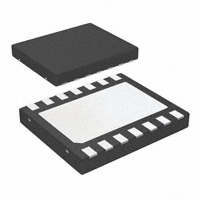


 工商网监
湘ICP备2023018690号
工商网监
湘ICP备2023018690号
