www.ti.com
Table of Contents
User’s Guide
LM2727 Buck Controller Evaluation Module User's Guide
Table of Contents
1 Introduction.............................................................................................................................................................................2
2 Boot Voltage............................................................................................................................................................................ 2
3 Dual MOSFET Footprints....................................................................................................................................................... 2
4 Low-Side Diode.......................................................................................................................................................................2
5 Additional Footprints..............................................................................................................................................................2
6 Layout Optimization............................................................................................................................................................... 3
7 PCB Layout..............................................................................................................................................................................5
8 Revision History......................................................................................................................................................................6
Trademarks
All trademarks are the property of their respective owners.
SNVA057D – AUGUST 2002 – REVISED FEBRUARY 2022
LM2727 Buck Controller Evaluation Module User's Guide
Submit Document Feedback
Copyright © 2022 Texas Instruments Incorporated
1
�Introduction
www.ti.com
1 Introduction
The LM2727 evaluation board has been designed for a wide variety of components in order to show the flexibility
of the LM2727 chips. The input voltage limitations are the same as the chip: 2.2 VDC to 16 VDC. The regulated
output voltage range is from 0.6 V up to 85% of the input voltage. Output current is limited by the components
chosen, however, the size of this board and the limitation to SOIC-8 MOSFETs means a realistic limit of about 10
A.
The example design steps 12 V down to 3.3 V at 4 A, with a switching frequency of 800 kHz. This design can be
modified by following the Design Considerations section of the LM2727/LM2737 N-Channel FET Synchronous
Buck Regulator Controller for Low Output Voltages data sheet.
The board is four layers, consisting of signal/power traces on top and bottom, with one internal ground plane and
an internal split power plane. All planes are 1-oz. copper, and the board is 62-mil FR4 laminate.
2 Boot Voltage
The default circuit that comes with the LM2727 demo board uses a bootstrap diode and small capacitor (D1 and
CBOOT) to provide enough gate-to-source voltage on the high-side MOSFET to drive the FET. If a separate rail
is available that is more than twice the value of VIN, this higher voltage can be connected directly to the BOOT
pin, through the BOOT connector, with a 0.1-µF bypass capacitor, CC. In this case, D1 and CBOOT should be
removed from the board. Do not connect both CC and CBOOT/D1 at the same time.
3 Dual MOSFET Footprints
The LM2727 demo board has two extra footprints for dual N-channel MOSFETs in SOIC-8 packages. Footprint
Q3 corresponds to devices with footprints such as the Si4816DY "LITTLEFOOT Plus" from Vishay Siliconix.
Footprint Q4 corresponds to devices with footprints such as the Si4826DY, also from Vishay Siliconix.
4 Low-Side Diode
A footprint D2 is available for a Schottky diode to be placed in parallel with the low-side FET. This can improve
efficiency because a discrete Schottky will have a lower forward voltage than the bodu diode of the low-side FET.
The footprint fits SMA size devices. If desired, the low side FET can be removed entirely, and the LM2727 will
run as an asynchronous buck controller.
5 Additional Footprints
The 1206 footprints Rc2 and Cc3 are available for designs with more complex compensation needs.
SOIC-8
Figure 5-1. Pinout for Dual FET for Footprint Q3
SOIC-8
Figure 5-2. Pinout for Dual FET for Footprint Q4
2
LM2727 Buck Controller Evaluation Module User's Guide
SNVA057D – AUGUST 2002 – REVISED FEBRUARY 2022
Submit Document Feedback
Copyright © 2022 Texas Instruments Incorporated
�www.ti.com
Layout Optimization
6 Layout Optimization
The LM2727 PCB layout could be improved with several techniques used in switching converter design. The
traces that run from the HG and LG pins of the IC to the gates of the high-side and low-side MOSFETs should be
shorter and thicker, reducing their parasitic inductance and resistance. The mid-frequency decoupling capacitor,
CINX, should be placed as close to the pins of the high-side MOSFET as possible. The bulk input capacitors,
CIN1 and CIN2, should also be placed close, keeping the loop between the input capacitors and the high-side
MOSFET small. Likewise, the Schottky diode D2 should be located as close as possible to the pins of the
low-side MOSFET. The local capacitors CIN, CBOOT, and CC (if used) should be close to the pins of the LM2727
IC. These techniques help reduce parasitic inductance throughout the PCB.
Figure 6-1. Circuit Schematic
SNVA057D – AUGUST 2002 – REVISED FEBRUARY 2022
LM2727 Buck Controller Evaluation Module User's Guide
Submit Document Feedback
Copyright © 2022 Texas Instruments Incorporated
3
�Layout Optimization
www.ti.com
Table 6-1. Bill of Materials for Typical Application Circuit
4
ID
Part Number
Type
U1
LM2727
Q1
Si4884DY
N-MOSFET
SOIC-8
Q2
Si4884DY
N-MOSFET
SOIC-8
Synchronous
Controller
Schottky Diode
Size
Parameters
Qty.
Vendor
1
NSC
13.5 mΩ, at 4.5 V, 15.3 nC
1
Vishay
13.5 mΩ, at 4.5 V, 15.3 nC
1
Vishay
TSSOP-14
Db
BAT-54
SOT-23
30 V
1
ON
Lin
P1168.162T
Inductor
12 × 12 × 4.5 mm
1.6 µH, 8.5 A, 5.4 mΩ
1
Pulse
Inductor
12 × 12 × 4.5 mm
1.6 µH, 8.5 A, 5.4 mΩ
1
Pulse
1812
10 µF, 25 V, 3.3 Arms
2
TDK
L1
P1168.162T
Cin1
C4532X5R1E106M
Capacitor
Cinx
C3216X7R1E105K
Capacitor
1206
1 µF, 25 V
1
TDK
Co1
6TPB470M
Capacitor
7.3 × 4.3 × 3.8 mm
470 µF, 2.5 V, 55 mΩ
2
Sanyo
Cin
C3216X7R1E225K
Capacitor
1206
2.2 µF, 25 V
1
TDK
Css
VJ1206X123KXX
Capacitor
1206
12 nF, 25 V
1
Vishay
Cc1
VJ1206A3R9KXX
Capacitor
1206
3.9 pF, 10%
1
Vishay
Cc2
VJ1206A391KXX
Capacitor
1206
390 pF, 10%
1
Vishay
Rin
CRCW1206100J
Resistor
1206
10 Ω, 5%
1
Vishay
Rfadj
CRCW12063052F
Resistor
1206
30.5 kΩ, 1%
1
Vishay
Rc1
CRCW12069532F
Resistor
1206
95.3 kΩ, 1%
1
Vishay
Rfb1
CRCW12064871F
Resistor
1206
4.87 kΩ, 1%
1
Vishay
Rfb2
CRCW12062181F
Resistor
1206
21.8 kΩ, 1%
1
Vishay
Rcs
CRCW1206272J
Resistor
1206
2.7 kΩ, 5%
1
Vishay
LM2727 Buck Controller Evaluation Module User's Guide
SNVA057D – AUGUST 2002 – REVISED FEBRUARY 2022
Submit Document Feedback
Copyright © 2022 Texas Instruments Incorporated
�www.ti.com
PCB Layout
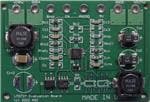
7 PCB Layout
Figure 7-1. PCB Top Layer and Top Overlay
Figure 7-2. PCB Bottom Layer and Internal Power Plane
SNVA057D – AUGUST 2002 – REVISED FEBRUARY 2022
LM2727 Buck Controller Evaluation Module User's Guide
Submit Document Feedback
Copyright © 2022 Texas Instruments Incorporated
5
�Revision History
www.ti.com
Figure 7-3. PCB Overall
8 Revision History
NOTE: Page numbers for previous revisions may differ from page numbers in the current version.
Changes from Revision C (April 2013) to Revision D (February 2022)
Page
• Updated the numbering format for tables, figures, and cross-references throughout the document. ................2
• Updated the user's guide title............................................................................................................................. 2
6
LM2727 Buck Controller Evaluation Module User's Guide
SNVA057D – AUGUST 2002 – REVISED FEBRUARY 2022
Submit Document Feedback
Copyright © 2022 Texas Instruments Incorporated
�IMPORTANT NOTICE AND DISCLAIMER
TI PROVIDES TECHNICAL AND RELIABILITY DATA (INCLUDING DATA SHEETS), DESIGN RESOURCES (INCLUDING REFERENCE
DESIGNS), APPLICATION OR OTHER DESIGN ADVICE, WEB TOOLS, SAFETY INFORMATION, AND OTHER RESOURCES “AS IS”
AND WITH ALL FAULTS, AND DISCLAIMS ALL WARRANTIES, EXPRESS AND IMPLIED, INCLUDING WITHOUT LIMITATION ANY
IMPLIED WARRANTIES OF MERCHANTABILITY, FITNESS FOR A PARTICULAR PURPOSE OR NON-INFRINGEMENT OF THIRD
PARTY INTELLECTUAL PROPERTY RIGHTS.
These resources are intended for skilled developers designing with TI products. You are solely responsible for (1) selecting the appropriate
TI products for your application, (2) designing, validating and testing your application, and (3) ensuring your application meets applicable
standards, and any other safety, security, regulatory or other requirements.
These resources are subject to change without notice. TI grants you permission to use these resources only for development of an
application that uses the TI products described in the resource. Other reproduction and display of these resources is prohibited. No license
is granted to any other TI intellectual property right or to any third party intellectual property right. TI disclaims responsibility for, and you
will fully indemnify TI and its representatives against, any claims, damages, costs, losses, and liabilities arising out of your use of these
resources.
TI’s products are provided subject to TI’s Terms of Sale or other applicable terms available either on ti.com or provided in conjunction with
such TI products. TI’s provision of these resources does not expand or otherwise alter TI’s applicable warranties or warranty disclaimers for
TI products.
TI objects to and rejects any additional or different terms you may have proposed. IMPORTANT NOTICE
Mailing Address: Texas Instruments, Post Office Box 655303, Dallas, Texas 75265
Copyright © 2022, Texas Instruments Incorporated
�