www.ti.com
Table of Contents
User’s Guide
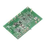
LM2744 Buck Controller Evaluation Module User's Guide
Table of Contents
1 Introduction.............................................................................................................................................................................2
2 Additional Footprints..............................................................................................................................................................3
3 Guidelines for Additional Options.........................................................................................................................................4
4 Typical Application Circuit.....................................................................................................................................................5
5 Performance Characteristics.................................................................................................................................................6
5.1 Load Transient Response.................................................................................................................................................. 6
5.2 Switch Node Voltage and Output Ripple Voltage............................................................................................................... 6
6 PCB Layout Diagrams............................................................................................................................................................ 8
7 Revision History......................................................................................................................................................................8
Trademarks
All trademarks are the property of their respective owners.
SNVA103B – OCTOBER 2005 – REVISED FEBRUARY 2022
LM2744 Buck Controller Evaluation Module User's Guide
Submit Document Feedback
Copyright © 2022 Texas Instruments Incorporated
1
�Introduction
www.ti.com
1 Introduction
This user's guide describes the LM2743 printed circuit board (PCB) design and provides an example typical
application circuit. The demo board allows component design flexibility in order to demonstrate the versatility of
the LM2744 IC.
The demo board contains a voltage-mode, high-speed synchronous buck regulator controller with an external
adjustable reference voltage between 0.5 V and 1.5 V. The demo board design incorporates the LM4140 high
precision low noise reference IC providing 1.0 V to the reference pin (VREF). Though the control sections of the
IC are rated for 3 to 6 V (VCC), the driver sections are designed to accept input supply rails (VIN) as high as 14 V.
It operates at a fixed frequency, adjustable from 50 kHz to 1 MHz with one external resistor.
The demo board design regulates to an output voltage of 1.2 V at 3.5 A with a switching frequency of 1 MHz.
Note, the demo board is optimized for a 1-MHz, 14-V input voltage compensation design. If another switching
frequency and input voltage is desired, please consult the LM2744 Low Voltage N-Chan MOSFET Synch Buck
Regr Cntrl w/ Ext Ref data sheet for control loop compensation procedures. For additional design modifications,
refer to the Design Consideration section of the LM2744 Low Voltage N-Chan MOSFET Synch Buck Regr Cntrl
w/ Ext Ref data sheet.
2
LM2744 Buck Controller Evaluation Module User's Guide
SNVA103B – OCTOBER 2005 – REVISED FEBRUARY 2022
Submit Document Feedback
Copyright © 2022 Texas Instruments Incorporated
�www.ti.com
Additional Footprints
2 Additional Footprints
A Schottky diode footprint (D1) is available in parallel to the low-side MOSFET. This component can improve
efficiency, due to the lower forward drop than the low-side MOSFET body diode conducting during the antishoot–through period. Select a Schottky diode that maintains a forward drop around 0.4 V to 0.6 V at the
maximum load current (consult the I-V curve). In addition, select the reverse breakdown voltage to have
sufficient margin above the maximum input voltage.
Footprint C13 is available for a multilayer ceramic capacitor (MLCC) connected as close as possible to the
source of the low-side MOSFET and drain of the high-side MOSFET. This will provide low supply impedance
to the high speed switch currents, thus minimizing the input supply noise. For example; a MLCC is used (C13)
in combination with aluminum electrolytic input filter capacitors, placed in designators C12 and C14, because
MLCC has lower impedance than electrolytics. If MLCCs are used in designators C12 and C14, component C13
is not necessary.
The PCB is designed on two layers with 1-oz. copper on a 62-mil FR4 laminate.
SNVA103B – OCTOBER 2005 – REVISED FEBRUARY 2022
LM2744 Buck Controller Evaluation Module User's Guide
Submit Document Feedback
Copyright © 2022 Texas Instruments Incorporated
3
�Guidelines for Additional Options
www.ti.com
3 Guidelines for Additional Options
When using a DC power supply to set a reference voltage (VREF), connect a capacitor (C20) from VDCS to GND
to filter the DC power supply. A good starting point is 10 µF, but it may need to be varied depending on the
magnitude of the DC power supply noise (any make of capacitor will do as long as the capacitance is maintained
within the operating temperature range). Remove R10 and place a 0-Ω jumper in designator R12.
Designators R12 and R13 are provided for DDR SDRAM (double data rate synchronous dynamic random
access memory) active termination design. Set VREF to half the DDR supply voltage by using designators R12
and R13 as a voltage divider. Remove resistors R7 and R10 and capacitor C21, and connect the DDR supply
voltage rail to terminal VDCS. Refer to Figure 4-2. The modified circuit in Figure 4-1 can sink or source current in
excess of 3 A. A load transient response applied to the output of Figure 4-2 is provided in Figure 5-1.
Do not exceed 5.6 V on the VCC pin of the demo board. The board layout connects both the input voltage of
the LM4140-1.0 (pin 2) and the control section of the LM2744 (VCC). The maximum DC supply voltage for the
control section of the LM2744 is 6 V, while 5.6 V is the maximum rating for any input pin of the LM4140. If the
design requires the control section of the LM2744 to be 6 V, a shunt zener reference can be placed at designator
location (D3) to maintain the input voltage of the LM4140 between 1.8 V and 5.5 V. The cathode of the zener is
connected to the input of the LM4140 and the anode to GND. The resistance of R10 must be selected to supply
the appropriate amount of biasing current into the zener and the LM4140 (refer to the Electrical Characteristics
table of the LM2744 Low Voltage N-Chan MOSFET Synch Buck Regr Cntrl w/ Ext Ref data sheet.
4
LM2744 Buck Controller Evaluation Module User's Guide
SNVA103B – OCTOBER 2005 – REVISED FEBRUARY 2022
Submit Document Feedback
Copyright © 2022 Texas Instruments Incorporated
�www.ti.com
Typical Application Circuit
4 Typical Application Circuit
The typical application circuit in Figure 4-1 provides the component designators used on the demo board.
VC
D2
C
VIN
C10
R11
R1
C12
VCC
J1
C5
HG
SD
BOOT
PWGD
FREQ
R10
R2
C7
C22
EN
Q1
VOUT
L1
R4
ISEN
LM2744
LG
SS/TRACK
SGND
VREF
PGND
+
Q2
C16
FB
EAO
VEN
C14
R8
C9
VREF
R5
LM4140
-1.0
C11
R6
C8
R3
C21
R7
PGND
NC
Figure 4-1. Typical Application
VC
D2
C
C12
VCC
J1
C5
HG
BOO
T
ISEN
SD
PWGD
FREQ
R2
C7
R12
VDCS
+
C20
VIN
R11
R8
R1
C10
LM2744
C14
Q1
VOUT
L1
R4
LG
SS/TRACK
SGND
VREF
PGND
+
Q2
C16
FB
EAO
C21/
R13
C9
R5
R3
C11
R6
C8
Figure 4-2. DDR SDRAM Termination Supply
SNVA103B – OCTOBER 2005 – REVISED FEBRUARY 2022
LM2744 Buck Controller Evaluation Module User's Guide
Submit Document Feedback
Copyright © 2022 Texas Instruments Incorporated
5
�Performance Characteristics
www.ti.com
5 Performance Characteristics
5.1 Load Transient Response
Figure 5-1. ±3-A Load Transient Response Applied
to the Circuit in Figure 4-2 (VIN = VCC = 3.3 V and
VOUT = 1.2 V). CH 2 - VOUT AC Coupled and CH 3 - 5
A/DIV
Figure 5-2. Efficiency vs. Load Current VOUT = 1.2
V, fSW = 1 MHz
5.2 Switch Node Voltage and Output Ripple Voltage
Figure 5-3. VIN = VCC = 3.3 V, VOUT = 1.2 V, ILOAD = 0
A, fSW = 1 MHz, 20-MHz Bandwidth Limit
Figure 5-4. VIN = VCC = 3.3 V, VOUT = 1.2 V, ILOAD =
3.5 A, fSW = 1 MHz, 20-MHz Bandwidth Limit
Figure 5-5. VIN = 14 V, VCC = 5 V, VOUT = 1.2 V, ILOAD
= 0 A, fSW = 1 MHz, 20-MHz Bandwidth Limit
Figure 5-6. VIN = 14 V, VCC = 5 V, VOUT = 1.2 V, ILOAD
= 3.5 A, fSW = 1 MHz, 20-MHz Bandwidth Limit
Table 5-1. Bill of Materials
Designator
6
Function
Part Description
Part Number
U1
Controller
IC LM2744 TSSOP14
Texas Instruments
U2
Low Dropout Reg
IC LM4140BCM-1.0 SOIC-8
Texas Instruments
C5
VCC Decoupling
Ceramic Capacitor, 1 µF, 25 V, 10%, 0805
Murata GRM216R61E105KA12B
C7
Soft Start Cap
Ceramic Capacitor, 12 nF, 25 V, 10%, 0805
Vishay VJ0805Y123KXX
LM2744 Buck Controller Evaluation Module User's Guide
SNVA103B – OCTOBER 2005 – REVISED FEBRUARY 2022
Submit Document Feedback
Copyright © 2022 Texas Instruments Incorporated
�www.ti.com
Performance Characteristics
Table 5-1. Bill of Materials (continued)
Designator
Function
Part Description
Part Number
C8
Comp Cap
Ceramic Capacitor, 1.2 nF, 25 V, 10%, 0805
Vishay VJ0805Y122KXX
C9
Comp Cap
Ceramic Capacitor, 15 pF, 50 V, 10%, 0805
Vishay VJ0805A150KAA
C10
Cboot
Ceramic Capacitor, 0.1 µF, 25 V, 10%, 0805
Vishay VJ0805Y104KXX
C11
Comp Cap
Ceramic Capacitor, 1.8 nF, 25 V, 10%, 0805
Vishay VJ0805Y182KXX
C12
Input Filter Cap
Ceramic Capacitor, 10 μF, 25 V, 10%, 1210
AVX 12103D106MAT
C14
Input Filter Cap
Ceramic Capacitor, 10 μF, 25 V, 10%, 1210
AVX 12103D106MAT
C16
Output Filter Cap
470 μF, 6.3 V, 10-mΩ ESR POScap
Sanyo 6TPD470
C21
Reference Output Cap
Niobium Oxide Capacitor, 4.7 µF, 6 V
AVX NOJA475M0006R
C22
Reference Input Cap
Ceramic Capacitor, 0.47 µF, 25 V, 10%, 1206
Vishay VJ1206Y474KXX
R1
VCC Filter Resistor
Resistor 10 Ω, .25 W, 0805
Vishay CRCW08051000F
R2
Frequency Adjust Resistor
Resistor, 24.9 kΩ, .25 W, 0805
Vishay CRCW08052492F
R3
Comp Resistor
Resistor, 21 kΩ, .25 W, 0805
Vishay CRCW08052102F
R4
Current Limit Resistor
Resistor, 3.16 kΩ, .25 W, 0805
Vishay CRCW08053161F
R5
Comp Resistor
Resistor, 2.94 kΩ, .25 W, 0805
Vishay CRCW08052941F
R6
Resistor Divider, upper
Resistor, 10.0 kΩ, .25 W, 0805
Vishay CRCW08051002F
R7
Resistor Divider, lower
Resistor, 59 kΩ, .25 W, 0805
Vishay CRCW08055902F
R8
PWGD Pull-Up
Resistor, 100 kΩ, .25 W, 0805
Vishay CRCW08051003F
R10
Zero Ohm
Resistor, 0 Ω, 0805
Vishay CRCW08050000
R11
Shut Down Pull-Up
Resistor, 100 kΩ, .25 W, 0805
Vishay CRCW12061003F
D2
Bootstrap Diode
Schottky Diode, SOD-123
MBR0530LTI
L1
Output Filter Inductor
Inductor 1 µH, 5.3 Arms, 10.2 mΩ
Cooper DR73-1R0
Q1-Q2
Top and Bottom FETs
Dual N-MOSFET, VDS = 20 V, 24 mΩ at 2.5 V
Vishay 9926BDY
V
CC
V
D2
R 11
R8
C 13
C 12
C 14
V CC
HG
J1
C5
IN
C 10
SD
BO O T
IS E N
Q 1
V
L1
R4
O UT
PW G D
FR EQ
LM 2744
LG
R2
R 10
V
C7
REF
S S /T R A C K
SG N D
VR EF
PG N D
D3
C 22
EN
REF
LM 4140
-1 .0
PG N D
C 15
+
+
C 16
C9
R9
V
D1
FB
EAO
V IN
Q 2
R5
R3
C 11
R6
C8
C 21
R7
NC
Figure 5-7. Complete Demo Board Schematic
SNVA103B – OCTOBER 2005 – REVISED FEBRUARY 2022
LM2744 Buck Controller Evaluation Module User's Guide
Submit Document Feedback
Copyright © 2022 Texas Instruments Incorporated
7
�PCB Layout Diagrams
www.ti.com
6 PCB Layout Diagrams
Figure 6-1. Top Layer and Top Overlay
Figure 6-2. Bottom Layer
7 Revision History
NOTE: Page numbers for previous revisions may differ from page numbers in the current version.
Changes from Revision A (April 2013) to Revision B (February 2022)
8
LM2744 Buck Controller Evaluation Module User's Guide
Page
SNVA103B – OCTOBER 2005 – REVISED FEBRUARY 2022
Submit Document Feedback
Copyright © 2022 Texas Instruments Incorporated
�IMPORTANT NOTICE AND DISCLAIMER
TI PROVIDES TECHNICAL AND RELIABILITY DATA (INCLUDING DATA SHEETS), DESIGN RESOURCES (INCLUDING REFERENCE
DESIGNS), APPLICATION OR OTHER DESIGN ADVICE, WEB TOOLS, SAFETY INFORMATION, AND OTHER RESOURCES “AS IS”
AND WITH ALL FAULTS, AND DISCLAIMS ALL WARRANTIES, EXPRESS AND IMPLIED, INCLUDING WITHOUT LIMITATION ANY
IMPLIED WARRANTIES OF MERCHANTABILITY, FITNESS FOR A PARTICULAR PURPOSE OR NON-INFRINGEMENT OF THIRD
PARTY INTELLECTUAL PROPERTY RIGHTS.
These resources are intended for skilled developers designing with TI products. You are solely responsible for (1) selecting the appropriate
TI products for your application, (2) designing, validating and testing your application, and (3) ensuring your application meets applicable
standards, and any other safety, security, regulatory or other requirements.
These resources are subject to change without notice. TI grants you permission to use these resources only for development of an
application that uses the TI products described in the resource. Other reproduction and display of these resources is prohibited. No license
is granted to any other TI intellectual property right or to any third party intellectual property right. TI disclaims responsibility for, and you
will fully indemnify TI and its representatives against, any claims, damages, costs, losses, and liabilities arising out of your use of these
resources.
TI’s products are provided subject to TI’s Terms of Sale or other applicable terms available either on ti.com or provided in conjunction with
such TI products. TI’s provision of these resources does not expand or otherwise alter TI’s applicable warranties or warranty disclaimers for
TI products.
TI objects to and rejects any additional or different terms you may have proposed. IMPORTANT NOTICE
Mailing Address: Texas Instruments, Post Office Box 655303, Dallas, Texas 75265
Copyright © 2022, Texas Instruments Incorporated
�