www.ti.com
Table of Contents
User’s Guide
LM2745 Buck Controller Evaluation Module User's Guide
Table of Contents
1 Introduction.............................................................................................................................................................................2
2 Specifics Of The Board.......................................................................................................................................................... 2
3 Feature Options...................................................................................................................................................................... 2
4 Specification Summary.......................................................................................................................................................... 3
5 Performance Characteristics – Efficiency............................................................................................................................3
6 Switch Node Voltage and Output Voltage Ripple.................................................................................................................4
7 Load Transient Response...................................................................................................................................................... 5
8 Bill of Materials....................................................................................................................................................................... 6
9 PCB Layout..............................................................................................................................................................................8
10 Revision History................................................................................................................................................................... 9
Trademarks
All trademarks are the property of their respective owners.
SNVA213B – MAY 2007 – REVISED FEBRUARY 2022
Submit Document Feedback
LM2745 Buck Controller Evaluation Module User's Guide
Copyright © 2022 Texas Instruments Incorporated
1
�Introduction
www.ti.com
1 Introduction
This user's guide describes the LM2745 printed circuit board (PCB) design and provides an example typical
application circuit. The LM2745 is a voltage mode PWM buck controller that implements synchronous
rectification. It provides a low-cost, high power density, and efficient point of load solution. In steady state
operation, the LM2745 is always synchronous, even at no load, simplifying the compensation design. The
LM2745 ensures a smooth and controlled start-up when the output is pre-biased. The current limit protection
does not require a current limit resistor in the power path, but is achieved by sensing the voltage VDS across the
low side MOSFET. Though the control sections of the IC are rated for 3 V to 6 V (VCC), the driver sections are
designed to accept input supply rails (VIN) as high as 14 V.
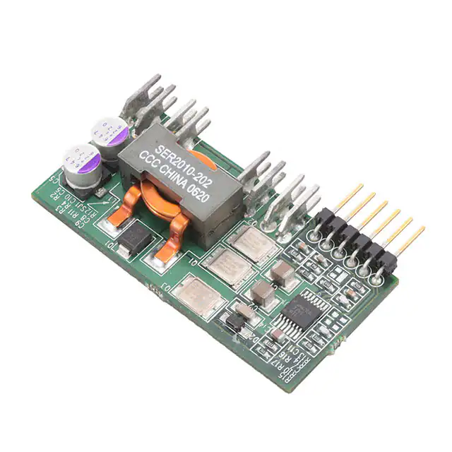
2 Specifics Of The Board
This demo board targets the fixed and mobile telecommunications, industrial electronics, and distributed power
markets. The demo board has a VIN range of 8 V to 14 V and a LDO regulator, the LP2937, powers VCC by
regulating a 5-V output voltage. The LM2745 regulates to an output range of 1.2 V to 3.3 V at 19 A with a
switching frequency of 300 kHz. The demo board is optimized for the previously mentioned parameters, thus
for additional design modifications, refer to the Design Consideration section of the LM2745/48 Synch Buck
Controller w/ Pre-Bias Startup & Optional Clock Synchronization data sheet. The PCB is designed on four layers.
The top and bottom layers are 2-oz. copper and the two inner layers are 1-oz. copper. The board measures 2.19
inch × 1.03 inch × 0.41 inch (56 mm × 26.2 mm × 10.3 mm) (l × w × h) on a FR4 laminate.
3 Feature Options
When the tracking feature of the LM2745 is required for use, remove the jumper that connects the soft-start
capacitor, C10, and connect the resistor divider, on designators R13 and R14 (see Figure 3-1). The Track
terminal has been provided for the user's connecting convenience. The demo board is synchronize ready, just
connect an external clock to the SYNC terminal.
Note
Increasing the switching frequency results in a lower inductor current ripple and input and output
voltage ripple (if the component values are kept the same).
Monitor the MOSFET junction temperature since switching losses will increase, and do not exceed the maximum
junction temperature of the MOSFET. Refer to the MOSFET manufacturer data sheet for the maximum junction
temperature specification and heat sinking guidelines.
Connects SoftStart Capacitor
SJ1
SJ1
Connects Tracking
Resistors
Figure 3-1. Soft-Start and Tracking Jumper
2
LM2745 Buck Controller Evaluation Module User's Guide
Copyright © 2022 Texas Instruments Incorporated
SNVA213B – MAY 2007 – REVISED FEBRUARY 2022
Submit Document Feedback
�www.ti.com
Specification Summary
4 Specification Summary
•
•
•
•
•
•
•
•
•
•
•
•
•
•
Space saving footprint
Wide ambient temperature range: –40°C to 65°C
Input voltage range: 8 V to 14 V
Adjustable output voltage: 1.2 V to 3.3 V
No minimum load requirement
Remote ON/OFF
Power-good signal
Fixed switching frequency: 300 kHz
Switching frequency synchronize range 250 kHz to 1 MHz
Current limit protection
Controller power supply start-up tracking function
Start-up with a pre-biased output load
Adjustable soft start
Small size: 2.19 inch × 1.03 inch × 0.41 inch (56 mm × 26.2 mm × 10.3 mm)
5 Performance Characteristics – Efficiency
Figure 5-1. Efficiency vs. Load Current VOUT = 3.3 V, fSW = 300 kHz
SNVA213B – MAY 2007 – REVISED FEBRUARY 2022
Submit Document Feedback
LM2745 Buck Controller Evaluation Module User's Guide
Copyright © 2022 Texas Instruments Incorporated
3
�Switch Node Voltage and Output Voltage Ripple
www.ti.com
6 Switch Node Voltage and Output Voltage Ripple
4
Figure 6-1. VIN = 8 V, VOUT = 3.3 V, ILOAD = 100 mA,
fSW = 300 kHz, 20-MHz Bandwidth Limit
Figure 6-2. VIN = 8 V, VOUT = 3.3 V, ILOAD = 19 A, fSW
= 300 kHz, 20-MHz Bandwidth Limit
Figure 6-3. VIN = 14 V, VOUT = 3.3 V, ILOAD = 100 mA,
fSW = 300 kHz, 20-MHz Bandwidth Limit
Figure 6-4. VIN = 14 V, VOUT = 3.3 V, ILOAD = 19 A,
fSW = 300 kHz, 20-MHz Bandwidth Limit
LM2745 Buck Controller Evaluation Module User's Guide
Copyright © 2022 Texas Instruments Incorporated
SNVA213B – MAY 2007 – REVISED FEBRUARY 2022
Submit Document Feedback
�www.ti.com
Load Transient Response
7 Load Transient Response
5A/DIV
2A/DIV
50 mV/DIV
50 mV/DIV
100 µs/DIV
100 µs/DIV
Figure 7-1. VIN = 14 V, VOUT = 3.3 V ILOAD = 2A to
10A, CH1: VOUT, CH2: ILOAD
Figure 7-2. VIN = 14 V, VOUT = 3.3 V, ILOAD = 11 A to
19 A, CH1: VOUT, CH2: ILOAD
5A/DIV
2A/DIV
100 mV/DIV
100 mV/DIV
100 µs/DIV
100 µs/DIV
Figure 7-3. VIN = 8 V, VOUT = 3.3 V, ILOAD = 2 A to 10 Figure 7-4. VIN = 8 V, VOUT = 3.3 V, ILOAD = 11 A to 19
A, CH1: VOUT, CH2: ILOAD
A, CH1: VOUT, CH2: ILOAD
SNVA213B – MAY 2007 – REVISED FEBRUARY 2022
Submit Document Feedback
LM2745 Buck Controller Evaluation Module User's Guide
Copyright © 2022 Texas Instruments Incorporated
5
�Bill of Materials
www.ti.com
8 Bill of Materials
Table 8-1. Bill of Materials for LM2745 POL EVB (VIN: 8 V to 14 V, VOUT: 3.3 V, 19 A)
Location
6
Part Number
Type
Size
Parameters
Qty
Vendor
U1
LM2745
Syn. Buck Controller
TSSOP-14
VIN: 4.5 V–5.5 V
1
NSC
U2
LM27937IMP-5.0
Linear Regulator 5 V,500 mA
SOT-223
5 V, 500 mA
1
NSC
L1
SER2010-202ML
Inductor
2 μH, 27 A, 0.852 mΩ
1
Coilcraft
Q1-2
IRF6633
N-MOSFET
DirectFET-MP
20 V, 16 A, 4.1 mΩ, 11 nC
2
Vishay
Q3
IRF6609
N-MOSFET
DirectFET-MT
20 V, 150 A, 2 mΩ, 46 nC
1
Vishay
D1
SL22-E3/2C
Schottky Diode
SMB
20 V, 2 A
1
Vishay
D2
MBRS0520
Schottky Diode
SOD123
20 V, 0.5 A
1
Vishay
C1, 2
GRM32ER61C226KE20L
Ceramic Capacitor
1210
22 µF, 25 V, X7R, 5%
2
Murata
C3, 11
GRM319R71H104KA01B
Ceramic Capacitor
1206
100 nF, 25 V, X7R, 10%
2
Murata
C14
GRM319R71H474KA01B
Ceramic Capacitor
1206
470 nF, 25 V, X7R, 10%
1
Murata
C9
GRM1885C1H1210JA01
Ceramic Capacitor
0603
120 pF, 50 V, C0G, 5%
1
Murata
C6
GRM188R71H222KA01
Ceramic Capacitor
0603
2.2 nF, 50 V, X7R, 10%
1
Murata
C7
GRM1885C1H101JA01
Ceramic Capacitor
0603
100 pF, 50 V, C0G, 5%
1
Murata
C8
GRM188R71H332KA01
Ceramic Capacitor
0603
3.3 nF, 50 V, X7R, 10%
1
Murata
C10
GRM188R71H153KA01
Ceramic Capacitor
0603
15 nF, 50 V, X7R, 10%
1
Murata
C12
GRM40X7R472K25
Ceramic Capacitor
0805
470 nF, 25 V, X7R, 10%
1
Murata
C13
12066D226MAT
Ceramic Capacitor
1206
22 µF, 6.3 V, X5R, 20%
1
AVX
C4, 5
6SVPC220M
OS-CON
C6
220 µF, 6.3 V, 20%
2
Sanyo
R1,18
CRCW06030R00F
Chip Resistor
0603
0Ω
2
Vishay
R2
CRCW06032151F
Chip Resistor
0603
2.15 k, 1%
1
Vishay
R3, R17
CRCW06031002F
Chip Resistor
0603
10 k, 1%
2
Vishay
R4
CRCW06032211F
Chip Resistor
0603
2.21 k, 1%
1
Vishay
R10, 11
CRCW06031003F
Chip Resistor
0603
100 k, 1%
2
Vishay
R5, 6, 8
CRCW06032R21F
Chip Resistor
0603
2.21 Ω, 1%
3
Vishay
R7, 9
CRCW06034702F
Chip Resistor
0603
47 k, 1%
2
Vishay
R12
CRCW06038451F
Chip Resistor
0603
8.45 k, 1%
1
Vishay
R15
CRCW06031821F
Chip Resistor
0603
1.82 k, 1%
1
Vishay
R16
CRCW060310R0F
Chip Resistor
0603
10 Ω, 1%
1
Vishay
—
—
F-Pin
—
—
Pin 90 deg., SIP, 6 way
8
Pitch: 2.54 mm
LM2745 Buck Controller Evaluation Module User's Guide
1
SNVA213B – MAY 2007 – REVISED FEBRUARY 2022
Submit Document Feedback
Copyright © 2022 Texas Instruments Incorporated
�www.ti.com
Bill of Materials
SJ2
U2
LM2937
VOUT
C13
R18
VIN
C12
GND
R16
C11
D2
VIN
C14
R6
R17
R11
C2
U1
C1
R5
BOO
T
SD
SD
PWGD
Q1
HG
VCC
LM2745
PWGD
Q2
R7
VOUT
L1
R15
ISEN
C7
SYNC
FREQ/SYNC
LG
R8
Q3
R10
PGND
SS/TRACK
D1
+
C5
+
+
C4
C3
R9
SGND
PGND
EAO
R13
FB
TRACK
R14
C9
SJ1
C6
R2
R3
C8
R12
C10
TRIM
R4
SENSE
Figure 8-1. 300 kHz Demo Board Schematic
SNVA213B – MAY 2007 – REVISED FEBRUARY 2022
Submit Document Feedback
LM2745 Buck Controller Evaluation Module User's Guide
Copyright © 2022 Texas Instruments Incorporated
7
�PCB Layout
www.ti.com
9 PCB Layout
Figure 9-1. Top Silkscreen
Figure 9-2. Top Copper Layer
Figure 9-3. Bottom Silkscreen
8
LM2745 Buck Controller Evaluation Module User's Guide
Copyright © 2022 Texas Instruments Incorporated
SNVA213B – MAY 2007 – REVISED FEBRUARY 2022
Submit Document Feedback
�www.ti.com
Revision History
Figure 9-4. Bottom Copper Layer
Figure 9-5. Internal Layer-1 (GND Copper)
Figure 9-6. Internal Layer-2 (GND Copper)
10 Revision History
NOTE: Page numbers for previous revisions may differ from page numbers in the current version.
Changes from Revision A (May 2013) to Revision B (February 2022)
Page
• Updated the numbering format for tables, figures, and cross-references throughout the document. ................2
• Updated the user's guide title............................................................................................................................. 2
SNVA213B – MAY 2007 – REVISED FEBRUARY 2022
Submit Document Feedback
LM2745 Buck Controller Evaluation Module User's Guide
Copyright © 2022 Texas Instruments Incorporated
9
�IMPORTANT NOTICE AND DISCLAIMER
TI PROVIDES TECHNICAL AND RELIABILITY DATA (INCLUDING DATA SHEETS), DESIGN RESOURCES (INCLUDING REFERENCE
DESIGNS), APPLICATION OR OTHER DESIGN ADVICE, WEB TOOLS, SAFETY INFORMATION, AND OTHER RESOURCES “AS IS”
AND WITH ALL FAULTS, AND DISCLAIMS ALL WARRANTIES, EXPRESS AND IMPLIED, INCLUDING WITHOUT LIMITATION ANY
IMPLIED WARRANTIES OF MERCHANTABILITY, FITNESS FOR A PARTICULAR PURPOSE OR NON-INFRINGEMENT OF THIRD
PARTY INTELLECTUAL PROPERTY RIGHTS.
These resources are intended for skilled developers designing with TI products. You are solely responsible for (1) selecting the appropriate
TI products for your application, (2) designing, validating and testing your application, and (3) ensuring your application meets applicable
standards, and any other safety, security, regulatory or other requirements.
These resources are subject to change without notice. TI grants you permission to use these resources only for development of an
application that uses the TI products described in the resource. Other reproduction and display of these resources is prohibited. No license
is granted to any other TI intellectual property right or to any third party intellectual property right. TI disclaims responsibility for, and you
will fully indemnify TI and its representatives against, any claims, damages, costs, losses, and liabilities arising out of your use of these
resources.
TI’s products are provided subject to TI’s Terms of Sale or other applicable terms available either on ti.com or provided in conjunction with
such TI products. TI’s provision of these resources does not expand or otherwise alter TI’s applicable warranties or warranty disclaimers for
TI products.
TI objects to and rejects any additional or different terms you may have proposed. IMPORTANT NOTICE
Mailing Address: Texas Instruments, Post Office Box 655303, Dallas, Texas 75265
Copyright © 2022, Texas Instruments Incorporated
�