Product
Folder
Sample &
Buy
Support &
Community
Tools &
Software
Technical
Documents
LM2753
SNVS353F – FEBRUARY 2005 – REVISED SEPTEMBER 2016
LM2753 High-Power Switched-Capacitor Voltage Converter and Flash LED Driver
1 Features
3 Description
•
•
•
•
The LM2753 is capable of driving a flash LED with a
pulsed current of 400 mA at an input voltage of 3.6 V.
A switched-capacitor doubler, the LM2753 provides a
regulated 5-V output (VOUT) over an input supply
range of 3 V to 5.5 V. The switched output, IOUT,
takes less than 10 ns to turn on and provide
maximum current to a flash LED. Flash LED current
is set via a ballast resistor. Continuous illumination
current (torch mode) is programmed by connecting a
resistor between IOUT and VOUT. This device uses
only three small, low-cost ceramic capacitors.
1
•
•
•
•
•
Input Voltage Range: 3 V to 5.5 V
Regulated 5-V Output
250-mA Output Current With a 3.6-V Input
400-mA Pulsed Output Current
(up to 500-ms Duration)
60-µA (Typical) Quiescent Current
Pulse-Frequency Modulation (PFM) Regulation
Inductor-Less Solution: Requires Only Three
Small Capacitors
< 1-µA Typical Shutdown Current
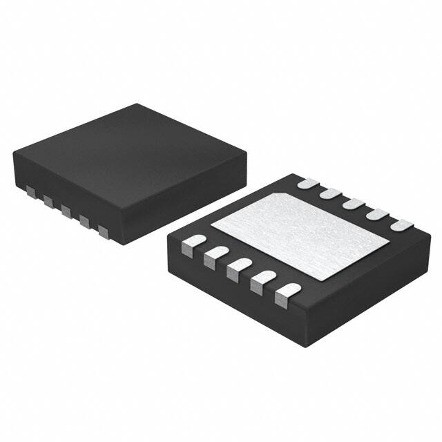
10-pin WSON Package (No Pullback):
– 3 mm × 3 mm × 0.8 mm
The LM2753 device uses pulse frequency modulation
(PFM) regulation. Typical operating frequency is
725 kHz. Under no-load conditions, the LM2753
operates on only 60 µA. If the output is connected to
ground, the charge pump stays in the gain of 1, which
helps limit the input current to 300 mA (typical).
2 Applications
•
•
•
•
•
•
•
•
Cell-Phone Camera Flash
Digital Still Cameras
Fire-Alarm Notification
Emergency Strobe Lighting
Intruder Alert Notification
Barcode Scanners
Handheld Data Terminals
General-Purpose Regulated Voltage Output, HighCurrent Supply
Device Information(1)
PART NUMBER
LM2753
PACKAGE
BODY SIZE (NOM)
WSON (10)
3.00 mm × 3.00 mm
(1) For all available packages, see the orderable addendum at
the end of the data sheet.
Simplified Schematic
VIN = 3 V - 5.5 V
2
CIN
1
VOUT = 5 V
VIN
VOUT
9
C1+
RTORCH
COUT
C1
3
TORCH
FLASH
(Need TORCH
³21´ WR )/$6+)
6
LM2753
C1-
IOUT
EN
GND
4
8 RFLASH
FLASH
10
7
5
Flash
LED
Copyright © 2016, Texas Instruments Incorporated
1
An IMPORTANT NOTICE at the end of this data sheet addresses availability, warranty, changes, use in safety-critical applications,
intellectual property matters and other important disclaimers. PRODUCTION DATA.
�LM2753
SNVS353F – FEBRUARY 2005 – REVISED SEPTEMBER 2016
www.ti.com
Table of Contents
1
2
3
4
5
6
7
Features ..................................................................
Applications ...........................................................
Description .............................................................
Revision History.....................................................
Pin Configuration and Functions .........................
Specifications.........................................................
1
1
1
2
3
4
6.1
6.2
6.3
6.4
6.5
6.6
4
4
4
4
5
5
Absolute Maximum Ratings ......................................
ESD Ratings..............................................................
Recommended Operating Conditions.......................
Thermal Information ..................................................
Electrical Characteristics...........................................
Typical Characteristics ..............................................
Detailed Description .............................................. 6
7.1
7.2
7.3
7.4
Overview ...................................................................
Functional Block Diagram .........................................
Feature Description...................................................
Device Functional Modes..........................................
6
6
6
9
8
Application and Implementation ........................ 10
8.1 Application Information............................................ 10
8.2 Typical Application ................................................. 10
9 Power Supply Recommendations...................... 13
10 Layout................................................................... 13
10.1 Layout Guidelines ................................................. 13
10.2 Layout Example .................................................... 13
11 Device and Documentation Support ................. 14
11.1
11.2
11.3
11.4
11.5
11.6
11.7
Device Support......................................................
Documentation Support .......................................
Receiving Notification of Documentation Updates
Community Resources..........................................
Trademarks ...........................................................
Electrostatic Discharge Caution ............................
Glossary ................................................................
14
14
14
14
14
14
14
12 Mechanical, Packaging, and Orderable
Information ........................................................... 14
4 Revision History
NOTE: Page numbers for previous revisions may differ from page numbers in the current version.
Changes from Revision E (July 2016) to Revision F
•
Page
Added several Applications ................................................................................................................................................... 1
Changes from Revision D (May 2013) to Revision E
Page
•
Added Device Information and Pin Configuration and Functions sections, ESD Ratings, Feature Description, Device
Functional Modes, Application and Implementation, Power Supply Recommendations, Layout, Device and
Documentation Support, and Mechanical, Packaging, and Orderable Information sections ................................................. 1
•
Changed RθJA from "55°C/W" to "52.5°C/W"; add additional thermal values ........................................................................ 4
Changes from Revision C (April 2013) to Revision D
•
2
Page
Changed layout of National Semiconductor data Sheet to TI format ................................................................................... 11
Submit Documentation Feedback
Copyright © 2005–2016, Texas Instruments Incorporated
Product Folder Links: LM2753
�LM2753
www.ti.com
SNVS353F – FEBRUARY 2005 – REVISED SEPTEMBER 2016
5 Pin Configuration and Functions
DSC Package
10-Pin WSON
Top View
C1+
1
10
GND
VIN
2
9
VOUT
C1-
3
8
IOUT
FLASH
4
7
GND
GND
5
6
EN
Die-Attach Pad:
GND
Pin Descriptions
PIN
NUMBER
NAME
1
C1+
2
3
TYPE
DESCRIPTION
O
Flying capacitor connection
VIN
I
Input voltage connection. Input voltage range: 3 V to 5.5 V
C1–
O
Flying capacitor connection
4
FLASH
I
Flash logic input pin. Logic HIGH = flash output on, logic low = flash output off. there is
an internal pulldown of 300 kΩ between FLASH and GND.
5
GND
—
6
EN
I
7
GND
—
Connect to ground
8
IOUT
O
Flash output. ON/OFF control via FLASH pin
9
VOUT
O
5-V regulated output
10
GND
—
Connect to ground
Connect to ground
Enable pin. Logic HIGH = enable, Logic LOW = shutdown. There is an internal pulldown
of 300 kΩ between EN and GND
Submit Documentation Feedback
Copyright © 2005–2016, Texas Instruments Incorporated
Product Folder Links: LM2753
3
�LM2753
SNVS353F – FEBRUARY 2005 – REVISED SEPTEMBER 2016
www.ti.com
6 Specifications
6.1 Absolute Maximum Ratings
over operating free-air temperature range (unless otherwise noted) (1) (2)
MIN
MAX
UNIT
VIN pin: voltage to GND
–0.3
6
V
EN, FLASH pins: voltage to GND
–0.3
(VIN + 0.3) w/ 6 V maximum
V
Continuous power dissipation (3)
Internally limited
Junction temperature, TJ-MAX-ABS
−65
Storage temperature, Tstg
(1)
(2)
(3)
150
°C
150
°C
Stresses beyond those listed under Absolute Maximum Ratings may cause permanent damage to the device. These are stress ratings
only, which do not imply functional operation of the device at these or any other conditions beyond those indicated under Recommended
Operating Conditions. Exposure to absolute-maximum-rated conditions for extended periods may affect device reliability.
All voltages are with respect to the potential at the GND pin.
In applications where high power dissipation and/or poor package thermal resistance is present, the maximum ambient temperature may
have to be derated. Maximum ambient temperature (TA-MAX) is dependent on the maximum operating junction temperature (TJ-MAX-OP =
120°C), the maximum power dissipation of the device in the application (PD-MAX), and the junction-to ambient thermal resistance of the
part/package in the application (RθJA), as given by the following equation: TA-MAX = TJ-MAX-OP – (RθJA × PD-MAX).
6.2 ESD Ratings
VALUE
V(ESD)
(1)
Electrostatic discharge
Human-body model (HBM), per ANSI/ESDA/JEDEC JS-001 (1)
±2000
Machine model
±200
UNIT
V
JEDEC document JEP155 states that 500-V HBM allows safe manufacturing with a standard ESD control process.
6.3 Recommended Operating Conditions
over operating free-air temperature range (unless otherwise noted) (1)
Input voltage
MIN
MAX
3
5.5
UNIT
V
EN, FLASH input voltage
0
VIN
V
Junction temperature, TJ
–40
120
°C
Ambient temperature, TA (2)
–40
85
°C
(1)
(2)
All voltages are with respect to the potential at the GND pin.
In applications where high power dissipation and/or poor package thermal resistance is present, the maximum ambient temperature may
have to be derated. Maximum ambient temperature (TA-MAX) is dependent on the maximum operating junction temperature (TJ-MAX-OP =
120°C), the maximum power dissipation of the device in the application (PD-MAX), and the junction-to ambient thermal resistance of the
part/package in the application (RθJA), as given by the following equation: TA-MAX = TJ-MAX-OP – (RθJA × PD-MAX).
6.4 Thermal Information
LM2753
THERMAL METRIC
(1)
DSC (WSON)
UNIT
10 PINS
RθJA
Junction-to-ambient thermal resistance
52.5
°C/W
RθJC(top)
Junction-to-case (top) thermal resistance
63.0
°C/W
RθJB
Junction-to-board thermal resistance
27.2
°C/W
ψJT
Junction-to-top characterization parameter
0.9
°C/W
ψJB
Junction-to-board characterization parameter
27.3
°C/W
RθJC(bot)
Junction-to-case (bottom) thermal resistance
7.3
°C/W
(1)
4
For more information about traditional and new thermal metrics, see Semiconductor and IC Package Thermal Metrics.
Submit Documentation Feedback
Copyright © 2005–2016, Texas Instruments Incorporated
Product Folder Links: LM2753
�LM2753
www.ti.com
SNVS353F – FEBRUARY 2005 – REVISED SEPTEMBER 2016
6.5 Electrical Characteristics
Unless otherwise noted, specifications apply to the Simplified Schematic with TA = 25°C, VIN = 3.6 V, V(EN) = VIN,
V(FLASH) = GND, C1 = 1 µF, CIN = COUT = 10 µF. (1) (2).
PARAMETER
TEST CONDITIONS
MIN
TYP
3 V ≤ VIN ≤ 5.5 V, IOUT ≤ 100 mA
MAX
UNIT
5
VOUT
Output voltage
3 V ≤ VIN ≤ 5.5 V, IOUT ≤ 100 mA
–40°C ≤ TA ≤ 85°C
IVOUT
Continuous load current
3 V ≤ VIN ≤ 5.5 V, VOUT = 5 V (typical)
200
mA
Pulsed flash current
V(FLASH) = 1.8 V, TPULSE = 500 ms
VIOUT-MAX = 4.1 V (typical)
400
mA
IOUT
4.75 (–5%)
IOUT = 0 mA, 3 V ≤ VIN ≤ 5.5 V
IQ
ROUT
60
Quiescent current
IOUT = 0 mA, 3 V ≤ VIN ≤ 5.5 V
–40°C ≤ TA ≤ 85°C
Shutdown supply current
V(EN) = 0 V
3 V ≤ VIN ≤ 5.5 V
0.1
V(EN) = 0 V, 3 V ≤ VIN ≤ 5.5 V
TA = 85°C
0.2
ISD
Output impedance
ƒSW
Switching frequency
VIH
VIL
80
VIN = 3.2 V
5.3
3 V ≤ VIN ≤ 5.5 V
725
1
475
950
Logic input high
Input pins: EN, FLASH, –40°C ≤ TA ≤ 85°C
1.2
VIN
Logic input low
Input pins: EN, FLASH, –40°C ≤ TA ≤ 85°C
0
0.3
IIH
Logic input high current
V(EN) = V(FLASH) = 3 V
IIL
Logic input low current
V(EN) = V(FLASH) = 0 V
tON
Turnon time (3)
tFLASH
Flash turnon time (4)
(2)
(3)
(4)
V(FLASH) = 3.6 V
µA
µA
Ω
3 V ≤ VIN ≤ 5.5 V, –40°C ≤ TA ≤ 85°C
(1)
V
5.25 (5%)
kHz
V
V
10
µA
10
nA
640
µs
10
ns
Minimum (MIN) and maximum (MAX) limits are specified by design, test, or statistical analysis. Typical (TYP) numbers are not specified,
but represent the most likely norm.
CIN, COUT, and C1: Low-ESR surface-mount ceramic capacitors (MLCCs) are used in setting electrical characteristics.
Turnon time is measured from when the EN signal is pulled high until the output voltage on VOUT crosses 90% of its final value.
Flash turnon time is measured from when the FLASH signal is pulled high until the voltage on IOUT crosses 90% of its final programmed
value.
6.6 Typical Characteristics
Unless otherwise specified: TA = 25°C, VIN = 3.6 V, V(FLASH) = GND, V(EN) = VIN, CIN = COUT = 10 µF, C1 = 1 µF.
65
820
60
OSCILLATOR FREQUENCY (kHz)
IOUT = 0
TA = 85°C
IQ (PA)
55
50
45
TA = 25°C
40
TA = -40°C
35
3.0
3.5
4.0
4.5
5.0
800
780
740
720
700
680
660
640
TA = -40°C
620
600
3.0
5.5
TA = 25°C
760
TA = 85°C
3.5
4.0
4.5
5.0
5.5
INPUT VOLTAGE (V)
INPUT VOLTAGE (V)
Figure 1. Quiescent Current vs Input Voltage
Figure 2. Oscillator Frequency vs Input Voltage
Submit Documentation Feedback
Copyright © 2005–2016, Texas Instruments Incorporated
Product Folder Links: LM2753
5
�LM2753
SNVS353F – FEBRUARY 2005 – REVISED SEPTEMBER 2016
www.ti.com
7 Detailed Description
7.1 Overview
The LM2753 is a switched-capacitor doubler with a regulated 5-V output. It is capable of continuously supplying
up to 200 mA at 5 V to a load connected to VOUT. This device uses pulse frequency modulation (PWM) and a
multi-level switch array to regulate and maintain the output voltage. For higher load currents, such as during flash
operation, the output voltage is allowed to droop to supply the necessary current. Although there is no current
limit on this device, the device automatically defaults to a gain of 1 when the output is brought below the input
voltage. This configuration limits the input current to about 300 mA (typical). The operating range for the LM2753
is over the extended Li-Ion battery range from 2.7 V to 5.5 V.
7.2 Functional Block Diagram
C1
C 1+
C 1-
LM2753
VIN
Regulated
2x Charge
Pump
CIN
VOUT
RTORCH
(7 ± 50 Ÿ )
Phase
Gen
EN
(TORCH
)
FLASH
VREF
1.25 V
IOUT
OSC
GND
COUT
RFLASH
(0 ± 4 Ÿ )
Flash
LED
Copyright © 2016, Texas Instruments Incorporated
7.3 Feature Description
7.3.1 Soft Start
Soft start is engaged when the device is taken out of shutdown mode (EN = logic HIGH) or when voltage is
supplied simultaneously to the VIN and EN pins. During soft start, the voltage on VOUT ramps up in proportion to
the rate that the reference voltage is being ramped up. The output voltage is programmed to rise from 0 V to 5 V
in 640 µs (typical).
7.3.2 Flash LED Selection
The LM2753 provides a 5-V (typical) fixed voltage to drive a flash LED with a continuous current up to 200 mA
(typical). At LED currents above 200 mA (typical), the output of the device is allowed to droop to deliver the
desired current to the flash LED. This droop limits the maximum forward voltage and in turn the maximum current
that can be supplied to a given LED. Chose LEDs so that the LED forward voltage at the desired maximum LED
current does not exceed the output voltage of the LM2753 when loaded down with that same current. TI
suggests that the selected LEDs be binned due to the relatively high forward voltage tolerance of flash LEDs.
The typical and maximum diode forward voltage depends highly on the manufacturer and their technology.
Table 1 lists several suggested manufacturers.
6
Submit Documentation Feedback
Copyright © 2005–2016, Texas Instruments Incorporated
Product Folder Links: LM2753
�LM2753
www.ti.com
SNVS353F – FEBRUARY 2005 – REVISED SEPTEMBER 2016
Feature Description (continued)
Table 1. Flash LED Selection
MANUFACTURER
CONTACT
Agilent
www.agilent.com/semiconductors
Citizen
www.c-e.co.jp/e/
Lumiled
www.lumileds.com
Nichia
www.nichia.com
Osram
www.osram-os.com
Panasonic
www.panasonic.co.jp/semicon/
Seoul Semiconductor
en.seoulsemicon.co.kr
7.3.3 PFM Regulation
The LM2753 achieves its tightly regulated output voltage with pulse-frequency modulated (PFM) regulation. PFM
simply means the part only pumps when charge must be delivered to the output in order to keep the output
voltage in regulation. When the output voltage is above the target regulation voltage the part idles, consuming
minimal supply current with C1 is connected between VIN and GND and VIN is disconnected from VOUT. In this
state, the load current is supplied solely by the charge stored on the output capacitor. As this capacitor
discharges and the output voltage falls below the target regulation voltage, the charge pump activates, and
charge is delivered to the output. This charge supplies the load current and boosts the voltage on the output
capacitor.
The primary benefit of PFM regulation is when output currents are light and the device is predominantly in the
low-supply-current idle state. Net supply current is minimal because the part only occasionally needs to recharge
the output capacitor by activating the charge pump. With PFM regulation, input and output ripple frequencies
vary significantly and are dependent on output current, input voltage, and to a lesser degree, other factors such
as temperature, internal switch characteristics, and capacitor characteristics (voltage tolerance, temperature
variation).
7.3.4 Output Voltage Ripple
The voltage ripple on the output of the LM2753 is highly dependent on the application conditions. The output
capacitance, input voltage, and output current each play a significant part in determining the output voltage
ripple. Due to the complexity of the LM2753 operation, providing equations or models to approximate the
magnitude of the ripple cannot be easily accomplished. However, the following general statements can be made.
The output capacitor has a significant effect on output voltage ripple magnitude. Ripple magnitude is typically
linearly proportional to the output capacitance present. The equivalent series resistance (ESR) of the output
capacitor also contributes to the output voltage ripple, as there is effectively an AC-voltage drop across the ESR
due to current switching in and out of the capacitor. To keep the voltage ripple small, TI recommends a low-ESR
ceramic capacitor on the output. Placing multiple capacitors in parallel can reduce ripple significantly, by both
increasing capacitance and reducing ESR. When capacitors are in parallel the ESR of the capacitors are in
parallel as well, resulting in a net ESR according to the properties of parallel resistance. Two identical capacitors
in parallel have twice the capacitance and half the ESR as compared to a single capacitor if the same type. On a
similar note, if a large-value, high-ESR capacitor (tantalum, for example) is to be used as the primary output
capacitor, the net ESR can be significantly reduced by placing a low-ESR ceramic capacitor in parallel with this
primary output capacitor.
7.3.5 IOUT Pin
An internal FET is connected between the VOUT pin and the IOUT pin of the LM2753 device. When a logic high
signal is placed on the FLASH input pin, the internal FET turns on and connects IOUT to VOUT in less than 10 ns
(typical). If the IOUT pin is not going to be used, the FLASH input pin can be tied to GND, and the IOUT pin can
be left unconnected.
In the typical application circuit there is one resistor between VOUT and IOUT and another resistor between
IOUT and the flash LED. When a LOW logic signal is placed on the FLASH input pin, the internal FET opens and
current flows from VOUT through both resistors and through the flash LED. When a logic HIGH signal is applied to
the Flash input pin the internal FET closes, shorting out the resistor between VOUT and IOUT, and current flows
through the second resistor and the Flash LED.
Submit Documentation Feedback
Copyright © 2005–2016, Texas Instruments Incorporated
Product Folder Links: LM2753
7
�LM2753
SNVS353F – FEBRUARY 2005 – REVISED SEPTEMBER 2016
www.ti.com
Follow these steps to set the desired current levels for the flash LED:
7.3.5.1 Setting Flash Current
1. Determine the forward voltage of the LED at the desired flash current.
2. Find the voltage difference between IOUT and the LED forward voltage.
3. Divide the voltage difference by the desired flash current to obtain the needed flash LED ballast resistance
7.3.5.2 Setting Torch Current
1. First determine required flash ballast.
2. Determine the forward voltage of the LED at the desired continuous torch current.
3. Find the voltage difference between VOUT and the LED forward voltage.
4. Divide the voltage difference by the desired torch current to obtain the total resistance needed.
5. Subtract the flash ballast resistance from this total resistance to find the required torch resistance between
VOUT and IOUT
6. Find the voltage difference between IOUT and the LED forward voltage.
7. Divide the voltage difference by the desired flash current to obtain the needed flash LED ballast resistance
7.3.6 PWM Brightness Control Procedures
The brightness of a flash LED connected to VOUT can be linearly varied from zero up to the maximum
programmed current level by applying a PWM signal to the EN pin of the LM2753 device. The following
procedures describe how to program the LED drive current and adjust the output current level using a PWM
signal.
1. To select the maximum desired current level, refer to the IOUT Pin section and follow the steps detailed in
Setting Flash Current and Setting Torch Current.
2. Brightness control for torch mode can be implemented by pulsing a signal at the EN pin, while flash is
connected to a logic LOW signal. Also, brightness control can also be implemented for flash mode by pulsing
a signal on the FLASH pin while the part is already enabled (EN = logic HIGH). LED brightness is
proportional to the duty cycle (D) of the PWM signal. For linear brightness control over the full duty cycle
adjustment range, the PWM frequency (ƒ) should be limited during torch mode to accommodate the turn-on
time (TON = 640 µs) of the device. Also, the PWM frequency must be limited during flash mode to
accommodate the turnon time (TFLASH = 10 ns) of the IOUT output FET.
D × (1/ƒ) > TON,FLASH
ƒMAX = DMIN ÷ TON,FLASH
If the PWM frequency is much less than 100 Hz, flicker may be seen in the LEDs. For the LM2753, zero duty
cycle turns off the LED and a 50% duty cycle results in an average IOUT being half of the programmed LED
current. For example, if the output is programmed for a maximum of 100 mA through the flash LED, a 50%
duty cycle results in an average ILED of 50 mA.
7.3.7 Multi-Level Switch Array
In order to supply high load currents across the entire VIN operating range, especially at lower VIN, switches in
the charge pump are normally designed to have low ON resistance. However, at high input voltages and low load
currents, this low resistance results in high output voltage ripple due to the output capacitor being charged too
quickly. To solve this problem, while still being able to deliver the needed output current, the LM2753 has a
switch array with multiple switches connected in parallel.
The number of switches used in parallel depends on the input voltage applied to the LM2753. At lower input
voltages all paralleled switches are used, and as the input voltage rises, switches are removed from the parallel
configuration. The highest switch resistance is achieved as the input voltage reaches the maximum operating
voltage, which helps with voltage management.
8
Submit Documentation Feedback
Copyright © 2005–2016, Texas Instruments Incorporated
Product Folder Links: LM2753
�LM2753
www.ti.com
SNVS353F – FEBRUARY 2005 – REVISED SEPTEMBER 2016
7.3.8 Thermal Protection
When the junction temperature exceeds 140°C (typical), the LM2753 internal thermal protection circuitry disables
the part. This feature protects the device from damage due to excessive power dissipation. The device recovers
and operates normally when the junction temperature falls below 125°C (typical). It is important to have good
thermal conduction with a proper layout to reduce thermal resistance.
7.3.9 Power Efficiency
Charge-pump efficiency is derived in Equation 1 and Equation 2 (supply current and other losses are neglected
for simplicity):
IIN = G × IOUT
where
• G represents the charge pump gain
E = (VOUT × IOUT) ÷ (VIN × IIN) = VOUT ÷ (G × VIN)
(1)
where
•
G represents the charge pump gain
(2)
Efficiency is at its highest as G × VIN approaches VOUT. Refer to the efficiency graph in Typical Characteristics for
the detailed efficiency data.
7.4 Device Functional Modes
7.4.1 Enable Mode
The enable logic pin (EN) disables the part and reduces the quiescent current to 0.1 µA (typical). The LM2753
has an active-high EN pin (LOW = shutdown, HIGH = operating). The LM2753 EN pin can be driven with a lowvoltage CMOS logic signal (1.5-V logic, 1.8-V logic, etc.). There is an internal 300-kΩ pulldown resistor between
the EN and GND pins of the LM2753.
7.4.2 Flash Mode
The flash logic pin (FLASH) controls the internal FET connected between the VOUT and IOUT pins on the
LM2753. The LM2753 has an active-HIGH FLASH pin (LOW = shut down, HIGH = operating). A logic HIGH
signal must be present on the EN pin before a logic HIGH signal is place on the FLASH input pin. The EN and
FLASH input pins can be connected together and controlled with the same logic signal. The turnon time for IOUT
in this configuration will be limited by the turn-on time of the device. The turn-on time for the internal FET is
typically 10 ns when the device is already on (EN signal HIGH, VOUT at 5 V). The LM2753 FLASH pin can be
driven with a low-voltage CMOS logic signal (1.5-V logic, 1.8-V logic, etc). There is an internal 300-kΩ pulldown
resistor between the FLASH and GND pins of the LM2753.
Submit Documentation Feedback
Copyright © 2005–2016, Texas Instruments Incorporated
Product Folder Links: LM2753
9
�LM2753
SNVS353F – FEBRUARY 2005 – REVISED SEPTEMBER 2016
www.ti.com
8 Application and Implementation
NOTE
Information in the following applications sections is not part of the TI component
specification, and TI does not warrant its accuracy or completeness. TI’s customers are
responsible for determining suitability of components for their purposes. Customers should
validate and test their design implementation to confirm system functionality.
8.1 Application Information
The LM2753 can be used to drive a flash LED with a pulsed current of up to 400 mA or a continuous current of
up to 200 mA over a wide input voltage range. As well as powering flash LEDs, the LM2753 device is suitable for
driving other devices with power requirements up to 200 mA. White LEDs can also be connected to this device to
back light a cellular phone keypad and display. The LED brightness can be controlled by applying a PWM signal
to the enable pin (EN) during torch mode, or to the FLASH pin during flash mode (see PWM Brightness Control
Procedures).
8.2 Typical Application
VIN = 3 V - 5.5 V
2
CIN
1
10 µF
C1
VOUT
C1+
6
LM2753
C1-
IOUT
EN
GND
FLASH
(Need TORCH
ON to FLASH)
4
9
RTORCH
(7 ± 50Ÿ )
1 µF
3
TORCH
VOUT = 5 V
VIN
FLASH
10 µF
COUT
8 RFLASH
(0 - 4Ÿ
10
7
Flash
LED
5
Copyright © 2016, Texas Instruments Incorporated
Figure 3. LM2753 Typical Application
8.2.1 Design Requirements
For typical switched-capacitor applications, use the parameters listed in Table 2.
Table 2. Design Parameters
10
DESIGN PARAMETER
EXAMPLE VALUE
Minimum input voltage
3V
Typical output voltage
5V
Output current
250 mA
Submit Documentation Feedback
Copyright © 2005–2016, Texas Instruments Incorporated
Product Folder Links: LM2753
�LM2753
www.ti.com
SNVS353F – FEBRUARY 2005 – REVISED SEPTEMBER 2016
8.2.2 Detailed Design Procedure
8.2.2.1 Capacitors
The LM2753 requires three external capacitors for proper operation. TI recommends surface-mount multi-layer
ceramic capacitors. These capacitors are small, inexpensive and have very low equivalent series resistance
(ESR) ( ≤ 15 mΩ typical). Tantalum capacitors, OS-CON capacitors, and aluminum electrolytic capacitors are
generally not recommended for use with the LM2753 due to their high ESR, as compared to ceramic capacitors.
For most applications, ceramic capacitors with X7R or X5R temperature characteristic are preferred for use with
the LM2753. These capacitors have tight capacitance tolerance (as good as ±10%), hold their value over
temperature (X7R: ±15% over −55°C to +125°C; X5R: ±15% over −55°C to +85°C), and typically have little
voltage coefficient when compared to other types of capacitors. However, selecting a capacitor with a voltage
rating much higher than the voltage it will be subjected to ensures that the capacitance stays closer to the
nominal value of the capacitor. Capacitors with Y5V or Z5U temperature characteristic are generally not
recommended for use with the LM2753. Capacitors with these temperature characteristics typically have wide
capacitance tolerance (+80%, −20%), vary significantly over temperature (Y5V: 22%, −82% over −30°C to +85°C
range; Z5U: 22%, −56% over 10°C to 85°C range), and have poor voltage coefficients. Under some conditions, a
nominal 1-µF Y5V or Z5U capacitor could have a capacitance of only 0.1 µF. Such detrimental deviation is likely
to cause Y5V and Z5U capacitors to fail to meet the minimum capacitance requirements of the LM2753. Table 3
lists suggested capacitor suppliers for the typical application circuit.
Table 3. Ceramic Capacitor Manufacturers
MANUFACTURER
CONTACT
TDK
www.component.tdk.com
Murata
www.murata.com
Taiyo Yuden
www.t-yuden.com
8.2.2.2 Power Dissipation
The power dissipation (PDISSIPATION) and junction temperature (TJ) can be approximated with Equation 3 and
Equation 4. PIN is the product of the input current and input voltage, POUT is the power consumed by the load
connected to the output, TA is the ambient temperature, and RθJA is the junction-to-ambient thermal resistance for
the 10-pin WSON package.
PDISSIPATION = PIN – POUT = (VIN × IIN) − (VVOUT × IOUT)
where
•
•
•
TJ = TA
VIN is the input voltage to the LM2753
VVOUT is the voltage at the output of the device
IOUT is the total current supplied to the load(s) connected to both VOUT and IOUT
+ (PDISSIPATION × RθJA)
(3)
(4)
The junction temperature rating takes precedence over the ambient temperature rating. The LM2753 may be
operated outside the ambient temperature rating, so long as the junction temperature of the device does not
exceed the maximum operating rating of 120°C. The maximum ambient temperature rating must be derated in
applications where high power dissipation and/or poor thermal resistance causes the junction temperature to
exceed 120°C.
Submit Documentation Feedback
Copyright © 2005–2016, Texas Instruments Incorporated
Product Folder Links: LM2753
11
�LM2753
SNVS353F – FEBRUARY 2005 – REVISED SEPTEMBER 2016
www.ti.com
8.2.3 Application Curves
100
EFFICIENCY (%)
90
80
70
60
50
40
3.0
3.5
4.0
4.5
5.0
5.5
Top: IVOUT; Scale: 100 mA/div
Bottom: VOUT; Scale: 50 mV/div, AC Coupled
Time scale: 40 µs/div
Load = 10 mA to 20 mA Step
INPUT VOLTAGE (V)
Figure 4. Efficiency vs Input Voltage
Top:VEN; Scale: 2V/div
Bottom: VOUT; Scale: 1V/div
Time scale: 1000 µs/div
VIN = 3.6 V
Load = 100 mA
Figure 5. Load Step Response
Top:VFLASH; Scale: 2V/div
Bottom: VIOUT; Scale: 1V/div
Time scale: 400 ns/div
Figure 6. Start-Up Behavior
Top:VFLASH; Scale: 1V/div
Bottom: VIOUT; Scale: 1V/div
Time scale: 100 ms/div
VIN = 3.6 V
No Load
Figure 7. Flash Enable Behavior
VIN = 3.6 V
Load = 10 mA to 400 mA Step
VOUT; Scale: 50mV/Div, AC Coupled
Time scale: 2 µs/div
VIN = 3.6 V
Load = 200 mA
Figure 9. Output Voltage Ripple
Figure 8. Flash Pulse Response
12
VIN = 3.6 V
Submit Documentation Feedback
Copyright © 2005–2016, Texas Instruments Incorporated
Product Folder Links: LM2753
�LM2753
www.ti.com
SNVS353F – FEBRUARY 2005 – REVISED SEPTEMBER 2016
150
OUTPUT VOLTAGE RIPPLE (mV)
VIN = 3.6V
130
4.7 PF
Capacitance
110
90
6.8 PF
Capacitance
70
50
30
10 PF
Capacitance
0
50
100
150
200
250
VIN; Scale: 50mV/Div, AC Coupled
Time scale: 4 µs/div
OUTPUT CURRENT (mA)
VIN = 3.6 V
Load = 200 mA
Figure 11. Input Voltage Ripple
Figure 10. Output Voltage Ripple vs Output Current
9 Power Supply Recommendations
The LM2753 is designed to operate from an input voltage supply range from 3 V to 5.5 V. This input supply must
be well regulated and capable to supply the required input current. If the input supply is located far from the
LM2753 additional bulk capacitance may be required in addition to the ceramic bypass capacitors.
10 Layout
10.1 Layout Guidelines
Place the output capacitor as close as possible to the output voltage and GND pins.
• VIN input voltage pin must be bypassed to ground with a low-ESR bypass capacitor. Place the capacitor as
close as possible to the VIN pin.
• Place the charge pump flying capacitor close to the flying capacitor pins.
10.2 Layout Example
C1+
1
10
GND
VIN
2
9
VOUT
C1-
3
8
IOUT
FLASH
4
7
GND
GND
5
6
EN
COUT
C1
RTORCH
GND
CIN
Figure 12. LM2753 Layout
Submit Documentation Feedback
Copyright © 2005–2016, Texas Instruments Incorporated
Product Folder Links: LM2753
13
�LM2753
SNVS353F – FEBRUARY 2005 – REVISED SEPTEMBER 2016
www.ti.com
11 Device and Documentation Support
11.1 Device Support
11.1.1 Third-Party Products Disclaimer
TI'S PUBLICATION OF INFORMATION REGARDING THIRD-PARTY PRODUCTS OR SERVICES DOES NOT
CONSTITUTE AN ENDORSEMENT REGARDING THE SUITABILITY OF SUCH PRODUCTS OR SERVICES
OR A WARRANTY, REPRESENTATION OR ENDORSEMENT OF SUCH PRODUCTS OR SERVICES, EITHER
ALONE OR IN COMBINATION WITH ANY TI PRODUCT OR SERVICE.
11.2 Documentation Support
11.2.1 Related Documentation
For additional information, see the following:
AN-1187 Leadless Leadframe Package (LLP)
11.3 Receiving Notification of Documentation Updates
To receive notification of documentation updates, navigate to the device product folder on ti.com. In the upper
right corner, click on Alert me to register and receive a weekly digest of any product information that has
changed. For change details, review the revision history included in any revised document.
11.4 Community Resources
The following links connect to TI community resources. Linked contents are provided "AS IS" by the respective
contributors. They do not constitute TI specifications and do not necessarily reflect TI's views; see TI's Terms of
Use.
TI E2E™ Online Community TI's Engineer-to-Engineer (E2E) Community. Created to foster collaboration
among engineers. At e2e.ti.com, you can ask questions, share knowledge, explore ideas and help
solve problems with fellow engineers.
Design Support TI's Design Support Quickly find helpful E2E forums along with design support tools and
contact information for technical support.
11.5 Trademarks
E2E is a trademark of Texas Instruments.
All other trademarks are the property of their respective owners.
11.6 Electrostatic Discharge Caution
These devices have limited built-in ESD protection. The leads should be shorted together or the device placed in conductive foam
during storage or handling to prevent electrostatic damage to the MOS gates.
11.7 Glossary
SLYZ022 — TI Glossary.
This glossary lists and explains terms, acronyms, and definitions.
12 Mechanical, Packaging, and Orderable Information
The following pages include mechanical, packaging, and orderable information. This information is the most
current data available for the designated devices. This data is subject to change without notice and revision of
this document. For browser-based versions of this data sheet, refer to the left-hand navigation.
14
Submit Documentation Feedback
Copyright © 2005–2016, Texas Instruments Incorporated
Product Folder Links: LM2753
�PACKAGE OPTION ADDENDUM
www.ti.com
10-Dec-2020
PACKAGING INFORMATION
Orderable Device
Status
(1)
Package Type Package Pins Package
Drawing
Qty
Eco Plan
(2)
Lead finish/
Ball material
MSL Peak Temp
Op Temp (°C)
Device Marking
(3)
(4/5)
(6)
LM2753SD/NOPB
ACTIVE
WSON
DSC
10
1000
RoHS & Green
SN
Level-1-260C-UNLIM
-40 to 85
D004B
LM2753SDX/NOPB
ACTIVE
WSON
DSC
10
4500
RoHS & Green
SN
Level-1-260C-UNLIM
-40 to 85
D004B
(1)
The marketing status values are defined as follows:
ACTIVE: Product device recommended for new designs.
LIFEBUY: TI has announced that the device will be discontinued, and a lifetime-buy period is in effect.
NRND: Not recommended for new designs. Device is in production to support existing customers, but TI does not recommend using this part in a new design.
PREVIEW: Device has been announced but is not in production. Samples may or may not be available.
OBSOLETE: TI has discontinued the production of the device.
(2)
RoHS: TI defines "RoHS" to mean semiconductor products that are compliant with the current EU RoHS requirements for all 10 RoHS substances, including the requirement that RoHS substance
do not exceed 0.1% by weight in homogeneous materials. Where designed to be soldered at high temperatures, "RoHS" products are suitable for use in specified lead-free processes. TI may
reference these types of products as "Pb-Free".
RoHS Exempt: TI defines "RoHS Exempt" to mean products that contain lead but are compliant with EU RoHS pursuant to a specific EU RoHS exemption.
Green: TI defines "Green" to mean the content of Chlorine (Cl) and Bromine (Br) based flame retardants meet JS709B low halogen requirements of


 工商网监
湘ICP备2023018690号
工商网监
湘ICP备2023018690号

