Sample &
Buy
Product
Folder
Support &
Community
Tools &
Software
Technical
Documents
LM2757
SNVS536F – OCTOBER 2007 – REVISED JULY 2015
LM2757 Switched-Capacitor Boost Regulator With High Impedance Output in Shutdown
1 Features
3 Description
•
The LM2757 is a constant-frequency pre-regulated
switched-capacitor charge pump that operates at
1.25 MHz to produce a low-noise regulated output
voltage. The device can be configured to provide up
to 100 mA at 4.1 V, 110 mA at 4.5 V, or 180 mA at 5
V. Excellent efficiency is achieved without the use of
an inductor by operating the charge pump in a gain of
either 3/2 or 2 according to the input voltage and
output voltage option selection.
1
•
•
•
•
•
•
•
•
Dual Gain Converter (2×, 3/2×) With up to 93%
Efficiency
Inductorless Solution Uses Only 4 Small Ceramic
Capacitors
Total Solution Area < 12 mm2
True Input-Output and Output-Input Disconnect
Up to 180-mA Output Current Capability (5 V)
Selectable 4.1-V, 4.5-V or 5-V Output
Pre-Regulation Minimizes Input Current Ripple
1.24-MHz Switching Frequency for Low-Noise,
Low-Ripple Output Voltage
Integrated Overcurrent and Thermal Shutdown
Protection
2 Applications
•
•
•
•
•
•
•
USB/USB-OTG/HDMI Power
Supercapacitor Charger
Keypad LED Drive
Audio Amplifier Power Supply
Low-Current Camera Flash
General Purpose Li-Ion-to-5-V Conversion
Cellular Phone SIM Cards
The LM2757 presents a high impedance at the VOUT
pin when shut down. This allows for use in
applications that require the regulated output bus to
be driven by another supply while the LM2757 is shut
down.
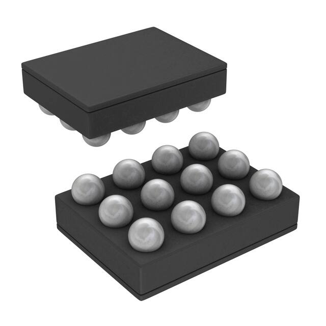
The LM2757 device comes in a tiny 12-pin 0.4-mm
pitch DSBGA package. A perfect fit for spaceconstrained, battery-operated applications, the device
requires only 4 small, inexpensive ceramic
capacitors. Built-in soft-start, overcurrent protection,
and thermal shutdown features are also included in
this device.
Device Information(1)
PART NUMBER
LM2757
PACKAGE
DSBGA (12)
BODY SIZE (MAX)
1.641 mm × 1.581 mm
(1) For all available packages, see the orderable addendum at
the end of the data sheet.
Typical Application
VIN = 3 V - 5.5 V
VIN
B2,B3
CIN
A3
1 µF
VOUT
VOUT = 4.1 V (100 mA), 4.5 V (110 mA)
5 V (180 mA)
A2
C1+
1 µF
COUT
C1
0.47 µF
B1
A1
C1C2+
LM2757
M0
C2
0.47 µF
M1
C3
C2-
GND
D3
D2
C1,C2
*Bump D1 is No Connect (NC)
1
An IMPORTANT NOTICE at the end of this data sheet addresses availability, warranty, changes, use in safety-critical applications,
intellectual property matters and other important disclaimers. PRODUCTION DATA.
�LM2757
SNVS536F – OCTOBER 2007 – REVISED JULY 2015
www.ti.com
Table of Contents
1
2
3
4
5
6
7
8
Features ..................................................................
Applications ...........................................................
Description .............................................................
Revision History.....................................................
Device Options.......................................................
Pin Configuration and Functions .........................
Specifications.........................................................
1
1
1
2
3
3
4
7.1
7.2
7.3
7.4
7.5
7.6
4
4
4
4
5
6
Absolute Maximum Ratings ......................................
ESD Ratings..............................................................
Recommended Operating Conditions.......................
Thermal Information ..................................................
Electrical Characteristics...........................................
Typical Characteristics ..............................................
Detailed Description ............................................ 10
8.1 Overview ................................................................. 10
8.2 Functional Block Diagram ....................................... 10
8.3 Feature Description................................................. 10
8.4 Device Functional Modes........................................ 11
9
Application and Implementation ........................ 13
9.1 Application Information............................................ 13
9.2 Typical Application ................................................. 13
10 Power Supply Recommendations ..................... 18
11 Layout................................................................... 19
11.1 Layout Guidelines ................................................. 19
11.2 Layout Example .................................................... 19
12 Device and Documentation Support ................. 20
12.1
12.2
12.3
12.4
12.5
12.6
Device Support ....................................................
Documentation Support ........................................
Community Resources..........................................
Trademarks ...........................................................
Electrostatic Discharge Caution ............................
Glossary ................................................................
20
20
20
20
20
20
13 Mechanical, Packaging, and Orderable
Information ........................................................... 21
4 Revision History
NOTE: Page numbers for previous revisions may differ from page numbers in the current version.
Changes from Revision E (May 2013) to Revision F
•
Added Device Information and Pin Configuration and Functions sections, ESD Rating table, Feature Description,
Device Functional Modes, Application and Implementation, Power Supply Recommendations, Layout, Device and
Documentation Support , and Mechanical, Packaging, and Orderable Information sections. ............................................... 1
Changes from Revision D (May 2013) to Revision E
•
2
Page
Page
Changed layout of National Data Sheet to TI format ........................................................................................................... 18
Submit Documentation Feedback
Copyright © 2007–2015, Texas Instruments Incorporated
Product Folder Links: LM2757
�LM2757
www.ti.com
SNVS536F – OCTOBER 2007 – REVISED JULY 2015
5 Device Options
Table 1. Mode Selection Definition
M0
M1
OUTPUT VOLTAGE MODE
0
0
Device shutdown, output high impedance
0
1
5V
1
0
4.5 V
1
1
4.1 V
6 Pin Configuration and Functions
YFQ Package
12-Pin DSBGA
Top View (left); Bottom View (right)
A1
A2
A3
A3
A2
A1
B1
B2
B3
B3
B2
B1
C1
C2
C3
C3
C2
C1
D1
D2
D3
D3
D2
D1
Pin Functions
PIN
NUMBER
NAME
TYPE
DESCRIPTION
A1
C2+
Power
Flying Capacitor C2 Connection
A2
VOUT
Power
Regulated Output Voltage
A3
C1+
Power
Flying Capacitor C1 Connection
B1
C1−
Power
Flying Capacitor C1 Connection
B2
VIN
Power
Input Voltage Connection
B3
VIN
Power
Input Voltage Connection
C1
GND
Ground
Ground Connection
C2
GND
Ground
Ground Connection
C3
C2−
Ground
Flying Capacitor C2 Connection
D1
NC
NC
D2
M1
Logic input
Mode select pin 1
D3
M0
Logic input
Mode select pin 0
No Connect — Do not connect this pin to any node, voltage or GND. Must be left floating.
Submit Documentation Feedback
Copyright © 2007–2015, Texas Instruments Incorporated
Product Folder Links: LM2757
3
�LM2757
SNVS536F – OCTOBER 2007 – REVISED JULY 2015
www.ti.com
7 Specifications
7.1 Absolute Maximum Ratings
over operating free-air temperature range (unless otherwise noted) (1) (2) (3)
MIN
MAX
UNIT
VIN pin: voltage to GND
–0.3
6
V
M0, M1 pins: voltage to GND
–0.3
6
V
Continuous power dissipation (4)
Internally Limited
Junction temperature, TJ-MAX
Maximum lead temperature (soldering, 10 sec.)
Storage temperature, Tstg
(1)
(2)
(3)
(4)
–65
150
°C
265
°C
150
°C
Stresses beyond those listed under Absolute Maximum Ratings may cause permanent damage to the device. These are stress ratings
only, which do not imply functional operation of the device at these or any other conditions beyond those indicated under Recommended
Operating Conditions. Exposure to absolute-maximum-rated conditions for extended periods may affect device reliability.
If Military/Aerospace specified devices are required, please contact the TI Sales Office/ Distributors for availability and specifications.
All voltages are with respect to the potential at the GND pins.
Internal thermal shutdown circuitry protects the device from permanent damage. Thermal shutdown engages at TJ = 145°C (typical) and
disengages at TJ = 135°C (typical).
7.2 ESD Ratings
V(ESD)
(1)
Electrostatic discharge
VALUE
UNIT
±2500
V
Human-body model (HBM), per ANSI/ESDA/JEDEC JS-001 (1)
JEDEC document JEP155 states that 500-V HBM allows safe manufacturing with a standard ESD control process.
7.3 Recommended Operating Conditions
over operating free-air temperature range (unless otherwise noted) (1) (2)
MIN
NOM
MAX
UNIT
Input voltage
2.7
5.5
°C
Junction temperature, TJ
–30
110
°C
–30
85
°C
Ambient temperature, TA
(1)
(2)
(3)
(3)
Stresses beyond those listed under Absolute Maximum Ratings may cause permanent damage to the device. These are stress ratings
only, which do not imply functional operation of the device at these or any other conditions beyond those indicated under Recommended
Operating Conditions. Exposure to absolute-maximum-rated conditions for extended periods may affect device reliability.
All voltages are with respect to the potential at the GND pins.
In applications where high power dissipation and/or poor package thermal resistance is present, the maximum ambient temperature may
have to be derated. Maximum ambient temperature (TA-MAX) is dependent on the maximum operating junction temperature (TJMAX-OP =
125°C), the maximum power dissipation of the device in the application (PD-MAX), and the junction-to-ambient thermal resistance of the
part/package in the application (RθJA), as given by the following equation: TA-MAX = TJ-MAX-OP – (RθJA × PD-MAX).
7.4 Thermal Information
LM2757
THERMAL METRIC (1)
YFQ (DSBGA)
UNIT
12 PINS
RθJA
(1)
4
Junction-to-ambient thermal resistance
75
°C/W
For more information about traditional and new thermal metrics, see the Semiconductor and IC Package Thermal Metrics application
report, SPRA953.
Submit Documentation Feedback
Copyright © 2007–2015, Texas Instruments Incorporated
Product Folder Links: LM2757
�LM2757
www.ti.com
SNVS536F – OCTOBER 2007 – REVISED JULY 2015
7.5 Electrical Characteristics
Unless otherwise specified, typical (TYP) limits in apply for TA = 25ºC; minimium (MIN) and maximum (MAX) limits apply over
the full operating ambient temperature range (–30°C ≤ TA ≤ +85°C) . Unless otherwise noted, specifications apply to Typical
Application with: VIN = 3.6 V, V(M0) = 0 V, V(M1) = VIN, CIN = C2 = 0.47 µF, CIN= COUT = 1 µF. (1) (2) (3)
PARAMETER
VOUT
IQ
Output voltage
Quiescent supply current
MIN
TYP
MAX
3.2 V ≤ VIN ≤ 5.5 V
–30°C ≤ TA ≤ +60°C
IOUT = 0 to 180 mA
V(M0) = 0V, V(M1) = VIN
TEST CONDITIONS
4.870
(−2.6%)
5
5.130
(2.6%)
3. V ≤ VIN ≤ 5.5 V
–30°C ≤ TA ≤ +85°C
IOUT = 0 to 150 mA
V(M0) = 0V, V(M1) = VIN
4.865
(−2.7%)
5
5.130
(2.6%)
3 V ≤ VIN ≤ 5.5 V
IOUT = 0 to 110 mA
V(M0) = VIN, V(M1) = 0 V
4.406
(–2.1%)
4.5
4.613
(2.5%)
3. V ≤ VIN ≤ 5.5 V
IOUT = 0 to 100 mA
V(M0) = VIN, V(M1) = VIN
3.985
(–2.8%)
4.1
4.223
(3%)
V(M0) = 0 V, V(M1) = VIN (5 V)
IOUT = 0 mA
VIN = 3.6 V
2.4
2.79
V(M0) = VIN, V(M1) = 0 V (4.5 V)
IOUT = 0 mA
VIN = 3.6 V
1.5
1.80
V(M0) = VIN, V(M1) = VIN (4.1 V)
IOUT = 0 mA
VIN = 3.6 V
1.3
1.65
2
UNIT
V
mA
ISD
Shutdown supply current
V(M0) = 0 V, V(M1) = 0 V
VIN = 3.6 V
1.1
VR
Output ivoltage rpple
IOUT = 150 mA
V(M0) = 0V, V(M1) = VIN (5 V)
3 V ≤ VIN ≤ 5.5 V
20
ƒSW
Switching frequency
3 V ≤ VIN ≤ 5.5 V
VIN
Logic input high
Input pins: M1, M0
3 V ≤ VIN ≤ 5.5 V
1
VIN
V
VIL
Logic input low
Input pins: M1, M0
3 V ≤ VIN ≤ 5.5 V
0
0.40
V
RPULLDOWN
Logic input pulldown
resistance (M0, M1)
V(M1, M0) = 5.5 V
324
IIH
Logic input high current
Input Pins: M1, M0
V(M1, M0) = 1.8 V (4)
IIL
Logic input low current
Input Pins: M1, M0
V(M1, M0) = 0 V
VG
Gain transition voltage
ISC
Short-circuit output current
ION
VOUT turnon time from
shutdown (5)
(1)
(2)
(3)
(4)
(5)
0.932
(–25%)
1.242
µA
mVp–p
1.552
(+25%)
MHz
457
kΩ
5
µA
10
nA
1.5× to 2×, V(M0) = VIN, V(M1) = 0 V
3.333
V
2× to 1.5×, V(M0) = VIN, V(M1) = 0 V
3.413
Hysteresis, V(M0) = VIN, V(M1) = 0 V
80
1.5× to 2×, V(M0) = 0 V, V(M1) = VIN
3.87
2× to 1.5×, V(M0) = 0 V, V(M1) = VIN
3.93
Hysteresis, V(M0) = 0 V, V(M1) = VIN
60
mV
250
mA
300
µs
VOUT = 0 V
V
mV
V
V
All voltages are with respect to the potential at the GND pins.
Minimum and maximum limits are specified by design, test, or statistical analysis. Typical numbers are not ensured, but do represent the
most likely norm.
CIN, COUT, C1, C2: Low-ESR Surface-Mount Ceramic Capacitors (MLCCs) used in setting electrical characteristics.
There is a 450-kΩ (typical) pulldown resistor connected internally to each logic input.
Turnon time is measured from when the M0 or M1 signal is pulled high until the output voltage crosses 90% of its final value.
Submit Documentation Feedback
Copyright © 2007–2015, Texas Instruments Incorporated
Product Folder Links: LM2757
5
�LM2757
SNVS536F – OCTOBER 2007 – REVISED JULY 2015
www.ti.com
7.6 Typical Characteristics
Unless otherwise specified: VIN = 3.6 V, V(M0) = 0 V, V(M1) = VIN, C1 = C2 = 0.47 µF, CIN = COUT = 1 µF, TA = 25°C.
Capacitors are low-ESR multi-layer ceramic capacitors (MLCC's).
5-V Mode
4.5-V Mode
Figure 1. Efficiency vs. Input Voltage
4.1-V Mode
5-V Mode
Figure 3. Efficiency vs. Input Voltage
4.5-V Mode
Figure 4. Output Voltage vs. Output Current
4.1-V Mode
Figure 5. Output Voltage vs. Output Current
6
Figure 2. Efficiency vs. Input Voltage
Figure 6. Output Voltage vs. Output Current
Submit Documentation Feedback
Copyright © 2007–2015, Texas Instruments Incorporated
Product Folder Links: LM2757
�LM2757
www.ti.com
SNVS536F – OCTOBER 2007 – REVISED JULY 2015
Typical Characteristics (continued)
Unless otherwise specified: VIN = 3.6 V, V(M0) = 0 V, V(M1) = VIN, C1 = C2 = 0.47 µF, CIN = COUT = 1 µF, TA = 25°C.
Capacitors are low-ESR multi-layer ceramic capacitors (MLCC's).
5-V Mode
5-V Mode
Figure 7. Output Voltage Ripple vs. Output Current
4.5-V Mode
Figure 8. Output Voltage vs. Input Voltage
4.1-V Mode
Figure 9. Output Voltage vs. Input Voltage
Figure 10. Output Voltage vs. Input Voltage
Figure 11. Output Leakage Current, Device Shutdown
Figure 12. Output Leakage Current, Device Shutdown
Submit Documentation Feedback
Copyright © 2007–2015, Texas Instruments Incorporated
Product Folder Links: LM2757
7
�LM2757
SNVS536F – OCTOBER 2007 – REVISED JULY 2015
www.ti.com
Typical Characteristics (continued)
Unless otherwise specified: VIN = 3.6 V, V(M0) = 0 V, V(M1) = VIN, C1 = C2 = 0.47 µF, CIN = COUT = 1 µF, TA = 25°C.
Capacitors are low-ESR multi-layer ceramic capacitors (MLCC's).
Figure 13. Current Limit vs. Input Voltage
Figure 14. Oscillator Frequency vs. Input Voltage
Figure 15. Operating Current vs. Input Voltage
Figure 16. Shutdown Supply Current vs. Input Voltage
VIN = 3.6 V
Load = 200 mA
Time scale: 100 µs/Div
CH2: VOUT; Scale: 1V/Div, DC Coupled
CH4: IIN; Scale: 200 mA/Div, DC Coupled
VOUT = 5-V Mode
Load = 200 mA
Time scale: 100 µs/Div
CH1: VIN; Scale: 1V/Div, DC Coupled
CH2: VOUT; Scale: 100mV/Div, AC Coupled
Figure 17. Start-up Behavior, 5-V Mode
8
Submit Documentation Feedback
Figure 18. Line Step, 3.5 V to 4 V
Copyright © 2007–2015, Texas Instruments Incorporated
Product Folder Links: LM2757
�LM2757
www.ti.com
SNVS536F – OCTOBER 2007 – REVISED JULY 2015
Typical Characteristics (continued)
Unless otherwise specified: VIN = 3.6 V, V(M0) = 0 V, V(M1) = VIN, C1 = C2 = 0.47 µF, CIN = COUT = 1 µF, TA = 25°C.
Capacitors are low-ESR multi-layer ceramic capacitors (MLCC's).
VOUT = 5-V Mode
VBATT = 4 V
Time scale: 10 µs/Div
CH1: VOUT; Scale: 50mV/Div, AC Coupled
CH4: IOUT; Scale: 100mA/Div, DC Coupled
Figure 19. Load Step With Li-Ion Battery, 10 mA to 200 mA
VOUT = 5-V Mode
VBATT = 4 V
Time scale: 10 µs/Div
CH1: VOUT; Scale: 50mV/Div, AC Coupled
CH4: IOUT; Scale: 100mA/Div, DC Coupled
Figure 20. Load Step With Li-Ion Battery 200 mA to 10 mA
Submit Documentation Feedback
Copyright © 2007–2015, Texas Instruments Incorporated
Product Folder Links: LM2757
9
�LM2757
SNVS536F – OCTOBER 2007 – REVISED JULY 2015
www.ti.com
8 Detailed Description
8.1 Overview
The LM2757 is a switched capacitor converter that produces a regulated output voltage of either 5 V, 4.5 V or
4.1 V, depending on the mode selected. The core of the part is a highly efficient charge pump that utilizes fixed
frequency pre-regulation to minimize ripple and power losses over wide input voltage and output current ranges.
A description of the principal operational characteristics of the LM2757 is shown in the Functional Block Diagram
and detailed in Feature Description.
8.2 Functional Block Diagram
VIN
C1+
GAIN
CONTROL
V Ref
SWITCH
CONTROL
SWITCH
ARRAY
3
G= 2, 2
C1C2+
C2VOUT
OSCILLATOR
SHORTCIRCUIT
PROTECTION
EN
THERMAL
SHUTDOWN
M0
M1
VOLTAGE MODE
SELECT AND
ENABLE CONTROL
1.24 V
Ref.
Soft-Start
Ramp
GND
8.3 Feature Description
The core of the LM2757 is a two-phase charge pump controlled by an internally generated non-overlapping
clock. The charge pump operates by using external flying capacitors C1 and C2 to transfer charge from the input
to the output. At input voltages below 3.9 V (typical) for the 5-V mode, the LM2757 operates in a 2× gain, with
the input current being equal to 2× the load current. At input voltages above 3.9 V (typical) for the 5-V mode, the
part utilizes a gain of 3/2×, resulting in an input current equal to 3/2 times the load current. For the 4.5-V mode,
the LM2757 operates in a 2× gain when the input voltage is below 3.35 V (typical) and transitions to a 3/2× gain
when the input voltage is above 3.35 V (typical). For the 4.1-V mode, the device utilizes the 3/2× gain for the
entire input voltage range.
The two phases of the switched capacitor switching cycle are referred to as the phase one and the phase two.
During phase one, one flying capacitor is charged by the input supply while the other flying capacitor is
connected to the output and delivers charge to the load . After half of the switching cycle [ t = 1/(2 × ƒSW)], the
LM2757 switches to phase two. In this configuration, the capacitor that supplied charge to the load in phase one
is connected to the input to be recharged while the capacitor that had been charged in the previous phase is
connected to the output to deliver charge. With this topology, output ripple is reduced by delivering charge to the
output in every phase.
10
Submit Documentation Feedback
Copyright © 2007–2015, Texas Instruments Incorporated
Product Folder Links: LM2757
�LM2757
www.ti.com
SNVS536F – OCTOBER 2007 – REVISED JULY 2015
Feature Description (continued)
The LM2757 uses fixed frequency pre-regulation to regulate the output voltage. The input and output
connections of the flying capacitors are made with internal MOS switches. Pre-regulation limits the gate drive of
the MOS switch connected between the voltage input and the flying capacitors. Controlling the on resistance of
this switch limits the amount of charge transferred into and out of each flying capacitor during the charge and
discharge phases, and in turn helps to keep the output ripple very low.
8.3.1 Efficiency Performance
Charge-pump efficiency is derived in Equation 1 and Equation 2 (supply current and other losses are neglected
for simplicity):
IIN = G × IOUT
E = (VOUT × IOUT) ÷ (VIN × IIN) = VOUT ÷ (G × VIN)
(1)
where
•
•
G = the charge pump gain
E = efficiency
(2)
Efficiency is at its highest as G × VIN approaches VOUT. Refer to Typical Characteristics for detailed efficiency
data. The transition between gains of 3/2 and 2 are clearly distinguished by the sharp discontinuity in the
efficiency curve.
8.3.2 Soft Start
The LM2757 employs soft-start circuitry to prevent excessive input inrush currents during start-up. At start-up,
the output voltage gradually rises from 0 V to the nominal output voltage. This occurs in 300 µs (typical). Softstart is engaged when the device is enabled.
8.3.3 Thermal Shutdown
Protection from damage related to overheating is achieved with a thermal shutdown feature. When the junction
temperature rises to 145°C (typical), the device switches into shutdown mode. The LM2757 disengages thermal
shutdown when the junction temperature of the part is reduced to 135°C (typical). Due to the high efficiency of
the LM2757, thermal shutdown and/or thermal cycling are not encountered when the part is operated within
specified input voltage, output current, and ambient temperature operating ratings. If thermal cycling is seen
under these conditions, the most likely cause is an inadequate PCB layout that does not allow heat to be
sufficiently dissipated out of the device.
8.3.4 Current-Limit Protection
The LM2757 charge pump contains current-limit protection circuitry that protects the device during VOUT fault
conditions where excessive current is drawn. Output current is limited to 250 mA (typical).
8.4 Device Functional Modes
8.4.1 Enable and Voltage Mode Selection
The LM2757 is enabled when either one of the mode select pins (M0, M1) has a logic High voltage applied to it.
There are 450-kΩ pulldown resistors connected internally to each of the mode select pins. The voltage mode is
selected according to Table 1.
Submit Documentation Feedback
Copyright © 2007–2015, Texas Instruments Incorporated
Product Folder Links: LM2757
11
�LM2757
SNVS536F – OCTOBER 2007 – REVISED JULY 2015
www.ti.com
Device Functional Modes (continued)
8.4.2 Shutdown With Output High Impedance
The LM2757 is in shutdown mode when there is a logic Low voltage on both mode select pins (M0, M1). There
are also 450-kΩ pulldown resistors connected to both mode select pins, pulling the nodes down to ground when
there is no signal present. When in shutdown, the output of the LM2757 is high impedance, allowing an external
supply to drive the output line such as in USB OTG or mobile HDMI applications. Refer to the output leakage
current graphs in Typical Characteristics for typical leakage currents into the VOUT pin, when driven by a
separate supply during shutdown. Output leakage increases with temperature, with the lowest leakage occurring
at –30°C and the highest leakage at 85°C (on which the graph is based). It should be noted when looking at the
graphs as the input voltage falls the leakage peaks at around an input voltage of 1.5 V, then goes down as the
input voltage decrease to 0 V. The leakage at an input voltage of 0 V is the same as the leakage current when
the battery is disconnected from the circuit.
12
Submit Documentation Feedback
Copyright © 2007–2015, Texas Instruments Incorporated
Product Folder Links: LM2757
�LM2757
www.ti.com
SNVS536F – OCTOBER 2007 – REVISED JULY 2015
9 Application and Implementation
NOTE
Information in the following applications sections is not part of the TI component
specification, and TI does not warrant its accuracy or completeness. TI’s customers are
responsible for determining suitability of components for their purposes. Customers should
validate and test their design implementation to confirm system functionality.
9.1 Application Information
The LM2757 can create a 4.1-V, 4.5-V or 5-V system rail capable of delivering up to 180 mA of output current to
the load. The 1.242-MHz switched capacitor boost allows for the use of small value discrete external
components.
9.2 Typical Application
9.2.1 Switched-Capacitor Boost Regulator
VIN = 3 V - 5.5 V
VIN
B2,B3
CIN
A3
1 µF
VOUT
VOUT = 4.1 V (100 mA), 4.5 V (110 mA)
5 V (180 mA)
A2
C1+
COUT
1 µF
C1
0.47 µF
B1
A1
C1C2+
LM2757
M0
C2
0.47 µF
M1
C3
C2-
GND
D3
D2
C1,C2
*Bump D1 is No Connect (NC)
Figure 21. LM2757 Typical Application
9.2.1.1 Design Requirements
Example requirements for typical switched-capacitor boost regulator applications:
Table 2. Design Parameters
DESIGN PARAMETER
EXAMPLE VALUE
Input voltage range
2.7 V to 5.5 V
Output current
0 to 180 mA
Boost switching frequency
1.242 MHz
9.2.1.2 Detailed Design Procedure
9.2.1.2.1 Recommended Capacitor Types
The LM2757 requires 4 external capacitors for proper operation. Surface-mount multi-layer ceramic capacitors
are recommended. These capacitors are small, inexpensive and have very low equivalent series resistance
(ESR, ≤ 15 mΩ typical). Tantalum capacitors, OS-CON capacitors, and aluminum electrolytic capacitors
generally are not recommended for use with the LM2757 due to their high ESR, as compared to ceramic
capacitors.
For most applications, ceramic capacitors with an X7R or X5R temperature characteristic are preferred for use
with the LM2757. These capacitors have tight capacitance tolerance (as good as ±10%) and hold their value over
temperature (X7R: ±15% over –55°C to 125°C; X5R: ±15% over –55°C to 85°C).
Submit Documentation Feedback
Copyright © 2007–2015, Texas Instruments Incorporated
Product Folder Links: LM2757
13
�LM2757
SNVS536F – OCTOBER 2007 – REVISED JULY 2015
www.ti.com
Capacitors with a Y5V or Z5U temperature characteristic are generally not recommended for use with the
LM2757. These types of capacitors typically have wide capacitance tolerance (80%, –20%) and vary significantly
over temperature (Y5V: +22%, –82% over –30°C to +85°C range; Z5U: 22%, –56% over a 10°C to 85°C range).
Under some conditions, a 1-µF-rated Y5V or Z5U capacitor could have a capacitance as low as 0.1 µF. Such
detrimental deviation is likely to cause Y5V and Z5U capacitors to fail to meet the minimum capacitance
requirements of the LM2757.
Net capacitance of a ceramic capacitor decreases with increased DC bias. This degradation can result in lower
capacitance than expected on the input and/or output, resulting in higher ripple voltages and currents. Using
capacitors at DC bias voltages significantly below the capacitor voltage rating usually minimizes DC bias effects.
Consult capacitor manufacturers for information on capacitor DC bias characteristics.
Capacitance characteristics can vary quite dramatically with different application conditions, capacitor types, and
capacitor manufacturers. It is strongly recommended that the LM2757 circuit be thoroughly evaluated early in the
design-in process with the mass-production capacitors of choice. This helps ensure that any such variability in
capacitance does not negatively impact circuit performance.
The voltage rating of the output capacitor should be 10 V or more. For example, a 10-V 0603 1-µF capacitor is
acceptable for use with the LM2757, as long as the capacitance does not fall below a minimum of 0.5 µF in the
intended application. All other capacitors should have a voltage rating at or above the maximum input voltage of
the application. The capacitors should be selected such that the capacitance on the input does not fall below 0.7
µF, and the capacitance of the flying capacitors does not fall below 0.2 µF.
Table 3 lists some leading ceramic capacitor manufacturers.
Table 3. Manufacturers of Suggested Capacitors
MANUFACTURER
CONTACT INFORMATION
AVX
www.avx.com
Murata
www.murata.com
Taiyo-Yuden
www.t-yuden.com
TDK
www.component.tdk.com
Vishay-Vitramon
www.vishay.com
9.2.1.2.2 Output Capacitor And Output Voltage Ripple
The output capacitor in the LM2757 circuit (COUT) directly impacts the magnitude of output voltage ripple. Other
prominent factors also affecting output voltage ripple include input voltage, output current, and flying capacitance.
Due to the complexity of the regulation topology, providing equations or models to approximate the magnitude of
the ripple can not be easily accomplished. But one important generalization can be made: increasing
(decreasing) the output capacitance results in a proportional decrease (increase) in output voltage ripple.
In typical high-current applications, a 1-µF low-ESR ceramic output capacitor is recommended. Different output
capacitance values can be used to reduce ripple, shrink the solution size, and/or cut the cost of the solution. But
changing the output capacitor may also require changing the flying capacitor and/or input capacitor to maintain
good overall circuit performance. Performance of the LM2757 with different capacitor setups in discussed in
Recommended Capacitance.
High ESR in the output capacitor increases output voltage ripple. If a ceramic capacitor is used at the output, this
is usually not a concern because the ESR of a ceramic capacitor is typically very low and has only a minimal
impact on ripple magnitudes. If a different capacitor type with higher ESR is used (tantalum, for example), the
ESR could result in high ripple. To eliminate this effect, the net output ESR can be significantly reduced by
placing a low-ESR ceramic capacitor in parallel with the primary output capacitor. The low ESR of the ceramic
capacitor is in parallel with the higher ESR, resulting in a low net ESR based on the principles of parallel
resistance reduction.
9.2.1.2.3 Input Capacitor And Input Voltage Ripple
The input capacitor (CIN) is a reservoir of charge that aids a quick transfer of charge from the supply to the flying
capacitors during the charge phase of operation. The input capacitor helps to keep the input voltage from
drooping at the start of the charge phase when the flying capacitors are connected to the input. It also filters
noise on the input pin, keeping this noise out of sensitive internal analog circuitry that is biased off the input line.
14
Submit Documentation Feedback
Copyright © 2007–2015, Texas Instruments Incorporated
Product Folder Links: LM2757
�LM2757
www.ti.com
SNVS536F – OCTOBER 2007 – REVISED JULY 2015
Much like the relationship between the output capacitance and output voltage ripple, input capacitance has a
dominant and first-order effect on input ripple magnitude. Increasing (decreasing) the input capacitance results in
a proportional decrease (increase) in input voltage ripple. Input voltage, output current, and flying capacitance
also affects input ripple levels to some degree.
In typical high-current applications, a 1-µF low-ESR ceramic capacitor is recommended on the input. Different
input capacitance values can be used to reduce ripple, shrink the solution size, and/or cut the cost of the
solution. But changing the input capacitor may also require changing the flying capacitor and/or output capacitor
to maintain good overall circuit performance. Performance of the LM2757 with different capacitor setups is
discussed in Recommended Capacitance.
9.2.1.2.4 Flying Capacitors
The flying capacitors (C1, C2) transfer charge from the input to the output. Flying capacitance can impact both
output current capability and ripple magnitudes. If flying capacitance is too small, the LM2757 may not be able to
regulate the output voltage when load currents are high. On the other hand, if the flying capacitance is too large,
the flying capacitor might overwhelm the input and output capacitors, resulting in increased input and output
ripple.
In typical high-current applications, 0.47-µF low-ESR ceramic capacitors are recommended for the flying
capacitors. Polarized capacitors (tantalum, aluminum electrolytic, etc.) must not be used for the flying capacitor,
as they could become reverse-biased during LM2757 operation.
9.2.1.2.5 Recommended Capacitance
The data in Table 4 can be used to assist in the selection of capacitance for each node that best balances
solution size and cost with the electrical requirements of the application.
As previously discussed, input and output ripple voltages varies with output current and input voltage. The
numbers provided show expected ripple voltage with VIN = 3.6 V and a load current of 200 mA at 5-V output, 100
mA at 4.5-V output, and 100 mA at 4.1-V output. Table 4 offers a first look at approximate ripple levels and
provides a comparison of different capacitance configurations, but is not intended to ensure performance. With
any capacitance configuration chosen, always verify that the performance of the ripple waveforms are suitable for
the intended application. The same capacitance value must be used for all the flying capacitors. For output
regulation performance with different capacitor configurations, please refer to the output voltage vs. input voltage
graphs in Typical Characteristics. The output voltage regulation is typically better when using capacitors with a
higher capacitance value and a higher voltage bias rating than the nominal voltage applied to them, as can be
seen in the graphs, but this may have an impact in capacitor case size. For typical high-current small solution
size applications, 1-µF capacitance X5R temperature characteristic rating 0402 (C1005) case size and 10-V bias
or higher capacitors can be used for the input, output and flying capacitors. According to current capacitor
offerings, there are no capacitors in the 0201 (C0603) case size that satisfy the minimum capacitance
requirements of the LM2757 circuit. When selecting capacitors, those with the highest voltage bias rating
available from the capacitor supplier are preferred.
Table 4. LM2757 Performance With Different Capacitor Configurations (1)
CAPACITOR CONFIGURATION
(VIN = 3.6 V)
5-V, 200-mA OUTPUT
RIPPLE (mV)(typical)
4.5-V, 100-mA OUTPUT
RIPPLE (mV) (typical)
4.1-V, 100-mA OUTPUT
RIPPLE (mV)(typical)
CIN = 1 µF, COUT = 1 µF, C1 and C2 = 0.47 µF
32
12
11
CIN = 0.68 µF, COUT = 1 µF, C1 and C2 = 0.47 µF
32
11
11
CIN = 0.68 µF, COUT = 0.47 µF, C1 and C2 = 0.47 µF
51
151
15
CIN = 0.68 µF, COUT = 0.47 µF, C1 and C2 = 0.22 µF
53
181
18
(1)
Refer to the text in Recommended Capacitance for detailed information on the data in this table.
Submit Documentation Feedback
Copyright © 2007–2015, Texas Instruments Incorporated
Product Folder Links: LM2757
15
�LM2757
SNVS536F – OCTOBER 2007 – REVISED JULY 2015
www.ti.com
9.2.1.3 Application Curves
5-V Mode
4.5-V Mode
Figure 22. Efficiency vs. Input Voltage
Figure 23. Efficiency vs. Input Voltage
4.1-V Mode
Figure 24. Efficiency vs. Input Voltage
9.2.2 USB OTG / Mobile HDMI Power Supply
The 5-V output mode is normally used for the USB OTG / Mobile HDMI application. Therefore, the LM2757 can
be enabled or disabled by applying a logic signal on only the M1 pin while grounding the M0 pin. Depending on
the USB/HDMI mode of the application, the LM2757 can be enabled to drive the power bus line (Host), or
disabled to put its output in high impedance allowing an external supply to drive the bus line (Slave). In addition
to the high-impedance backdrive protection, the output current limit protection is 250 mA (typical), well within the
USB OTG and HDMI requirements.
16
Submit Documentation Feedback
Copyright © 2007–2015, Texas Instruments Incorporated
Product Folder Links: LM2757
�LM2757
www.ti.com
SNVS536F – OCTOBER 2007 – REVISED JULY 2015
VBAT (System Voltage)
EN (VM1)
LM2757 (Host
Mode VBUS
Power)
USB Connector
VM0
VOUT / VBUS (5V)
VBUS
Dual Role
Application
Processor
ID
D+
D-
USB OTG
Transceiver
GND
Figure 25. USB OTG / Mobile HDMI
9.2.3 Supercapacitor Flash Driver
Using the 5-V output voltage mode, the LM2757 can charge a supercapacitor for LED flash applications while
limiting the peak current drawn off the battery during the charge cycle. The LM2757 can be disabled for the Flash
event, placing its output in high impedance with the input. In this way, all charge for the flash LED(s) comes
directly off the supercapacitor and does not load the main battery line. The LM2757 can be enabled or disabled
by applying a logic signal on only the M1 pin while grounding the M0 pin.
Special consideration must be given when using supercapacitors for LED flash applications where the voltage on
the capacitor is charged to a fixed value. This is due to the possible power management issues that can arise as
a result of the high flash current and wide tolerance ranges (V–I characteristics) of typical flash LEDs. If the
voltage across the Flash LED(s) is not managed, damage may occur where a relatively low Vf LED is overdriven
or places excessive voltage across the bottom control FET. To help avoid this issue, the use of a high-power
current sink is advised in applications where the forward voltage specification of the flash LED has a wide range.
VOUT = 5V
VBAT
Charge (M1)
LM2757
Supercapacitor
Flash Charger
Flash
LED(s)
2.7 k:
R
R
M0
2.7 k:
0.6F, 5V, Dual
Supercapacitor
Flash
Figure 26. Supercapacitor Flash Driver
Submit Documentation Feedback
Copyright © 2007–2015, Texas Instruments Incorporated
Product Folder Links: LM2757
17
�LM2757
SNVS536F – OCTOBER 2007 – REVISED JULY 2015
www.ti.com
9.2.4 LED Driver
The 5-V, 4.5-V, or the 4.1-V mode can be used depending on the forward voltage and load requirements of the
LED application. The LM2757 can be enabled or disabled by applying the appropriate combination of logic
signals on the M1 and M0 pins. LED current for each string in this application is limited by the voltage across the
string's ballast resistor, which is dependent on the output voltage mode selected and the V-I profile of each LED
used.
VOUT = 4.1V (100 mA), 4.5V (110 mA)
5.0V (180 mA)
VBAT
M0
M1
LM2757
LED
Driver
LED(s)
D1
DX
R
R
Figure 27. LED Driver
10 Power Supply Recommendations
The LM2757 is designed to operate as an inverter over an input voltage supply range between 2.7 V and 5.5 V.
18
Submit Documentation Feedback
Copyright © 2007–2015, Texas Instruments Incorporated
Product Folder Links: LM2757
�LM2757
www.ti.com
SNVS536F – OCTOBER 2007 – REVISED JULY 2015
11 Layout
11.1 Layout Guidelines
Proper board layout helps to ensure optimal performance of the LM2757 circuit. The following guidelines are
recommended:
• Place capacitors as close to the LM2757 as possible, and preferably on the same side of the board as the
device.
• Use short, wide traces to connect the external capacitors to the LM2757 to minimize trace resistance and
inductance.
• Use a low resistance connection between ground and the GND pin of the LM2757. Using wide traces and/or
multiple vias to connect GND to a ground plane on the board is most advantageous.
11.2 Layout Example
VOUT
1 PF
C1+
1 PF
C2+
C1-
VIAs to
GND
Plane
C2+
VOUT
C1+
C1-
VIN
VIN
GND
GND
C2-
1 PF
VIN
C2-
GND
NC
M1
M0
M1
M0
1 PF
Figure 28. LM2757 Layout Example
Submit Documentation Feedback
Copyright © 2007–2015, Texas Instruments Incorporated
Product Folder Links: LM2757
19
�LM2757
SNVS536F – OCTOBER 2007 – REVISED JULY 2015
www.ti.com
12 Device and Documentation Support
12.1 Device Support
12.1.1 Third-Party Products Disclaimer
TI'S PUBLICATION OF INFORMATION REGARDING THIRD-PARTY PRODUCTS OR SERVICES DOES NOT
CONSTITUTE AN ENDORSEMENT REGARDING THE SUITABILITY OF SUCH PRODUCTS OR SERVICES
OR A WARRANTY, REPRESENTATION OR ENDORSEMENT OF SUCH PRODUCTS OR SERVICES, EITHER
ALONE OR IN COMBINATION WITH ANY TI PRODUCT OR SERVICE.
12.2 Documentation Support
12.2.1 Related Documentation
For related documentation see the following:
Texas Instruments Application Note 1112 DSBGA Wafer Level Chip Scale Package (SNVA009).
12.3 Community Resources
The following links connect to TI community resources. Linked contents are provided "AS IS" by the respective
contributors. They do not constitute TI specifications and do not necessarily reflect TI's views; see TI's Terms of
Use.
TI E2E™ Online Community TI's Engineer-to-Engineer (E2E) Community. Created to foster collaboration
among engineers. At e2e.ti.com, you can ask questions, share knowledge, explore ideas and help
solve problems with fellow engineers.
Design Support TI's Design Support Quickly find helpful E2E forums along with design support tools and
contact information for technical support.
12.4 Trademarks
E2E is a trademark of Texas Instruments.
All other trademarks are the property of their respective owners.
12.5 Electrostatic Discharge Caution
This integrated circuit can be damaged by ESD. Texas Instruments recommends that all integrated circuits be handled with
appropriate precautions. Failure to observe proper handling and installation procedures can cause damage.
ESD damage can range from subtle performance degradation to complete device failure. Precision integrated circuits may be more
susceptible to damage because very small parametric changes could cause the device not to meet its published specifications.
12.6 Glossary
SLYZ022 — TI Glossary.
This glossary lists and explains terms, acronyms, and definitions.
20
Submit Documentation Feedback
Copyright © 2007–2015, Texas Instruments Incorporated
Product Folder Links: LM2757
�LM2757
www.ti.com
SNVS536F – OCTOBER 2007 – REVISED JULY 2015
13 Mechanical, Packaging, and Orderable Information
The following pages include mechanical, packaging, and orderable information. This information is the most
current data available for the designated devices. This data is subject to change without notice and revision of
this document. For browser-based versions of this data sheet, refer to the left-hand navigation.
Submit Documentation Feedback
Copyright © 2007–2015, Texas Instruments Incorporated
Product Folder Links: LM2757
21
�PACKAGE OPTION ADDENDUM
www.ti.com
10-Dec-2020
PACKAGING INFORMATION
Orderable Device
Status
(1)
Package Type Package Pins Package
Drawing
Qty
Eco Plan
(2)
Lead finish/
Ball material
MSL Peak Temp
Op Temp (°C)
Device Marking
(3)
(4/5)
(6)
LM2757TM/NOPB
ACTIVE
DSBGA
YFQ
12
250
RoHS & Green
SNAGCU
Level-1-260C-UNLIM
-30 to 85
DL
LM2757TMX/NOPB
ACTIVE
DSBGA
YFQ
12
3000
RoHS & Green
SNAGCU
Level-1-260C-UNLIM
-30 to 85
DL
(1)
The marketing status values are defined as follows:
ACTIVE: Product device recommended for new designs.
LIFEBUY: TI has announced that the device will be discontinued, and a lifetime-buy period is in effect.
NRND: Not recommended for new designs. Device is in production to support existing customers, but TI does not recommend using this part in a new design.
PREVIEW: Device has been announced but is not in production. Samples may or may not be available.
OBSOLETE: TI has discontinued the production of the device.
(2)
RoHS: TI defines "RoHS" to mean semiconductor products that are compliant with the current EU RoHS requirements for all 10 RoHS substances, including the requirement that RoHS substance
do not exceed 0.1% by weight in homogeneous materials. Where designed to be soldered at high temperatures, "RoHS" products are suitable for use in specified lead-free processes. TI may
reference these types of products as "Pb-Free".
RoHS Exempt: TI defines "RoHS Exempt" to mean products that contain lead but are compliant with EU RoHS pursuant to a specific EU RoHS exemption.
Green: TI defines "Green" to mean the content of Chlorine (Cl) and Bromine (Br) based flame retardants meet JS709B low halogen requirements of