LM2772
www.ti.com
SNVS486B – DECEMBER 2006 – REVISED MAY 2013
LM2772 Low-Ripple Switched Capacitor Step-Down Regulator
Check for Samples: LM2772
FEATURES
DESCRIPTION
•
•
•
•
•
•
•
•
•
•
•
•
The LM2772 is a switched capacitor step-down
regulator that produces a 1.2V output. It is capable of
supplying loads up to 150mA with 3% output voltage
regulation over line, load, and temperature. The
LM2772 operates with an input voltage from 3.0V to
5.5V, accommodating 1-cell Li-Ion batteries and
chargers.
1
2
Low-Noise Fixed Frequency Operation
1.2V Output Voltage
3% Output Voltage Regulation
Li-Ion (3.6V) to 1.2V with 80% Efficiency
Very Low Output Ripple: 8mV @ 150mA
Output Currents up to 150mA
2.7V to 5.5V Input Voltage Range
Shutdown Disconnects Load from VIN
1.1MHz Switching Frequency
No Inductors…Small Solution Size
Short Circuit and Thermal Protection
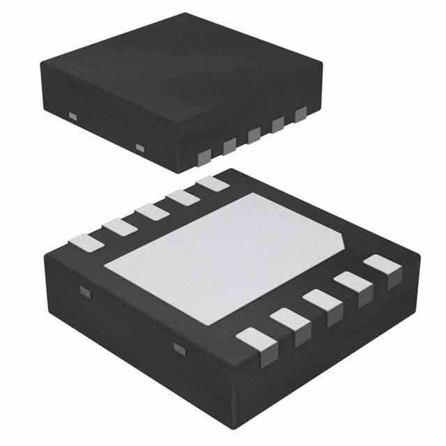
WSON-10 Package (3mm × 3mm × 0.8mm)
APPLICATIONS
•
•
•
The LM2772 utilizes a highly efficient regulated multigain charge pump. Pre-regulated 1.1MHz fixedfrequency switching results in very low ripple and
noise on both the input and the output. When output
currents are low, the part automatically switches to a
low-ripple PFM regulation mode to maintain high
efficiency over the entire load range.
The LM2772 is available in TI’s WSON-10 Package
(WSON-10).
DSP, Memory, and Microprocessor Power
Supplies
Mobile Phones and Pagers
Portable Electronic Devices
Typical Application Circuit
VOUT: 1.2V
VIN = 3.0V to 5.5V
IOUT up to 150 mA
VIN
VOUT
CIN
COUT
1 µF
4.7 µF
C1+
GND
LM2772
C1
1 µF
High: ON
Low: Shutdown
C1C2+
EN
C3+
C3
1 µF
C2
1 µF
C3-
C2-
Capacitors: 1 µF - TDK C1005X5R0J105K
4.7 µF - TDK C1608X5R0J475K
or equivalent
Figure 1.
Figure 2. LM2772 Efficiency vs.
Low-Dropout Linear Regulator (LDO) Efficiency
1
2
Please be aware that an important notice concerning availability, standard warranty, and use in critical applications of
Texas Instruments semiconductor products and disclaimers thereto appears at the end of this data sheet.
All trademarks are the property of their respective owners.
PRODUCTION DATA information is current as of publication date.
Products conform to specifications per the terms of the Texas
Instruments standard warranty. Production processing does not
necessarily include testing of all parameters.
Copyright © 2006–2013, Texas Instruments Incorporated
�LM2772
SNVS486B – DECEMBER 2006 – REVISED MAY 2013
www.ti.com
Connection Diagram
VIN
1
10
EN
EN
10
1
VIN
GND
2
9
C1+
C1+
9
2
GND
VOUT
3
8
C1-
C1-
8
3
VOUT
C3-
4
7
C2+
C2+
7
4
C3-
C3+
5
6
C2-
C2-
6
5
C3+
Die-Attach Pad: GND
Die-Attach Pad: GND
Top View
Bottom View
10-Pin WSON Package (WSON-10)
See Package Number DSC0010A
PIN DESCRIPTIONS
Pin #
Name
1
VIN
Description
2
GND
Ground
3
VOUT
Output Voltage
4
C3-
Flying Capacitor 3: Negative Terminal
5
C3+
Flying Capacitor 3: Positive Terminal
6
C2-
Flying Capacitor 2: Negative Terminal
7
C2+
Flying Capacitor 2: Positive Terminal
8
C1-
Flying Capacitor 1: Negative Terminal
9
C1+
Flying Capacitor 1: Positive Terminal
10
EN
Enable Pin Logic Input. Applying a logic HIGH voltage signal enables the part. A logic LOW
voltage signal places the the device in shutdown.
Input Voltage: Recommended VIN operating range 3.0V to 5.5V.
These devices have limited built-in ESD protection. The leads should be shorted together or the device placed in conductive foam
during storage or handling to prevent electrostatic damage to the MOS gates.
2
Submit Documentation Feedback
Copyright © 2006–2013, Texas Instruments Incorporated
Product Folder Links: LM2772
�LM2772
www.ti.com
SNVS486B – DECEMBER 2006 – REVISED MAY 2013
Absolute Maximum Ratings (1) (2) (3)
VIN Pin Voltage
-0.3V to 6.0V
EN Pin Voltage
-0.3V to (VIN+0.3V) w/ 6.0V max
Continuous Power Dissipation (4)
Internally Limited
Junction Temperature (TJ-MAX)
150ºC
Storage Temperature Range
Maximum Lead Temperature
-65ºC to +150º C
(5)
265ºC
ESD Rating (6)
Human Body Model:
(1)
(2)
(3)
(4)
(5)
(6)
2.0kV
Absolute Maximum Ratings indicate limits beyond which damage to the component may occur. Operating Ratings are conditions under
which operation of the device is ensured. Operating Ratings do not imply ensured performance limits. For ensured performance limits
and associated test conditions, see the Electrical Characteristics tables.
If Military/Aerospace specified devices are required, please contact the TI Sales Office/Distributors for availability and specifications.
All voltages are with respect to the potential at the GND pins.
Internal thermal shutdown circuitry protects the device from permanent damage. Thermal shutdown engages at TJ=150ºC (typ.) and
disengages at TJ=140ºC (typ.).
For detailed information on soldering requirements and recommendations, please refer to Texas Instruments' Application Note 1187
(SNOA401): Leadless Leadframe Package (LLP).
The Human body model is a 100pF capacitor discharged through a 1.5kΩ resistor into each pin. MIL-STD-883 3015.7
Operating Ratings (1) (2)
Input Voltage Range
2.7V to 5.5V
Recommended Load Current Range
0mA to 150mA
Junction Temperature (TJ) Range
-30°C to +110°C
Ambient Temperature (TA) Range (3)
(1)
(2)
(3)
-30°C to +85°C
Absolute Maximum Ratings indicate limits beyond which damage to the component may occur. Operating Ratings are conditions under
which operation of the device is ensured. Operating Ratings do not imply ensured performance limits. For ensured performance limits
and associated test conditions, see the Electrical Characteristics tables.
All voltages are with respect to the potential at the GND pins.
Maximum ambient temperature (TA-MAX) is dependent on the maximum operating junction temperature (TJ-MAX-OP = 110ºC), the
maximum power dissipation of the device in the application (PD-MAX), and the junction-to ambient thermal resistance of the part/package
in the application (θJA), as given by the following equation: TA-MAX = TJ-MAX-OP – (θJA × PD-MAX).
Thermal Properties
Junction-to-Ambient Thermal
Resistance (θJA), WSON-10 Package (1)
(1)
55°C/W
Junction-to-ambient thermal resistance is highly application and board-layout dependent. In applications where high maximum power
dissipation exists, special care must be paid to thermal dissipation issues.
Submit Documentation Feedback
Copyright © 2006–2013, Texas Instruments Incorporated
Product Folder Links: LM2772
3
�LM2772
SNVS486B – DECEMBER 2006 – REVISED MAY 2013
www.ti.com
Electrical Characteristics (1) (2)
Limits in standard typeface are for TJ = 25ºC. Limits in boldface type apply over the full operating junction temperature range
(-30°C ≤ TJ ≤ +110°C) . Unless otherwise noted, specifications apply to the LM2772 Typical Application Circuit (pg. 1) with:
VIN = 3.6V; V(EN) = 1.8V, CIN = C1 = C2 = C3 = 1.0µF, COUT = 4.7µF. (3)
Symbol
VOUT
Parameter
1.2V Output Voltage Regulation
Typ
Max
3.0V ≤ VIN ≤ 5.5V
0mA ≤ IOUT ≤ 150mA
Condition
1.164
(−3%)
Min
1.2
1.236
(+3%)
0mA ≤ IOUT ≤ 150mA
1.178
(−1.8%)
1.2
1.236
(+3.0%)
0mA ≤ IOUT ≤ 150mA
Units
V
VOUT/IOUT
Output Load Regulation
VOUT/VIN
Output Line Regulation
E
Power Efficiency
IOUT = 150mA
80
IQ
Quiescent Supply Current
IOUT = 0mA (4)
47
VR
Fixed Frequency Output Ripple
40mA ≤ IOUT ≤ 150mA
8
VR–PFM
PFM–Mode Output Ripple
IOUT < 40mA
12
ISD
Shutdown Current
V(EN) = 0V
0.01
0.3
µA
FSW
Switching Frequency
3.0V ≤ VIN ≤ 5.5V
1.15
1.50
MHz
ICL
Output Current Limit
VIN = 5.5V
0V ≤ VOUT ≤ 0.2V
tON
Turn-on Time
VIL
Logic-low Input Voltage
3.0V ≤ VIN ≤ 5.5V
0
VIH
Logic-high Input Voltage
3.0V ≤ VIN ≤ 5.5V
1.1
IIH
Logic-high Input Current
V(EN) = 1.8V (5)
5
µA
IIL
Logic-low Input Current
Logic Input = 0V
0.01
µA
(1)
(2)
(3)
(4)
(5)
4
0.80
0.15
mV/mA
0.2
%/V
%
50
µA
mV
mV
500
mA
150
µs
0.63
VIN
V
V
All voltages are with respect to the potential at the GND pins.
Min and Max limits are specified by design, test, or statistical analysis. Typical numbers are not ensured, but do represent the most
likely norm.
CIN, COUT, C1, C2, C3: Low-ESR Surface-Mount Ceramic Capacitors (MLCCs) used in setting electrical characteristics.
VOUT is set to 1.3V during this test (Device is not switching).
There is a 350kΩ pull-down resistor connected internally between the EN pin and GND.
Submit Documentation Feedback
Copyright © 2006–2013, Texas Instruments Incorporated
Product Folder Links: LM2772
�LM2772
www.ti.com
SNVS486B – DECEMBER 2006 – REVISED MAY 2013
BLOCK DIAGRAM
LM2772
VIN
C1+
C11.04M
SWITCH
ARRAY
GAIN
CONTROL
950k
SWITCH
CONTROL
1
2
C2+
1
G =2, 5,3
C2C3+
C3-
775k
PFM
Control
GND
VOUT
Current
sense
1.1 MHz
OSC.
1.25V
Ref.
EN
Enable/
Shutdown
Control
EN
Soft-Start
Ramp
0.8V
Ref.
Submit Documentation Feedback
Copyright © 2006–2013, Texas Instruments Incorporated
Product Folder Links: LM2772
5
�LM2772
SNVS486B – DECEMBER 2006 – REVISED MAY 2013
www.ti.com
Typical Performance Characteristics
Unless otherwise specified: VIN = 3.6V, CIN = C1 = C2 = C3 = 1.0µF, COUT = 4.7µF, TA = 25ºC. Capacitors are low-ESR multilayer ceramic capacitors (MLCC's).
Output Voltage
vs.
Input Voltage
Output Voltage
vs.
Output Current
Figure 3.
Figure 4.
Efficiency
vs.
Input Voltage
Operating Supply Current
Figure 5.
Figure 6.
Input and Output Voltage Ripple, Load = 150mA
Load Step 10mA to 150mA, VIN = 3.6V
CH1: VIN, Scale: 50mV/Div, AC Coupled
CH3: VOUT, Scale: 10mV/Div, AC Coupled
Time scale: 1µs/Div
Figure 7.
6
Submit Documentation Feedback
CH3: VOUT; Scale: 50mV/Div, AC Coupled
CH4: IOUT; Scale: 100mA/Div
Time scale: 40µs/Div
Figure 8.
Copyright © 2006–2013, Texas Instruments Incorporated
Product Folder Links: LM2772
�LM2772
www.ti.com
SNVS486B – DECEMBER 2006 – REVISED MAY 2013
Typical Performance Characteristics (continued)
Unless otherwise specified: VIN = 3.6V, CIN = C1 = C2 = C3 = 1.0µF, COUT = 4.7µF, TA = 25ºC. Capacitors are low-ESR multilayer ceramic capacitors (MLCC's).
Load Step 10mA to 150mA, VIN = 4.7V
CH3: VOUT; Scale: 50mV/Div, AC Coupled
CH4: IOUT; Scale: 100mA/Div
Time scale: 40µs/Div
Figure 9.
Line Step 3.5V to 4.0V with Load = 150mA
CH2: VIN; Scale: 1V/Div, DC Coupled
CH3: VOUT; Scale: 20mV/Div, AC Coupled
Time scale: 400µs/Div
Figure 10.
Line Step 4.0V to 3.5V with Load = 150mA
CH2: VIN; Scale: 1V/Div, DC Coupled
CH3: VOUT; Scale: 20mV/Div, AC Coupled
Time scale: 400µs/Div
Figure 11.
Oscillator Frequency
vs.
Input Voltage
Figure 12.
Startup Behavior, Load = 150mA
CH1: VOUT; Scale: 200mV/Div, DC Coupled
Time scale: 20µs/Div
Figure 13.
Submit Documentation Feedback
Copyright © 2006–2013, Texas Instruments Incorporated
Product Folder Links: LM2772
7
�LM2772
SNVS486B – DECEMBER 2006 – REVISED MAY 2013
www.ti.com
OPERATION DESCRIPTION
Overview
The LM2772 is a switched capacitor converter that produces a regulated, low voltage output. The core of the part
is a highly efficient charge pump that utilizes fixed frequency pre-regulation and Pulse Frequency Modulation to
minimize ripple and power losses over wide input voltage and output current ranges. A description of the
principal operational characteristics of the LM2772 is detailed in the Circuit Description, and Efficiency
Performance sections. These sections refer to details in the Block Diagram.
Circuit Description
The core of the LM2772 is a two-phase charge pump controlled by an internally generated non-overlapping
clock. The charge pump operates by using external flying capacitors C1, C2, and C3 to transfer charge from the
input to the output. At input voltages below 3.5V (typ.) the LM2772 operates in a 1/2x Gain, with the input current
being equal to 1/2 of the load current. At input voltages between 3.5V to 4.6V(typ.) the part utilizes a gain of 2/5x,
resulting in an input current equal to 2/5 times the load current. At input voltages above 4.6V (typ.), the part is in
a gain of 1/3, with the input current being 1/3 of the load current.
The two phases of the switched capacitor switching cycle will be referred to as the "charge phase" and the
"discharge phase". During the charge phase, the flying capacitor is charged by the input supply. After half of the
switching cycle [ t = 1/(2×FSW) ], the LM2772 switches to the discharge phase. In this configuration, the charge
that was stored on the flying capacitors in the charge phase is transferred to the output.
The LM2772 uses fixed frequency pre-regulation to regulate the output voltage to 1.2V during moderate to high
load currents. The input and output connections of the flying capacitors are made with internal MOS switches.
Pre-regulation limits the gate drive of the MOS switch connected between the voltage input and the flying
capacitors. Controlling the on resistance of this switch limits the amount of charge transferred into and out of
each flying capacitor during the charge and discharge phases, and in turn helps to keep the output ripple very
low.
When output currents are low (


 工商网监
湘ICP备2023018690号
工商网监
湘ICP备2023018690号
