LM2793
LM2793 Low Noise White LED Constant Current Supply with Dual Function
Brightness Control
Literature Number: SNVS228
�LM2793
Low Noise White LED Constant Current Supply with
Dual Function Brightness Control
General Description
Features
The LM2793 is a highly efficient, semi-regulated 1.5x CMOS
charge pump that provides dual constant current outputs.
The LM2793 has an input voltage range of 2.7V to 5.5V.
n Two Regulated Current Outputs, up to 16mA Each,
Matched to Within ± 0.3% (typ.)
n High Efficiency, 1.5x Regulated Charge Pump
n Input Voltage Range: 2.7V to 5.5V
n Soft Start Limits Inrush Current
n Analog Voltage Brightness Control
n PWM Brightness Control
n Very Small Solution Size - NO INDUCTOR
n 500kHz Switching Frequency
n 3µA (typ.) Shutdown Current
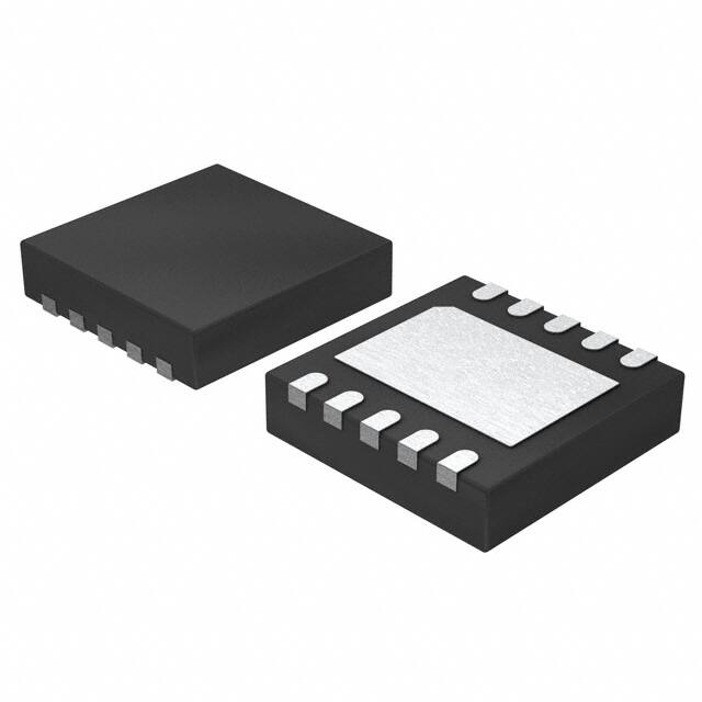
n LLP-10 Package: 3.0mm X 3.0mm X 0.8mm
To control LED brightness, the amount of current driven to
the current-mode outputs can be adjusted with an analog
voltage and/or a pulse-width-modulated (PWM) square
wave.
Pre-regulation of the charge pump minimizes conducted
noise on the input. Combined with a fixed switching frequency of 500kHz, the LM2793 is a low-noise solution.
The LM2793 is available in a 10-pin Leadless Lead-frame
package: LLP-10.
Applications
n White LED Display Backlights
n White LED Keypad Backlights
n 1-Cell LiIon Battery-Operated Equipment Including
PDAs, Hand-held PCs, Cellular Phones
n Flat Panel Displays
Typical Application Circuit
20063602
© 2003 National Semiconductor Corporation
DS200636
www.national.com
LM2793 Low Noise White LED Constant Current Supply with Dual Function Brightness Control
February 2003
�LM2793
Connection Diagram
LM2793
10-pin Leadless Leadframe Package (LLP-10)
3mmx3mmx0.8mm
NS Package Number LDA10A
20063603
Top View
Ordering Information
Order Number
Package Description
Package
Marking
Supplied as Tape and Reel
(Units)
LM2793LD
LLP-10
LM2793
1000
LM2793LDX
LLP-10
LM2793
4500
Pin Description
Pin
Name
1
VIN
Description
Power supply voltage connection
2
C1-
Flying capacitor C1 connection
3
C2+
Flying capacitor C2 connection
4
C1+
Flying capacitor C1 connection
5
POUT
Charge pump output
6
D1
7
D2
8
SD-BRGT
9
GND
10
C2-
www.national.com
Current source output / LED connection
Current source output / LED connection
Dual function Shutdown - Brightness. Grounding pin shuts down part. Voltage
between 0.75V and 2.75V (typ.) linearly adjusts current outputs. Output current
equals 16mA at voltages above 2.75V.
Power supply ground connection
Flying capacitor C2 connection
2
�Operating Ratings (Notes 2, 8)
(Notes 1,
2)
Input Voltage VIN
If Military/Aerospace specified devices are required,
please contact the National Semiconductor Sales Office/
Distributors for availability and specifications.
VSD-BRGT
Continuous Power Dissipation (Note
4)
0V to VIN
Brightness Adjustment Control
Range of VSD-BRGT
0.75V to 2.75V
-0.3V to 6.0V
Junction Temperature Range (TJ)
-30˚C to +100˚C
-0.3V to (VIN +
0.3V) w/ 6.0V max
Ambient Temperature Range (TA)
-30˚C to +85 ˚C
(Note 6)
Internally Limited
Thermal Information
VIN
VSD-BRGT
2.7V to 5.5V
Junction Temperature (TJ-MAX-ABS)
150˚C
Storage Temperature Range
Junction-to-Ambient Thermal
Resistance,
LLP-10 Package (θJA) (Note 7)
-65˚C to 150˚C
Lead Temp. (Soldering, 5 sec.)
260˚C
ESD Rating (Note 5)
Human Body Model
55˚C/W
2kV
Machine Model
200V
Electrical Characteristics
(Notes 2, 8)
Limits in standard typeface are for TJ = 25˚C, and limits in boldface type apply over the full operating junction temprature
range. Unless otherwise specified: C1=C2=CIN=CHOLD=1µF; VIN=3.6V; VSD-BRGT=3.0V; VDX=3.6V
Symbol
IDX
Parameter
Output Current Regulation
ID-MATCH
ID1-to-ID2 Current Matching
ROUT
Charge Pump Output
Resistance
VHR-min
IQ
Conditions
Min
Typ
Max
3.3V ≤ VIN ≤ 5.5V
VDX = 3.9V
14.7
13.7
15.9
17.2
17.3
3.0V ≤ VIN ≤ 5.5V
VDX = 3.8V
14.7
13.7
15.9
17.2
17.3
2.7V ≤ VIN ≤ 5.5V
VDX = 3.4V
14.7
13.7
15.9
17.2
17.3
2.5V ≤ VDX ≤ 3.9V
(Note 9)
14.7
13.7
15.9
17.2
17.3
VSD-BRGT= 2.0V
10
VSD-BRGT= 0.75V
0.1
0.3
3.0
Units
mA
%
3.5
Ω
Minimum Current Source
Voltage Headroom (VPOUT - IDX = 16mA
VIDx) (Note 10)
400
mV
Quiescent Supply Current
IDX, IPOUT = 0
1.2
2.2
mA
ISD
Shutdown Supply Current
2.7V ≤ VIN ≤ 5.5V
VSD-BRGT = 0V
3
5
µA
ON/OFF
SD-BRGT Pin Thresholds
for Active and Shutdown
Modes
ILEAK-SD
SD-BRGT Pin Leakage
Current
fSW
Switching Frequency
2.7V ≤ VIN ≤ 5.5V
tSTART
Startup Time
IDX = 90% steady state
VIN = 2.7V
Active
VIN = 3.0V
0.70
0.25
Shutdown
VIN = 3.0V
17
325
500
30
V
µA
675
kHz
µs
Note 1: Absolute Maximum Ratings indicate limits beyond which damage to the component may occur. Operating Ratings are conditions under which operation of
the device is guaranteed. Operating Ratings do not imply guaranteed performance limits. For guaranteed performance limits and associated test conditions, see the
Electrical Characteristics tables.
Note 2: All voltages are with respect to the potential at the GND pin.
Note 3: Voltage on the SD-BRGT pin should not exceed 6V.
Note 4: Thermal shutdown circuitry protects the device from permanent damage. D1 and D2 may be shorted to GND without damage.
3
www.national.com
LM2793
Absolute Maximum Ratings
�LM2793
Electrical Characteristics
(Notes 2, 8) (Continued)
Note 5: The human-body model is a 100 pF capacitor discharged through a 1.5 k resistor into each pin. The machine model is a 200pF capacitor discharged directly
into each pin.
Note 6: Maximum ambient temperature (TA-MAX) is dependent on the maximum operating junction temperature (TJ-MAX-OP = 100oC), the maximum power
dissipation of the device in the application (PD-MAX), and the junction-to-ambient thermal resistance of the part/package in the application (θJA), as given by the
following equation: TA-MAX = TJ-MAX-OP - (θJA x PD-MAX). The ambient temperature operating rating is provided merely for convenience. This part may be operated
outside the listed TA rating, so long as the junction temperature of the device does not exceed the maximum operating rating of 100oC.
Note 7: Junction-to-ambient thermal resistance is highly application and board-layout dependent. In applications where high maximum power dissipation exists,
special care must be paid to thermal dissipation issues. For more information on these topics, please refer to the Power Dissipation section of this datasheet.
Note 8: All room temperature limits are 100% tested or guaranteed through statistical analysis. All limits at temperature extremes are guaranteed by correlation
using standard Statistical Quality Control methods (SQC). All limits are used to calculate Average Outgoing Quality Level (AOQL). Typical numbers are not
guaranteed, but do represent the most likely norm.
Note 9: Maximum LED voltage (VDx) is highly dependent on the application’s minimum input voltage and the amount of current flowing through the LEDs. Maximum
LED voltage for a given application can be approximated with the following equations:
VIN-MIN < 3.0V: VDx-MAX = (1.5 x VIN-MIN) - (IDXx 25 mV/mA) - (3.5Ω x 2 x IDX)
VIN-MIN ≥ 3.0V: VDx-MAX = 4.3V - (IDX x 25 mV/mA)
The equations above assume LEDs are connected to outputs D1 and D2, and no current drawn from the charge pump output (POUT). For a more precise and
thorough analysis of maximum LED voltage, please refer to text sections of the datasheet (to appear in future datasheet revisions - in the interim, please contact
National Semiconductor for more information).
Note 10: Current sources are connected internally between POUT and IDx. The voltage across each current source, [V(POUT) - V(IDx)], is referred to as headroom
voltage. For current sources to regulate properly, a minimum headroom voltage must be present across them. Minimum required headroom voltage is proportional
to the current flowing through the current source, as dictated by this equation: VHR-min = 400mV x (IDx / 16mA).
Block Diagram
20063601
www.national.com
4
�LED Current vs. Input Voltage
LED Current vs. SD-BRGT Voltage
20063606
20063607
Efficiency vs. Input Voltage
LED Current vs. LED Voltage
20063612
20063608
Quiescent Current vs. Input Voltage
Shutdown Supply Current vs. Input Voltage
20063609
20063610
5
www.national.com
LM2793
Typical Performance Characteristics Unless otherwise specified: TA = 25˚C, 2 LEDs, VDX = 3.6V,
VIN = 3.6, VSD-BRGT = 3.0, C1 = C2 = CIN = CHOLD = 1µF. Capacitors are low-ESR multi-layer ceramic capacitors (MLCC’s).
�LM2793
Typical Performance Characteristics Unless otherwise specified: TA = 25˚C, 2 LEDs, VDX = 3.6V,
VIN = 3.6, VSD-BRGT = 3.0, C1 = C2 = CIN = CHOLD = 1µF. Capacitors are low-ESR multi-layer ceramic capacitors
(MLCC’s). (Continued)
Output Resistance vs. Temperature
Startup Response
20063614
20063611
www.national.com
6
�LM2793
Application Information
CIRCUIT DESCRIPTION
The LM2793 is a 1.5x CMOS charge pump that provides two
matched constant current outputs for driving up to 16mA
through high forward voltage drop White LEDs from Li-Ion
battery sources. The device has two regulated current
sources connected to the output of the device’s 1.5x loosely
regulated charge pump (POUT). The device’s looselyregulated charge pump has both open loop and closed loop
modes of operation. When the device is in open loop, the
voltage at POUT is 1.5 times the voltage at the input. When
the device is in closed loop, the voltage at POUT is loosely
regulated to 4.9V (typ.). To set the LED drive current, the
device uses the voltage applied to the dual function
shutdown-brightness pin (SD-BRGT) to set a reference current. This reference current is then multiplied and mirrored to
each current output. The LED brightness can be controlled
by both analog and/or digital methods. The digital technique
uses a PWM (Pulse Width Modulation) signal applied to the
SD-BRGT pin. The analog technique applies an analog voltage in the range of 0.7V to 2.75 to the SD-BRGT pin to vary
the LED current (see Shutdown and Brightness Control).
20063607
FIGURE 1. LED Current vs. VSD-BRGT
2 LEDs, VDX = 3.6V, VIN = 3.6V
CAPACITOR SELECTION
The LM2793 requires 4 external capacitors for proper operation. Surface-mount multi-layer ceramic capacitors are recommended. These capacitors are small, inexpensive and
have very low equivalent series resistance (ESR, ≤15mΩ
typ.). Tantalum capacitors, OS-CON capacitors, and aluminum electrolytic capacitors are generally not recommended
for use with the LM2793 due to their high ESR, as compared
to ceramic capacitors.
For most applications, ceramic capacitors with X7R or X5R
temperature characteristic are preferred for use with the
LM2793. These capacitors have tight capacitance tolerance
(as good as ± 10%), hold their value over temperature (X7R:
± 15% over −55˚C to 125˚C; X5R: ± 15% over −55˚C to
85˚C), and typically have little voltage coefficient. Capacitors
with Y5V or Z5U temperature characteristic are generally not
recommended for use with the LM2793. Capacitors with
these temperature characteristics typically have wide capacitance tolerance (+80%, −20%), vary significantly over
temperature (Y5V: +22%, −82% over −30˚C to +85˚C range;
Z5U: +22%, −56% over +10˚C to +85˚C range), and have
poor voltage coefficients. Under some conditions, a nominal
1µF Y5V or Z5U capacitor could have a capacitance of only
0.1µF. Such detrimental deviation is likely to cause Y5V and
Z5U capacitors to fail to meet the minimum capacitance
requirements of the LM2793. Table 1 lists suggested capacitor suppliers for the typical application circuit.
SOFT START
LM2793 includes a soft start function to reduce the inrush
currents and high peak current during power up of the device. Soft start is implemented internally by ramping the
reference voltage more slowly than the applied voltage.
During soft start, the switch resistances limit the inrush current used to charge the flying and hold capacitors.
SHUTDOWN AND BRIGHTNESS CONTROL
The LM2793 has an active-low dual function shutdownbrightness control pin, SD-BRGT. A voltage higher than
0.65V (typ.) on SD-BRGT will put the LM2793 in active
mode. Applying a voltage below 0.35V (typ.) on the SDBRGT pin will turn off the device, reducing the quiescent
current to 3µA (typ.).
The LM2793 has the ability to adjust LED brightness by
applying an analog voltage or a PWM signal to the SDBRGT pin. For constant brightness or analog brightness
control, continue with “Analog brightness control” below.
Otherwise go to “Brightness control using PWM”.
1. Analog brightness control
The current for the dual LED outputs can be adjusted by
varying the voltage on the SD-BRGT pin. The typical
range for adjusting LED brightness is between 0.7 and
2.75V. Figure 1 shows how the current changes with
respect to the voltage applied to SD-BRGT. If full brightness (16mA) is desired, the voltage on SD-BRGT should
be greater than 2.75V (typ.) but not more than VIN.
2.
TABLE 1. Ceramic Capacitor Manufacturers
Brightness control using PWM
Increasing and decreasing the duty cycle of the PWM
signal controls the LED brightness. Zero duty cycle will
turn off the LEDs and a 50% duty cycle will result in an
average ILED being half of the maximum LED current.
The recommended frequency range for the PWM signal
is between 100Hz and 1KHz. If the PWM frequency is
much less than 100Hz, flicker may be seen in the LEDs.
If the frequency is much higher than 1kHz, brightness in
the LEDs will not adjust linearly with duty cycle due to
the 30µs (typ.) start-up time of the device. The voltage
level for the PWM signal should be greater than 2.75V
(typ.) but not exceed the voltage on VIN.
Manufacturer
Contact
TDK
www.component.tdk.com
Murata
www.murata.com
Taiyo Yuden
www.t-yuden.com
LED SELECTION
The LM2793 is designed to drive LEDs with a forward voltage of about 3.0V to 4.0V. The typical and maximum diode
forward voltage depends highly on the manufacturer and
their technology. Table 2 lists two suggested manufacturers.
Forward current matching is assured over the LED process
variations due to the constant current output of the LM2793.
7
www.national.com
�LM2793
Application Information
through one LED, and VLED is the forward voltage at that
LED current. In the input power calculation, the 1.5 multiplier
reflects the 3/2 switched capacitor gain of the LM2793.
PLED = N x VLED x ILED
PIN = VIN x IIN
(Continued)
TABLE 2. White LED Selection
Manufacturer
Contact
Osram
www.osram-os.com
Nichia
www.nichia.com
PIN = VIN x (1.5 x N x ILED + IQ)
E = (PLED ÷ PIN)
It is also worth noting that efficiency as defined here is in part
dependent on LED voltage. Variation in LED voltage does
not affect power consumed by the circuit and typically does
not relate to the brightness of the LED. For an advanced
analysis, it is recommended that power consumed by the
circuit (VIN x IIN) be evaluated rather than power efficiency.
Power consumption of the LM2793 Typical Application Circuit is shown in Figure 3.
PARALLEL DX OUTPUTS FOR INCREASED CURRENT
DRIVE
Outputs D1 and D2 may be connected together to drive a
single LED. In such a configuration, two parallel current
sources of equal value drive the single LED. The voltage on
SD-BRGT should be chosen so that the current through
each of the outputs is programmed to 50% of the total
desired LED current. For example, if 30mA is the desired
drive current for the single LED, SD-BRGT should be selected so that the current through each of the outputs is
15mA. Connecting the outputs in parallel does not affect
internal operation of the LM2793 and has no impact on the
Electrical Characteristics and limits previously presented.
The available diode output current, maximum diode voltage,
and all other specifications provided in the Electrical Characteristics table apply to this parallel output configuration,
just as they do to the standard 2-LED application circuit.
POUT
POUT uses pre-regulation to loosely regulate the output of
the LM2793 1.5x charge pump. Pre-regulation uses the
voltage present at POUT to limit the gate drive of the 1.5x
switched capacitor charge pump. Pre-regulation helps to
reduce input current noise and large input current spikes
normally associated with switched capacitor charge pumps.
At voltages below 3.3V (typ.), the LM2793 acts as an open
loop charge pump. When the device is in open loop, the
voltage at POUT is 1.5 times the input voltage. At input
voltages higher than 3.3V (typ.) POUT is loosely regulated to
4.9V (typ.).
20063613
FIGURE 3. ILED current vs. PIN
2 LEDs, 2.5 ≤ VLED ≤ 3.9V, ILED = 16mA
THERMAL PROTECTION
When the junction temperature exceeds 150˚C, the LM2793
internal thermal protection circuitry disables the part. This
feature protects the device from damage due to excessive
power dissipation. The device will recover and operate normally when the junction temperature falls below 125˚C. It is
important to have good thermal conduction with a proper
layout to reduce thermal resistance.
POWER EFFICIENCY
Figure 2 shows the efficiency of the LM2793.
POWER DISSIPATION
When operating within specified operating ratings, the peak
power dissipation (PDISSIPATION) of the LM2793 occurs at an
input voltage of 5.5V. Assuming a typical junction-to-ambient
thermal resistance (θJA) for the LLP-10 package of 55˚C/W,
a LED forward voltage (VDX) of 3.6V, and a total load (ILOAD)
of 32mA for two White LEDs connected to D1 and D2, the
power dissipation and junction temperature (TJ) are calculated below for a part operating at the maximum rated ambient temperature (TA) of 85˚C. In the equations below, VIN is
the input voltage to the LM2793, PIN is the power generated
by the 1.5x charge pump, and PLED is the power consumed
by the LEDs.
PDISSIPATION = PIN - PLED
= (1.5VIN − VDX) x ILOAD
= ((1.5 x 5.5V) - 3.6V) x 0.032A
= 149mW
20063612
FIGURE 2. Efficiency vs. VIN
2 LEDs, VLED = 3.6V, ILED = 16mA
Efficiency (E) of the LM2793 is defined here as the ratio of
the power consumed by LEDs (PLED) to the power drawn
from the input source (PIN). In the equations below, IQ is the
quiescent current of the LM2793, ILED is the current flowing
www.national.com
8
�measuring 2.0mm x 1.2mm. The main advantage of this
exposed DAP is to offer lower thermal resistance when it is
soldered to the thermal land on the PCB. For PCB layout,
National highly recommends a 1:1 ratio between the package and the PCB thermal land. To further enhance thermal
conductivity, the PCB thermal land may include vias to a
ground plane. For more detailed instructions on mounting
LLP packages, please refer to National Semiconductor Application Note AN-1187.
(Continued)
TJ = TA + (PDMAX x θJA)
= 85˚C + (0.149W x 55˚C/W)
= 93˚C
The junction temperature rating takes precedence over the
ambient temperature rating. The LM2793 may be operated
outside the ambient temperature rating, so long as the junction temperature of the device does not exceed the maximum operating rating of 100˚C. The maximum ambient temperature rating must be derated in applications where high
power dissipation and/or poor thermal resistance causes the
junction temperature to exceed 100˚C.
PCB Layout Considerations
The LLP is a leadframe based Chip Scale Package (CSP)
with very good thermal properties. This package has an
exposed DAP (die attach pad) at the center of the package
9
www.national.com
LM2793
Application Information
�LM2793 Low Noise White LED Constant Current Supply with Dual Function Brightness Control
Physical Dimensions
inches (millimeters) unless otherwise noted
10-Pin LLP
NS Package Number LDA10A
LIFE SUPPORT POLICY
NATIONAL’S PRODUCTS ARE NOT AUTHORIZED FOR USE AS CRITICAL COMPONENTS IN LIFE SUPPORT
DEVICES OR SYSTEMS WITHOUT THE EXPRESS WRITTEN APPROVAL OF THE PRESIDENT AND GENERAL
COUNSEL OF NATIONAL SEMICONDUCTOR CORPORATION. As used herein:
1. Life support devices or systems are devices or
systems which, (a) are intended for surgical implant
into the body, or (b) support or sustain life, and
whose failure to perform when properly used in
accordance with instructions for use provided in the
labeling, can be reasonably expected to result in a
significant injury to the user.
National Semiconductor
Americas Customer
Support Center
Email: new.feedback@nsc.com
Tel: 1-800-272-9959
www.national.com
National Semiconductor
Europe Customer Support Center
Fax: +49 (0) 180-530 85 86
Email: europe.support@nsc.com
Deutsch Tel: +49 (0) 69 9508 6208
English Tel: +44 (0) 870 24 0 2171
Français Tel: +33 (0) 1 41 91 8790
2. A critical component is any component of a life
support device or system whose failure to perform
can be reasonably expected to cause the failure of
the life support device or system, or to affect its
safety or effectiveness.
National Semiconductor
Asia Pacific Customer
Support Center
Fax: +65-6250 4466
Email: ap.support@nsc.com
Tel: +65-6254 4466
National Semiconductor
Japan Customer Support Center
Fax: 81-3-5639-7507
Email: jpn.feedback@nsc.com
Tel: 81-3-5639-7560
National does not assume any responsibility for use of any circuitry described, no circuit patent licenses are implied and National reserves the right at any time without notice to change said circuitry and specifications.
�IMPORTANT NOTICE
Texas Instruments Incorporated and its subsidiaries (TI) reserve the right to make corrections, modifications, enhancements, improvements,
and other changes to its products and services at any time and to discontinue any product or service without notice. Customers should
obtain the latest relevant information before placing orders and should verify that such information is current and complete. All products are
sold subject to TI’s terms and conditions of sale supplied at the time of order acknowledgment.
TI warrants performance of its hardware products to the specifications applicable at the time of sale in accordance with TI’s standard
warranty. Testing and other quality control techniques are used to the extent TI deems necessary to support this warranty. Except where
mandated by government requirements, testing of all parameters of each product is not necessarily performed.
TI assumes no liability for applications assistance or customer product design. Customers are responsible for their products and
applications using TI components. To minimize the risks associated with customer products and applications, customers should provide
adequate design and operating safeguards.
TI does not warrant or represent that any license, either express or implied, is granted under any TI patent right, copyright, mask work right,
or other TI intellectual property right relating to any combination, machine, or process in which TI products or services are used. Information
published by TI regarding third-party products or services does not constitute a license from TI to use such products or services or a
warranty or endorsement thereof. Use of such information may require a license from a third party under the patents or other intellectual
property of the third party, or a license from TI under the patents or other intellectual property of TI.
Reproduction of TI information in TI data books or data sheets is permissible only if reproduction is without alteration and is accompanied
by all associated warranties, conditions, limitations, and notices. Reproduction of this information with alteration is an unfair and deceptive
business practice. TI is not responsible or liable for such altered documentation. Information of third parties may be subject to additional
restrictions.
Resale of TI products or services with statements different from or beyond the parameters stated by TI for that product or service voids all
express and any implied warranties for the associated TI product or service and is an unfair and deceptive business practice. TI is not
responsible or liable for any such statements.
TI products are not authorized for use in safety-critical applications (such as life support) where a failure of the TI product would reasonably
be expected to cause severe personal injury or death, unless officers of the parties have executed an agreement specifically governing
such use. Buyers represent that they have all necessary expertise in the safety and regulatory ramifications of their applications, and
acknowledge and agree that they are solely responsible for all legal, regulatory and safety-related requirements concerning their products
and any use of TI products in such safety-critical applications, notwithstanding any applications-related information or support that may be
provided by TI. Further, Buyers must fully indemnify TI and its representatives against any damages arising out of the use of TI products in
such safety-critical applications.
TI products are neither designed nor intended for use in military/aerospace applications or environments unless the TI products are
specifically designated by TI as military-grade or "enhanced plastic." Only products designated by TI as military-grade meet military
specifications. Buyers acknowledge and agree that any such use of TI products which TI has not designated as military-grade is solely at
the Buyer's risk, and that they are solely responsible for compliance with all legal and regulatory requirements in connection with such use.
TI products are neither designed nor intended for use in automotive applications or environments unless the specific TI products are
designated by TI as compliant with ISO/TS 16949 requirements. Buyers acknowledge and agree that, if they use any non-designated
products in automotive applications, TI will not be responsible for any failure to meet such requirements.
Following are URLs where you can obtain information on other Texas Instruments products and application solutions:
Products
Applications
Audio
www.ti.com/audio
Communications and Telecom www.ti.com/communications
Amplifiers
amplifier.ti.com
Computers and Peripherals
www.ti.com/computers
Data Converters
dataconverter.ti.com
Consumer Electronics
www.ti.com/consumer-apps
DLP® Products
www.dlp.com
Energy and Lighting
www.ti.com/energy
DSP
dsp.ti.com
Industrial
www.ti.com/industrial
Clocks and Timers
www.ti.com/clocks
Medical
www.ti.com/medical
Interface
interface.ti.com
Security
www.ti.com/security
Logic
logic.ti.com
Space, Avionics and Defense
www.ti.com/space-avionics-defense
Power Mgmt
power.ti.com
Transportation and Automotive www.ti.com/automotive
Microcontrollers
microcontroller.ti.com
Video and Imaging
RFID
www.ti-rfid.com
OMAP Mobile Processors
www.ti.com/omap
Wireless Connectivity
www.ti.com/wirelessconnectivity
TI E2E Community Home Page
www.ti.com/video
e2e.ti.com
Mailing Address: Texas Instruments, Post Office Box 655303, Dallas, Texas 75265
Copyright © 2011, Texas Instruments Incorporated
�