Product
Folder
Sample &
Buy
Support &
Community
Tools &
Software
Technical
Documents
LM27951
SNVS416C – NOVEMBER 2005 – REVISED FEBRUARY 2016
LM27951 White LED Adaptive 1.5×/1× Switched-Capacitor Current Driver
1 Features
3 Description
•
•
•
The LM27951 is a switched capacitor white-LED
driver capable of driving up to four LEDs with 30 mA
through each LED. Its four tightly regulated current
sources ensure excellent LED current and brightness
matching. LED drive current is programmed by an
external sense resistor. The LM27951 operates over
an input voltage range from 2.8 V to 5.5 V and
requires only four low-cost ceramic capacitors.
1
•
•
•
•
•
•
Input Voltage Range: 2.8 V to 5.5 V
Drives up to Four LEDs With up to 30 mA each
Regulated Current Sources with 0.2% (Typical)
Matching
3/2×, 1× Gain Transition Based on LED Vƒ
Peak Efficiency Over 85%
PWM Brightness Control
Very Small Solution Size - No Inductor
Fixed 750-kHz Switching Frequency
< 1-µA Shutdown Current
The LM27951 provides excellent efficiency without
the use of an inductor by operating the charge pump
in a gain of 3/2, or in a gain of 1. Maximum efficiency
is achieved over the input voltage range by actively
selecting the proper gain based on the LED forward
voltage requirements.
2 Applications
•
•
•
The LM27951 uses constant frequency pre-regulation
to minimize conducted noise on the input. It has a
fixed 750-kHz switching frequency optimized for
portable applications. The LM27951 consumes less
than 1 µA of supply current when shut down.
White LED Display Backlights
White LED Keypad Backlights
General Purpose LED Lighting
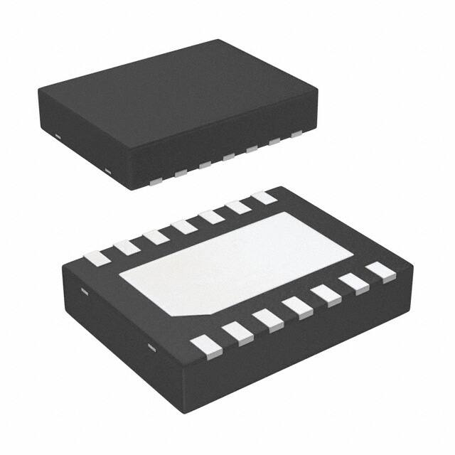
The LM27951 is available in a 14-pin no-pullback
WSON package.
Device Information(1)
PART NUMBER
PACKAGE
LM27951
WSON (14)
BODY SIZE (NOM)
4.00 mm × 3.00 mm
(1) For all available packages, see the orderable addendum at
the end of the data sheet.
Simplified Schematic
VIN = 3 V to 5.5 V
VOUT
VIN
C 1+
CIN
COUT
C1
IDX = 30 mA max
C 1C 2+
D4
LM27951
D4
D3
C2
D3
D2
C 2-
D2
D1
D1
ISET
PWM
GND
EN
RSET
1
An IMPORTANT NOTICE at the end of this data sheet addresses availability, warranty, changes, use in safety-critical applications,
intellectual property matters and other important disclaimers. PRODUCTION DATA.
�LM27951
SNVS416C – NOVEMBER 2005 – REVISED FEBRUARY 2016
www.ti.com
Table of Contents
1
2
3
4
5
6
7
Features ..................................................................
Applications ...........................................................
Description .............................................................
Revision History.....................................................
Pin Configuration and Functions .........................
Specifications.........................................................
1
1
1
2
3
4
6.1
6.2
6.3
6.4
6.5
6.6
4
4
4
4
5
6
Absolute Maximum Ratings ......................................
ESD Ratings..............................................................
Recommended Operating Conditions.......................
Thermal Information ..................................................
Electrical Characteristics...........................................
Typical Characteristics ..............................................
Detailed Description .............................................. 7
7.1 Overview ................................................................... 7
7.2 Functional Block Diagram ......................................... 7
7.3 Feature Description................................................... 7
7.4 Device Functional Modes.......................................... 8
8
Application and Implementation .......................... 9
8.1 Application Information.............................................. 9
8.2 Typical Application ................................................. 10
9 Power Supply Recommendations...................... 12
10 Layout................................................................... 13
10.1 Layout Guidelines ................................................. 13
10.2 Layout Example .................................................... 13
11 Device and Documentation Support ................. 14
11.1
11.2
11.3
11.4
11.5
11.6
Device Support......................................................
Documentation Support ........................................
Community Resources..........................................
Trademarks ...........................................................
Electrostatic Discharge Caution ............................
Glossary ................................................................
14
14
14
14
14
14
12 Mechanical, Packaging, and Orderable
Information ........................................................... 14
4 Revision History
NOTE: Page numbers for previous revisions may differ from page numbers in the current version.
Changes from Revision B (May 2013) to Revision C
•
Added Device Information and Pin Configuration and Functions sections, ESD Ratings and Thermal Information
tables, Feature Description, Device Functional Modes, Application and Implementation, Power Supply
Recommendations, Layout, Device and Documentation Support, and Mechanical, Packaging, and Orderable
Information sections................................................................................................................................................................ 1
Changes from Revision A (May 2013) to Revision B
•
2
Page
Page
Changed layout of National Data Sheet to TI format ........................................................................................................... 13
Submit Documentation Feedback
Copyright © 2005–2016, Texas Instruments Incorporated
Product Folder Links: LM27951
�LM27951
www.ti.com
SNVS416C – NOVEMBER 2005 – REVISED FEBRUARY 2016
5 Pin Configuration and Functions
NHK Package
14-Pin WSON
Top View
NHK Package
14-Pin WSON
Bottom View
C2+
1
14
C1-
VOUT
2
13
GND
C1+
3
12
D4
4
D3
C1-
14
1
C2+
GND
13
2
VOUT
C2-
C2-
12
3
C1+
11
VIN
VIN
11
4
D4
5
10
PWM
PWM
10
5
D3
D2
6
9
EN
EN
9
6
D2
D1
7
8
ISET
I SET
8
7
D1
Die-Attach Pad: GND
Die-Attach Pad: GND
Pin Functions
PIN
NUMBER
NAME
TYPE
DESCRIPTION
1
C2+
Power
Flying capacitor C2 connection
2
VOUT
Power
Pre-regulated charge-pump output
3
C1+
Power
Flying capacitor C1 connection
4
D4
Output
Regulated current source output
5
D3
Output
Regulated current source output
6
D2
Output
Regulated current source output
7
D1
Output
Regulated current source output
8
ISET
Input
Current set input. Placing a resistor (RSET) between this pin and GND sets the LED
current for all the LEDs. LED current = 200 × (1.25 V / RSET).
9
EN
Input
Enable logic input pin. Logic low = shutdown; Logic high = enabled. There is a 150-kΩ
(typical) resistor connected internally between the EN pin and GND.
10
PWM
Input
Current source modulation logic input pin. Logic low = Off; Logic high = On.
Applying a pulse width modulated (PWM) signal to this pin allows the regulated current
sources to be modulated without shutting down the internal charge pump and the VOUT
node.
Input supply: 2.8 V to 5.5 V
11
VIN
Input
12
C2-
Power
Flying capacitor C2 connection
13
GND
Ground
Power supply ground connection
14
C1-
Power
Flying capacitor C1 connection
Submit Documentation Feedback
Copyright © 2005–2016, Texas Instruments Incorporated
Product Folder Links: LM27951
3
�LM27951
SNVS416C – NOVEMBER 2005 – REVISED FEBRUARY 2016
www.ti.com
6 Specifications
6.1 Absolute Maximum Ratings
over operating free-air temperature range (unless otherwise noted) (1) (2)
VIN
EN, PWM
MIN
MAX
–0.3
6
–0.3
Continuous power dissipation
VIN + 0.3
Lead temperature (Soldering, 5 sec.)
Storage temperature, Tstg
(2)
(3)
V
(3)
V
Internally limited
Junction temperature, TJ-MAX-ABS
(1)
UNIT
–65
150
°C
260
°C
150
°C
Stresses beyond those listed under Absolute Maximum Ratings may cause permanent damage to the device. These are stress ratings
only, which do not imply functional operation of the device at these or any other conditions beyond those indicated under Recommended
Operating Conditions. Exposure to absolute-maximum-rated conditions for extended periods may affect device reliability.
If Military/Aerospace specified devices are required, contact the Texas Instruments Sales Office / Distributors for availability and
specifications.
Maximum value is 6 V.
6.2 ESD Ratings
V(ESD)
(1)
Electrostatic discharge
Human-body model (HBM), per ANSI/ESDA/JEDEC JS-001
(1)
VALUE
UNIT
±2000
V
JEDEC document JEP155 states that 500-V HBM allows safe manufacturing with a standard ESD control process.
6.3 Recommended Operating Conditions
over operating free-air temperature range (unless otherwise noted) (1) (2) (3)
MIN
NOM
MAX
UNIT
Inpu voltage, VIN
2.8
5.5
LED voltage
2.5
3.9
V
Junction temperature, TJ
–40
115
°C
Ambient temperature, TA
–40
85
°C
(1)
(2)
(3)
V
All voltages are with respect to the potential at the GND pin.
Minimum and maximum limits are ensured by design, test, or statistical analysis. Typical numbers are not ensured, but do represent the
most likely norm.
In applications where high power dissipation and/or poor package thermal resistance is present, the maximum ambient temperature may
have to be derated. Maximum ambient temperature (TA-MAX) is dependent on the maximum operation junction temperature (TJ-MAX-OP =
115°C), the maximum power dissipation of the device in the application (PD-MAX), and the junction-to ambient thermal resistance of the
part/package in the application (RθJA), as given by the equation: TA-MAX = TJ-MAX-OP – (RθJA × PD-MAX).
6.4 Thermal Information
LM27951
THERMAL METRIC
(1)
NHK (WSON)
UNIT
14 PINS
RθJA
Junction-to-ambient thermal resistance
42.5
°C/W
RθJC(top)
Junction-to-case (top) thermal resistance
33.3
°C/W
RθJB
Junction-to-board thermal resistance
14.1
°C/W
ψJT
Junction-to-top characterization parameter
0.5
°C/W
ψJB
Junction-to-board characterization parameter
14.1
°C/W
RθJC(bot)
Junction-to-case (bottom) thermal resistance
6.1
°C/W
(1)
4
For more information about traditional and new thermal metrics, see the Semiconductor and IC Package Thermal Metrics application
report, SPRA953.
Submit Documentation Feedback
Copyright © 2005–2016, Texas Instruments Incorporated
Product Folder Links: LM27951
�LM27951
www.ti.com
SNVS416C – NOVEMBER 2005 – REVISED FEBRUARY 2016
6.5 Electrical Characteristics
Unless otherwise noted, typical limits are for TA = 25°C, and minimum and maximum limits apply over the full operating
temperature (–40°C to +85°C); specifications apply to the Simplified Schematic with VIN = 3.6 V, V(EN) = 1.8 V, V(PWM) =
1.8 V, 4 LEDs, VDX = 3.6 V, CIN = COUT = 3.3 µF, C1 = C2 = 1 µF, RSET = 12.5 kΩ (1) (2).
PARAMETER
TEST CONDITIONS
3 V ≤ VIN ≤ 5.5 V
RSET = 12.5 kΩ
IVOUT = 0 mA
IDX
LED current regulation
MIN
TYP
MAX
18.4
(−8%)
20
21.6
(8%)
3 V ≤ VIN ≤ 5.5 V
RSET = 8.32 kΩ
IVOUT = 0 mA
30
3 V ≤ VIN ≤ 5.5 V
RSET = 24.9 kΩ
IVOUT = 0 mA
10
UNIT
mA
ID-MATCH
LED current matching (3)
RSET = 8.32 kΩ
0.2
1.5%
IQ
Quiescent supply current
D(1-4) = OPEN
RSET = OPEN
1.5
1.9
mA
ISD
Shutdown supply current
3 V ≤ VIN ≤ 5.5 V
V(EN) = 0 V
0.1
1
µA
VSET
ISET pin voltage
3 V ≤ VIN ≤ 5.5 V
1.25
IDX / ISET
Output current to current set
ratio
Current source voltage
headroom requirement (4)
VHR
V
200
IDX = 95% IDX (nominal)
RSET = 8.32 kΩ
(IDX nominal = 30 mA)
360
IDX = 95% IDX (nom.)
RSET = 12.5 kΩ
(IDX nom. = 20 mA)
240
mV
525
(–30%)
Switching frequency
VIH
Logic input high
Input pins: EN, PWM
3 V ≤ VIN ≤ 5.5 V
1
VIN
VIL
Logic input low
Input pins: EN, PWM
3 V ≤ VIN ≤ 5.5 V
0
0.4
IIH
Logic input high current
750
975
(30%)
fSW
kHz
V
Input pin: PWM
V(PWM) = 1.8 V
10
nA
Input pin: EN
V(EN) = 1.8 V (5)
12
µA
Input pins: EN, PWM
V(EN, PWM) = 0 V
10
nA
3.3
Ω
IIL
Logic input low current
ROUT
Charge pump output
resistance (6)
VGDX
1× to 3/2× gain transition
voltage threshold on VDX
(VOUT − VDX) Falling
500
mV
tON
Start-up time
IDX = 90% steady state
330
µs
(1)
(2)
(3)
(4)
(5)
(6)
All voltages are with respect to the potential at the GND pin.
CIN, COUT, C1, C2: Low-ESR surface-mount ceramic capacitors (MLCCs) used in setting electrical characteristics.
LED current matching is based on two calculations: [(IMAX – IAVG) / IAVG] and [(IAVG – IMIN) / IAVG]. IMAX and IMIN are the highest and
lowest respective Dx currents, and IAVG is the average Dx current of all four current sources. The largest number of the two calculations
(worst case) is considered the matching figure for the part. The typical specification provided is the most likely norm of the matching
figure for all parts.
Headroom voltage (VHR) = VOUT − VDX. If headroom voltage requirement is not met, LED current regulation may be compromised.
EN logic input high current (IIH) is due to a 150-kΩ (typical) pulldown resistor connected internally between the EN and GND pins.
The open-loop output resistance (ROUT) models all voltage losses in the charge pump. ROUT can be used to estimate the voltage at the
charge pump output VOUT and the maximum current capability of the device under low VIN and high IOUT conditions, beyond what is
specified in the electrical specifications table: VOUT = (G × VIN) – (ROUT × IOUT). In the equation, G is the charge-pump-gain mode, and
IOUT is the total output current (sum of all active Dx current sources and all current drawn from VOUT).
Submit Documentation Feedback
Copyright © 2005–2016, Texas Instruments Incorporated
Product Folder Links: LM27951
5
�LM27951
SNVS416C – NOVEMBER 2005 – REVISED FEBRUARY 2016
www.ti.com
6.6 Typical Characteristics
Unless otherwise specified: TA = 25°C, 4 LEDs, VDX = 3.6 V, VIN = 3.6 V, VEN = VIN, VPWM = VIN, C1 = C2 = 1µF, CIN = COUT =
3.3 µF. Capacitors are low-ESR multi-layer ceramic capacitors (MLCCs).
Figure 1. LED Current Regulation vs Input Voltage
VIN = 3.6V
Time scale: 400
Load = 15 mA/LED, 4
ns/Div
LEDs
CH1 (TOP): VIN; Scale: 20mV/Div, AC Coupled
CH2 (BOTTOM): VOUT; Scale: 20mV/Div, AC Coupled
Figure 2. Average LED Current Regulation vs Input Voltage
VIN = 3.6 V
Time scale: 100
µs/Div
CH1 (TOP): VEN; Scale: 1 V/Div
CH2 (BOTTOM): VOUT; Scale: 1 V/Div
Figure 3. Input and Output Voltage Ripple
6
Submit Documentation Feedback
Load = 20mA/LED, 4
LEDs
Figure 4. Start-Up Response
Copyright © 2005–2016, Texas Instruments Incorporated
Product Folder Links: LM27951
�LM27951
www.ti.com
SNVS416C – NOVEMBER 2005 – REVISED FEBRUARY 2016
7 Detailed Description
7.1 Overview
The LM27951 is an adaptive 1.5×/1× CMOS charge pump, optimized for driving white LEDs used in small-format
display backlighting. It provides four constant current outputs capable of sourcing up to 30 mA through each
LED. The well-matched current sources ensure the current through all the LEDs are virtually identical, providing
a uniform brightness across the entire display.
Each current source is internally connected to the charge pump output, VOUT. LED drive current is programmed
by connecting a resistor, RSET, to the current set pin, ISET. LED brightness is adjusted by applying a pulse width
modulated (PWM) signal to the dedicated PWM input pin.
7.2 Functional Block Diagram
LM27951
VOUT
VIN
COUT
3.3 µF
CIN
3.3 µF
OSC
C1+
1 µF
C1C2+
1x/1.5x
Charge
Pump
Voltage
Reference
Gain
Select
PWM
1 µF
D1
D1
C2Regulated
Current Sources
D2
D3
EN
ISET
D2
D4
Current
Control
D3
D4
RSET
GND
7.3 Feature Description
7.3.1 Charge Pump
The input to the 1.5×/1× charge pump is connected to the VIN pin, and the loosely regulated output of the charge
pump is connected to the VOUT pin. The recommended input voltage range of the LM27951 is 3 V to 5.5 V. The
loosely regulated charge pump of the device has both open loop and closed loop modes of operation. When the
device is in open loop, the voltage at VOUT is equal to the gain times the voltage at the input. When the device is
in closed loop, the voltage at VOUT is loosely regulated to 4.5 V (typical). The charge pump gain transitions are
actively selected to maintain regulation based on LED forward voltage and load requirements. This allows the
charge pump to stay in the most efficient gain (1×) over as much of the input voltage range as possible, reducing
the power consumed from the battery.
7.3.2 Soft Start
The LM27951 contains internal soft-start circuitry to limit input inrush currents when the part is enabled. Soft start
is implemented internally with a controlled turnon of the internal voltage reference. Due to the soft-start circuitry,
startup time of the LM27951 is approximately 330 µs (typical).
7.3.3 Thermal Protection
Internal thermal protection circuitry disables the LM27951 when the junction temperature exceeds 150°C
(typical). This feature protects the device from being damaged by high die temperatures that might otherwise
result from excessive power dissipation. The device recovers and operate normally when the junction
temperature falls below 140°C (typical). It is important that the board layout provide good thermal conduction to
keep the junction temperature within the specified operating ratings.
Submit Documentation Feedback
Copyright © 2005–2016, Texas Instruments Incorporated
Product Folder Links: LM27951
7
�LM27951
SNVS416C – NOVEMBER 2005 – REVISED FEBRUARY 2016
www.ti.com
7.4 Device Functional Modes
7.4.1 Enable and PWM Pins
The LM27951 has 2 logic control pins. Both pins are active-high logic (HIGH = ON). There is an internal pulldown
resistor (150 kΩ typical) connected between the enable pin (EN) and GND. There is no pullup or pulldown
connected to the pulse width modulated (PWM) pin.
The EN pin is the master enable pin for the part. When the voltage on this pin is low (< 0.4 V), the part is in
shutdown mode. In this mode, all internal circuitry is OFF and the part consumes very little supply current (< 1 µA
typical). When the voltage on the EN pin is high (> 1 V), the device activates the charge pump and regulate the
output voltage to its nominal value.
The PWM pin serves as a dedicated logic input for LED brightness control. When the voltage on this pin is low (<
0.4 V), the current sources are turned off, and no current flows through the LEDs. When the voltage on this pin is
high (> 1 V), the currents sources turn on and regulate to the current level set by the resistor connected to the
ISET pin.
7.4.2 Adjusting LED Brightness (PWM Control)
Perceived LED brightness can be adjusted using a PWM control signal on the LM27951 PWM logic input pin,
turning the current sources ON and OFF at a rate faster than perceptible by the human eye. When this is done,
the total brightness perceived is proportional to the duty cycle (D) of the PWM signal (D = the percentage of time
that the LED is on in every PWM cycle). A simple example: if the LEDs are driven at 15 mA each with a PWM
signal that has a 50% duty cycle, perceived LED brightness is about half as bright as compared to when the
LEDs are driven continuously with 15 mA.
The minimum recommended PWM frequency is 100 Hz. Frequencies below this may be visible as flicker or
blinking. The maximum recommended PWM frequency is 1 kHz. Frequencies above this may cause interference
with internal current driver circuitry and/or noise in the audible range. Due to the regulation control loop, the
maximum frequency and minimum duty cycle applied to the PWM pin must be chosen such that the minimum
ON time is no less than 30 µs in duration. If a PWM signal is applied to the EN pin instead, the maximum
frequency and minimum duty cycle should be chosen to accommodate both the LM27951 start-up time (330 µs
typical) and the 30-µs control loop delay.
The preferred method to adjust brightness is to keep the master EN voltage ON continuously and apply a PWM
signal to the dedicated PWM input pin. The benefit of this type of connection can be best understood with a
contrary example. When a PWM signal is connected to the master enable (EN) pin, the charge pump repeatedly
turns on and off. Every time the charge pump turns on, there is an inrush of current as the capacitors, both
internal and external, are recharged. This inrush current results in a current spike and a voltage dip at the input
of the part. By applying the PWM signal to PWM logic input pin, the charge pump remains active, resulting in
much lower input noise.
When the PWM signal must be connected to the EN pin, measures can be taken to reduce the magnitude of the
charge-pump turnon transient response. More input capacitance, series resistors, and/or ferrite beads may
provide benefits. If the current spikes and voltage dips can be tolerated, connecting the PWM signal to the EN
pin does provide a benefit of lower supply current consumption. When the PWM signal to the EN pin is low, the
LM27951 is shut down, and the input current is only a few micro-amps. This results in a lower time-averaged
input current than the prior suggestion, where EN is kept on continuously.
8
Submit Documentation Feedback
Copyright © 2005–2016, Texas Instruments Incorporated
Product Folder Links: LM27951
�LM27951
www.ti.com
SNVS416C – NOVEMBER 2005 – REVISED FEBRUARY 2016
8 Application and Implementation
NOTE
Information in the following applications sections is not part of the TI component
specification, and TI does not warrant its accuracy or completeness. TI’s customers are
responsible for determining suitability of components for their purposes. Customers should
validate and test their design implementation to confirm system functionality.
8.1 Application Information
8.1.1 Maximum Output Current, Maximum LED Voltage, Minimum Input Voltage
The LM27951 can drive 4 LEDs at 30 mA each from an input voltage as low as 3 V, so long as the LEDs have a
forward voltage of 3.6 V or less (room temperature).
The previous statement is a simple example of the LED drive capabilities of the LM27951. The statement
contains key application parameters required to validate an LED-drive design using the LM27951: LED current
(ILED), number of active LEDs (N), LED forward voltage (VLED), and minimum input voltage (VIN-MIN).
Equation 1 can be used to estimate the total output current capability of the LM27951:
ILED_MAX = ((1.5 × VIN) – VLED) / ((N × ROUT) + kHR
where
•
ROUT = output resistance
(1)
As an example of Equation 1: ILED_MAX = ((1.5 × VIN ) – VLED) / ((N × 3.3 Ω) + 12 mV/mA).
This parameter models the internal losses of the charge pump that result in voltage droop at the pump output
VOUT. Because the magnitude of the voltage droop is proportional to the total output current of the charge pump,
the loss parameter is modeled as a resistance. The output resistance of the LM27951 is typically 3.3 Ω (VIN = 3
V, TA = 25°C – see Equation 2).
VVOUT = 1.5 × VIN – N × ILED × ROUT
where
•
•
kHR = headroom constant
ROUT = output resistance
(2)
This parameter models the minimum voltage required across the current sources for proper regulation. This
minimum voltage is proportional to the programmed LED current, so the constant has units of mV/mA. The
typical kHR of the LM27951 is 12 mV/mA – see Equation 3:
(VVOUT – VLED) > kHR × ILED
(3)
Maximum LED current is highly dependent on minimum input voltage and LED forward voltage. Output current
capability can be increased by raising the minimum input voltage of the application, or by selecting LEDs with a
lower forward voltage. Excessive power dissipation may also limit output current capability of an application.
Submit Documentation Feedback
Copyright © 2005–2016, Texas Instruments Incorporated
Product Folder Links: LM27951
9
�LM27951
SNVS416C – NOVEMBER 2005 – REVISED FEBRUARY 2016
www.ti.com
8.2 Typical Application
VIN = 3 V to 5.5 V
VOUT
VIN
C 1+
3.3 µF
CIN
C1
3.3 µF
COUT
1 µF
IDX = 30 mA max
C 1C 2+
D4
LM27951
C2
D4
D3
1 µF
D3
D2
C 2-
D2
D1
D1
ISET
PWM
GND
EN
RSET
Capacitors: 1 µF - TDK C1608X7R1C105K
3.3 µF - TDK C1608X5R1A335K
Figure 5. LM27951 Typical Application
8.2.1 Design Requirements
For typical white-LED switched capacitor applications, use the parameters listed in Table 1.
Table 1. Design Parameters
DESIGN PARAMETER
EXAMPLE VALUE
Minimum input voltage
2.8 V
Output current
20 mA
RSET
12.5 kΩ
8.2.2 Detailed Design Procedure
8.2.2.1 Setting LED Currents
The current through the four LEDs connected to D1-4 can be set to a desired level simply by connecting an
appropriately sized resistor (RSET) between the ISET pin of the LM27951 and GND. The LED currents are
proportional to the current that flows out of the ISET pin and are a factor of 200 times greater than the ISET current.
The feedback loop of an internal amplifier sets the voltage of the ISET pin to 1.25 V (typical). The previous
statements are simplified in Equation 4 and Equation 5:
IDx = 200 × (VSET / RSET)
RSET = 200 × (1.25 V / IDx)
(4)
(5)
8.2.2.2 Capacitor Selection
The LM27951 requires 4 external capacitors for proper operation. Surface-mount multi-layer ceramic capacitors
are recommended. These capacitors are small, inexpensive and have very low equivalent series resistance
(ESR) — < 20 mΩ typical. Tantalum capacitors, OS-CON capacitors, and aluminum electrolytic capacitors are
not recommended for use with the LM27951 due to their high ESR, compared to ceramic capacitors.
For most applications, it is preferable to use ceramic capacitors with X7R or X5R temperature characteristic with
the LM27951. These capacitors have tight capacitance tolerance (as good as ±10%) and hold their value over
temperature (X7R: ±15% over –55°C to 125°C; X5R: ±15% over –55°C to +85°C).
10
Submit Documentation Feedback
Copyright © 2005–2016, Texas Instruments Incorporated
Product Folder Links: LM27951
�LM27951
www.ti.com
SNVS416C – NOVEMBER 2005 – REVISED FEBRUARY 2016
Capacitors with Y5V or Z5U temperature characteristic are generally not recommended for use with the
LM27951. Capacitors with these temperature characteristics typically have wide capacitance tolerance (80%,
–20%) and vary significantly over temperature (Y5V: 22%, –82% over –30°C to +85°C range; Z5U: 22%, –56%
over 10°C to 85°C range). Under some conditions, a nominal 1-µF Y5V or Z5U capacitor could have a
capacitance of only 0.1 µF. Such detrimental deviation is likely to cause Y5V and Z5U capacitors to fail to meet
the minimum capacitance requirements of the LM27951.
The voltage rating of the output capacitor must be 10 V or more. All other capacitors must have a voltage rating
at or above the maximum input voltage of the application.
8.2.2.3 Parallel Dx Outputs for Increased Current Drive
Outputs D1-4 may be connected together to drive a one or two LEDs at higher currents. In a one LED
configuration, all four parallel current sources of equal value are connected together to drive a single LED. The
LED current programmed must be chosen such that the current provided from each of the outputs is
programmed to 25% of the total desired LED current. For example, if 60 mA is the desired drive current for the
single LED, RSET must be selected so that the current out of each current source is 15 mA. Similarly, if two LEDs
are to be driven by pairing up the D1-4 outputs (that is, D1-2, D3-4), RSET must be selected so that the current out of
each current source output is 50% of the desired LED current.
Connecting the outputs in parallel does not affect the internal operation of the LM27951 and has no impact on
the electrical characteristics and limits previously presented. The available diode output current, maximum diode
voltage, and all other specifications provided in the Electrical Characteristics apply to this parallel output
configuration, just as they do to the standard 4-LED application circuit.
8.2.2.4 Power Efficiency
Efficiency of LED drivers is commonly taken to be the ratio of power consumed by the LEDs (PLED) to the power
drawn at the input of the part (PIN). With a 1.5×/1× charge pump, the input current is equal to the charge pump
gain times the output current (total LED current). For a simple approximation, the current consumed by internal
circuitry can be neglected and the efficiency of the LM27951 can be predicted as follows:
PLED = N × VLED × ILED
PIN = VIN × IIN
PIN = VIN × (Gain × N × ILED + IQ)
E = (PLED / PIN)
(6)
(7)
(8)
(9)
Neglecting IQ results in a slightly higher efficiency prediction, but this impact is no more than a few percentage
points when several LEDs are driven at full power. It is also worth noting that efficiency as defined here is in part
dependent on LED voltage. Variation in LED voltage does not affect power consumed by the circuit and typically
does not relate to the brightness of the LED. For an advanced analysis, it is recommended that power consumed
by the circuit (VIN × IIN) be evaluated rather than power efficiency.
8.2.2.5 Power Dissipation
The power dissipation (PDISSIPATION) and junction temperature (TJ) can be approximated with Equation 10 and
Equation 11. PIN is the power generated by the 1.5×/1× charge pump, PLED is the power consumed by the LEDs,
TAis the ambient temperature, and RθJA is the junction-to-ambient thermal resistance for the 14-pin WSON
package. VIN is the input voltage to the LM27951, VLED is the nominal LED forward voltage, and ILED is the
programmed LED current.
PDISSIPATION = PIN – PLED = [Gain × VIN × (4 x ILED)] − (VLED × 4 × ILED)
TJ = TA + (PDISSIPATION × RθJA)
(10)
(11)
The junction temperature rating takes precedence over the ambient temperature rating. The LM27951 may be
operated outside the ambient temperature rating, so long as the junction temperature of the device does not
exceed the maximum operating rating of 115°C. The maximum ambient temperature rating must be derated in
applications where high power dissipation and/or poor thermal resistance causes the junction temperature to
exceed 115°C.
Submit Documentation Feedback
Copyright © 2005–2016, Texas Instruments Incorporated
Product Folder Links: LM27951
11
�LM27951
SNVS416C – NOVEMBER 2005 – REVISED FEBRUARY 2016
www.ti.com
8.2.3 Application Curves
Figure 6. Converter Efficiency vs Input Voltage
Figure 7. LED Current vs RSET
9 Power Supply Recommendations
The LM27951 is designed to operate from an input voltage supply range from 2.8 V to 5.5 V. This input supply
must be well regulated and capable to supply the required input current. If the input supply is located far from the
device, additional bulk capacitance may be required in addition to the ceramic bypass capacitors.
12
Submit Documentation Feedback
Copyright © 2005–2016, Texas Instruments Incorporated
Product Folder Links: LM27951
�LM27951
www.ti.com
SNVS416C – NOVEMBER 2005 – REVISED FEBRUARY 2016
10 Layout
10.1 Layout Guidelines
The WSON is a leadframe-based chip scale package (CSP) with very good thermal properties. This package has
an exposed DAP (die attach pad) thermal pad at the center of the package measuring 3 mm × 1.6 mm. The main
advantage of this exposed DAP is to offer lower thermal resistance when it is soldered to the thermal land on the
PCB. For PCB layout, TI highly recommends a 1:1 ratio between the package and the PCB thermal land. To
further enhance thermal conductivity, the PCB thermal land may include vias to a ground plane. For more
detailed instructions on mounting WSON packages, refer to AN-1187 Leadless Leadframe Package (LLP)
SNOA401.
10.2 Layout Example
LM27951
C1-
C2+
GND
C1+
D4
D3
THERMAL PAD
VOUT
C2VIN
PWM
D2
EN
D1
ISET
CONNECT TO GND
PLANE
Figure 8. LM27951 Layout Example
Submit Documentation Feedback
Copyright © 2005–2016, Texas Instruments Incorporated
Product Folder Links: LM27951
13
�LM27951
SNVS416C – NOVEMBER 2005 – REVISED FEBRUARY 2016
www.ti.com
11 Device and Documentation Support
11.1 Device Support
11.1.1 Third-Party Products Disclaimer
TI'S PUBLICATION OF INFORMATION REGARDING THIRD-PARTY PRODUCTS OR SERVICES DOES NOT
CONSTITUTE AN ENDORSEMENT REGARDING THE SUITABILITY OF SUCH PRODUCTS OR SERVICES
OR A WARRANTY, REPRESENTATION OR ENDORSEMENT OF SUCH PRODUCTS OR SERVICES, EITHER
ALONE OR IN COMBINATION WITH ANY TI PRODUCT OR SERVICE.
11.2 Documentation Support
11.2.1 Related Documentation
For additional information, see the following:
AN-1187 Leadless Leadframe Package (LLP) (SNOA401)
11.3 Community Resources
The following links connect to TI community resources. Linked contents are provided "AS IS" by the respective
contributors. They do not constitute TI specifications and do not necessarily reflect TI's views; see TI's Terms of
Use.
TI E2E™ Online Community TI's Engineer-to-Engineer (E2E) Community. Created to foster collaboration
among engineers. At e2e.ti.com, you can ask questions, share knowledge, explore ideas and help
solve problems with fellow engineers.
Design Support TI's Design Support Quickly find helpful E2E forums along with design support tools and
contact information for technical support.
11.4 Trademarks
E2E is a trademark of Texas Instruments.
All other trademarks are the property of their respective owners.
11.5 Electrostatic Discharge Caution
These devices have limited built-in ESD protection. The leads should be shorted together or the device placed in conductive foam
during storage or handling to prevent electrostatic damage to the MOS gates.
11.6 Glossary
SLYZ022 — TI Glossary.
This glossary lists and explains terms, acronyms, and definitions.
12 Mechanical, Packaging, and Orderable Information
The following pages include mechanical, packaging, and orderable information. This information is the most
current data available for the designated devices. This data is subject to change without notice and revision of
this document. For browser-based versions of this data sheet, refer to the left-hand navigation.
14
Submit Documentation Feedback
Copyright © 2005–2016, Texas Instruments Incorporated
Product Folder Links: LM27951
�PACKAGE OPTION ADDENDUM
www.ti.com
10-Dec-2020
PACKAGING INFORMATION
Orderable Device
Status
(1)
Package Type Package Pins Package
Drawing
Qty
Eco Plan
(2)
Lead finish/
Ball material
MSL Peak Temp
Op Temp (°C)
Device Marking
(3)
(4/5)
(6)
LM27951SD/NOPB
ACTIVE
WSON
NHK
14
1000
RoHS & Green
SN
Level-1-260C-UNLIM
-40 to 85
D006B
LM27951SDX/NOPB
ACTIVE
WSON
NHK
14
4500
RoHS & Green
SN
Level-1-260C-UNLIM
-40 to 85
D006B
(1)
The marketing status values are defined as follows:
ACTIVE: Product device recommended for new designs.
LIFEBUY: TI has announced that the device will be discontinued, and a lifetime-buy period is in effect.
NRND: Not recommended for new designs. Device is in production to support existing customers, but TI does not recommend using this part in a new design.
PREVIEW: Device has been announced but is not in production. Samples may or may not be available.
OBSOLETE: TI has discontinued the production of the device.
(2)
RoHS: TI defines "RoHS" to mean semiconductor products that are compliant with the current EU RoHS requirements for all 10 RoHS substances, including the requirement that RoHS substance
do not exceed 0.1% by weight in homogeneous materials. Where designed to be soldered at high temperatures, "RoHS" products are suitable for use in specified lead-free processes. TI may
reference these types of products as "Pb-Free".
RoHS Exempt: TI defines "RoHS Exempt" to mean products that contain lead but are compliant with EU RoHS pursuant to a specific EU RoHS exemption.
Green: TI defines "Green" to mean the content of Chlorine (Cl) and Bromine (Br) based flame retardants meet JS709B low halogen requirements of


 工商网监
湘ICP备2023018690号
工商网监
湘ICP备2023018690号
