LM2852
www.ti.com
SNVS325D – JANUARY 2005 – REVISED APRIL 2013
LM2852 2A 500/1500kHz Synchronous SIMPLE SWITCHER® Buck Regulator
Check for Samples: LM2852
FEATURES
DESCRIPTION
•
•
The LM2852 SIMPLE SWITCHER® synchronous
buck regulator is a high frequency step-down
switching voltage regulator capable of driving up to a
2A load with excellent line and load regulation. The
LM2852 can accept an input voltage between 2.85V
and 5.5V and deliver an output voltage that is factory
programmable from 0.8V to 3.3V in 100mV
increments. The LM2852 is available with a choice of
two switching frequencies - 500kHz (LM2852Y) or
1.5MHz (LM2852X). It also features internal, typethree compensation to deliver a low component count
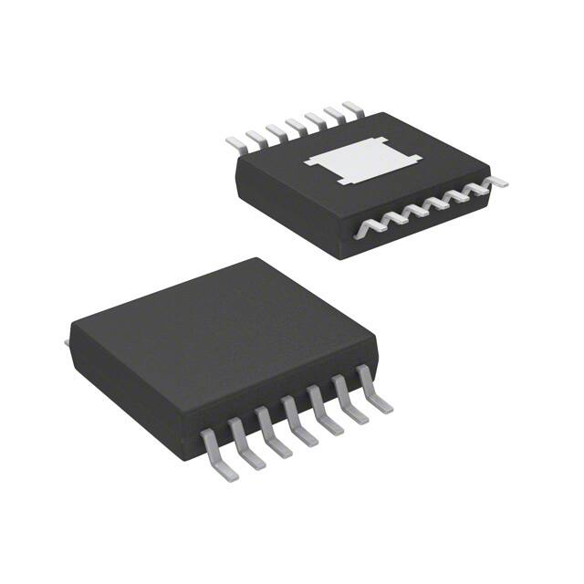
solution. The exposed-pad HTSSOP-14 package
enhances the thermal performance of the LM2852.
1
2
•
•
•
•
•
•
•
Input Voltage Range of 2.85 to 5.5V
Factory EEPROM Set Output Voltages from
0.8V to 3.3V in 100mV Increments
Maximum Load Current of 2A
Voltage Mode Control
Internal Type-Three Compensation
Switching Frequency of 500kHz or 1.5MHz
Low Standby Current of 10µA
Internal 60 mΩ MOSFET Switches
Standard Voltage Options
0.8/1.0/1.2/1.5/1.8/2.5/3.3 Volts
APPLICATIONS
•
•
•
•
Low Voltage Point of Load Regulation
Local Solution for FPGA/DSP/ASIC Core
Power
Broadband Networking and Communications
Infrastructure
Portable Computing
Typical Application Circuit
VIN = 3.3V
PVIN
CIN = 22 PF
AVIN
EN
SS
LM2852Y
SNS
VOUT = 2.5V
ILOAD = 0A to 2A
SW
SGND
PGND
LO = 10 PH
+
CO = 100 PF
CSS = 2.7 nF
1
2
Please be aware that an important notice concerning availability, standard warranty, and use in critical applications of
Texas Instruments semiconductor products and disclaimers thereto appears at the end of this data sheet.
All trademarks are the property of their respective owners.
PRODUCTION DATA information is current as of publication date.
Products conform to specifications per the terms of the Texas
Instruments standard warranty. Production processing does not
necessarily include testing of all parameters.
Copyright © 2005–2013, Texas Instruments Incorporated
�LM2852
SNVS325D – JANUARY 2005 – REVISED APRIL 2013
www.ti.com
Figure 1. Efficiency vs ILOAD
96
PVIN = 3.3V
EFFICIENCY (%)
94
92
90
88
86
84
0.1
1.0
10
ILOAD (A)
Connection Diagram
AVIN
1
14
SNS
EN
2
13
NC
SGND
3
12
NC
11
PGND
LM2852
SS
4
NC
5
10
PGND
PVIN
6
9
SW
PVIN
7
8
SW
Figure 2. 14-Pin HTSSOP – Top View
See Package Number PWP0014A
PIN DESCRIPTIONS
AVIN (Pin 1): Chip bias input pin. This provides power to the logic of the chip. Connect to the input voltage or a separate rail.
EN (Pin 2): Enable. Connect this pin to ground to disable the chip; connect to AVIN or leave floating to enable the chip; enable is internally
pulled up.
SGND (Pin 3): Signal ground.
SS (Pin 4): Soft-start pin. Connect this pin to a small capacitor to control startup. The soft-start capacitance range is restricted to values 1
nF to 50 nF.
NC (Pins 5, 12 and 13): No connect. These pins must be tied to ground or left floating in the application.
PVIN (Pins 6, 7): Input supply pin. PVIN is connected to the input voltage. This rail connects to the source of the internal power PFET.
SW (Pins 8, 9): Switch pin. Connect to the output inductor.
PGND (Pins 10, 11): Power ground. Connect this to an internal ground plane or other large ground plane.
SNS (Pin 14): Output voltage sense pin. Connect this pin to the output voltage as close to the load as possible.
Exposed Pad: Connect to ground.
2
Submit Documentation Feedback
Copyright © 2005–2013, Texas Instruments Incorporated
Product Folder Links: LM2852
�LM2852
www.ti.com
SNVS325D – JANUARY 2005 – REVISED APRIL 2013
These devices have limited built-in ESD protection. The leads should be shorted together or the device placed in conductive foam
during storage or handling to prevent electrostatic damage to the MOS gates.
Absolute Maximum Ratings (1) (2)
−0.3V to 6.5V
PVIN, AVIN, EN, SNS
ESD Susceptibility (3)
2kV
Power Dissipation
Internally Limited
Storage Temperature Range
−65°C to +150°C
Maximum Junction Temp.
14-Pin Exposed Pad HTSSOP Package
150°C
Infrared (15 sec)
220°C
Vapor Phase (60 sec)
215°C
Soldering (10 sec)
(1)
(2)
(3)
260°C
Absolute maximum ratings indicate limits beyond which damage to the device may occur. Operating Range indicates conditions for
which the device is intended to be functional, but does not ensure specfic performance limits. For ensured specifications and test
conditions, see the Electrical Characteristics.
If Military/Aerospace specified devices are required, please contact the Texas Instruments Sales Office/ Distributors for availability and
specifications.
Human body model: 1.5kΩ in series with 100pF. SW and PVIN pins are derated to 1.5kV
Operating Ratings (1)
PVIN to GND
1.5V to 5.5V
AVIN to GND
2.85V to 5.5V
−40°C to +125°C
Junction Temperature
θJA
(1)
38°C/W
Absolute maximum ratings indicate limits beyond which damage to the device may occur. Operating Range indicates conditions for
which the device is intended to be functional, but does not ensure specfic performance limits. For ensured specifications and test
conditions, see the Electrical Characteristics.
Submit Documentation Feedback
Copyright © 2005–2013, Texas Instruments Incorporated
Product Folder Links: LM2852
3
�LM2852
SNVS325D – JANUARY 2005 – REVISED APRIL 2013
www.ti.com
Electrical Characteristics
AVIN = PVIN = 5V unless otherwise indicated under the Conditions column. Limits in standard type are for TJ = 25°C only;
limits in boldface type apply over the junction temperature (TJ) range of -40°C to +125°C. Minimum and Maximum limits are
ensured through test, design, or statistical correlation. Typical values represent the most likely parametric norm at TJ = 25°C,
and are provided for reference purposes only.
Symbol
Parameter
Conditions
Min
Typ
Max
Units
SYSTEM PARAMETERS
VOUT
Voltage
Tolerance (1)
ΔVOUT/ΔAVIN
Line Regulation (1)
VOUT = 0.8V option
0.782
0.818
VOUT = 1.0V option
0.9775
1.0225
VOUT = 1.2V option
1.1730
1.2270
VOUT = 1.5V option
1.4663
1.5337
VOUT = 1.8V option
1.7595
1.8405
VOUT = 2.5V option
2.4437
2.5563
VOUT = 3.0V option
2.9325
3.0675
VOUT = 3.3V option
3.2257
3.3743
V
VOUT = 0.8V, 1.0V, 1.2V, 1.5V, 1.8V or 2.5V
2.85V ≤ AVIN ≤ 5.5V
0.2
0.6
%
VOUT = 3.3V
3.5V ≤ AVIN ≤ 5.5V
0.2
0.6
%
ΔVOUT/ΔIO
Load Regulation
Normal operation
VON
UVLO Threshold
(AVIN)
Rising
Falling Hysteresis
8
85
mV/A
2.47
2.85
V
150
210
mV
rDSON-P
PFET On
Resistance
Isw = 2A
75
140
mΩ
rDSON-N
NFET On
Resistance
Isw = 2A
55
120
mΩ
RSS
Soft-start resistance
ICL
Peak Current Limit
Threshold
LM2852X
2.75
4
4.95
LM2852Y
2.25
3
3.65
Operating Current
Non-switching
0.85
2
mA
Shutdown Quiescent
EN = 0V
Current
10
25
µA
RSNS
Sense pin resistance
400
fosc
LM2852X
1500kHz option.
1050
1500
1825
kHz
LM2852Y
500kHz option.
325
500
625
kHz
100
%
IQ
ISD
400
kΩ
A
kΩ
PWM
Drange
Duty Cycle Range
0
ENABLE CONTROL (2)
VIH
EN Pin Minimum
High Input
VIL
EN Pin Maximum
Low Input
IEN
EN Pin Pullup
Current
% of
AVIN
75
25
EN = 0V
% of
AVIN
1.2
µA
THERMAL CONTROLS
(1)
(2)
4
TSD
TJ for Thermal
Shutdown
165
°C
TSD-HYS
Hysteresis for
Thermal Shutdown
10
°C
VOUT measured in a non-switching, closed-loop configuration at the SNS pin.
The enable pin is internally pulled up, so the LM2852 is automatically enabled unless an external enable voltage is applied.
Submit Documentation Feedback
Copyright © 2005–2013, Texas Instruments Incorporated
Product Folder Links: LM2852
�LM2852
www.ti.com
SNVS325D – JANUARY 2005 – REVISED APRIL 2013
LM2852Y Typical Performance Characteristics (500kHz)
Efficiency vs ILoad VOUT = 1.5V
Efficiency vs ILoad VOUT = 2.5V
92
96
PVIN = 3.3V
PVIN = 3.3V
90
94
86
84
92
EFFICIENCY (%)
EFFICIENCY (%)
88
PVIN = 5.0V
82
90
PVIN = 5.0V
88
80
86
78
84
76
0.1
1.0
0.1
10
1.0
10
ILOAD (A)
ILOAD (A)
Figure 3.
Figure 4.
Efficiency vs ILoad VOUT = 3.3V
Frequency vs Temperature
95
560
94
550
VIN = 3.3V
PVIN = 5.0V
540
FREQUENCY (kHz)
EFFICIENCY (%)
93
92
91
90
530
520
510
89
500
88
490
87
0.1
1.0
10
480
-50
VIN = 5V
-25
0
25
50
75
100 125 150
TEMPERATURE (oC)
ILOAD (A)
Figure 5.
Figure 6.
Submit Documentation Feedback
Copyright © 2005–2013, Texas Instruments Incorporated
Product Folder Links: LM2852
5
�LM2852
SNVS325D – JANUARY 2005 – REVISED APRIL 2013
www.ti.com
LM2852X Typical Performance Characteristics (1500kHz)
Efficiency vs ILoad VOUT = 1.5V
Efficiency vs ILoad VOUT = 2.5V
100
85
PVIN = 3.3V
PVIN = 3.3V
80
90
70
65
60
80
EFFICIENCY (%)
EFFICIENCY (%)
75
PVIN = 5.0V
PVIN = 5.0V
70
60
55
50
50
45
0.1
1.0
40
0.1
10
ILOAD (A)
Figure 7.
Figure 8.
Efficiency vs ILoad VOUT = 3.3V
Frequency vs Temperature
1600
85
1550
FREQUENCY (kHz)
EFFICIENCY (%)
80
PVIN = 5.0V
70
65
60
1500
1450
PVIN = 5.0V
1400
1350
1300
1.0
10
1200
-50 -25
0
25
50
75
80
85
90
o
TEMPERATURE ( C)
ILOAD (A)
Figure 9.
6
PVIN = 3.3V
1250
55
50
0.1
10
ILOAD (A)
90
75
1.0
Figure 10.
Submit Documentation Feedback
Copyright © 2005–2013, Texas Instruments Incorporated
Product Folder Links: LM2852
�LM2852
www.ti.com
SNVS325D – JANUARY 2005 – REVISED APRIL 2013
LM2852 Typical Performance Characteristics (Both Y and X Versions)
Shutdown Current vs VIN
Quiescent Current (Non-Switching) vs VIN
1100
17
1000
15
125oC
900
13
o
85 C
IQ (PA)
IQ SHUTDOWN (PA)
125oC
11
o
800
85oC
25 C
25oC
700
9
-40oC
7
5
2.5
3
3.5
4
4.5
5
-40oC
600
500
2.5
5.5
3
3.5
4
4.5
5
5.5
VIN (V)
VIN (V)
Figure 11.
Figure 12.
NMOS Switch RDSON vs Temperature
PMOS Switch RDSON vs Temperature
100
130
120
90
PFET RDSON (m:)
NFET RDSON (m:)
110
80
PVIN = 3.3V
70
PVIN = 5.0V
60
PVIN = 3.3V
100
90
PVIN = 5.0V
80
70
50
60
40
-50
-25
0
25
50
75
100 125 150
TEMPERATURE (oC)
50
-50
-25
0
25
50
75
100 125 150
TEMPERATURE (oC)
Figure 13.
Figure 14.
Submit Documentation Feedback
Copyright © 2005–2013, Texas Instruments Incorporated
Product Folder Links: LM2852
7
�LM2852
SNVS325D – JANUARY 2005 – REVISED APRIL 2013
www.ti.com
Block Diagram
SGND
PVIN
Reference
Oscillator
UVLO
DAC
AVIN
Current Limit
Ramp and Clock
Generator
400 k:
EN
Gate
Drive
Error
Amp
SS
+
20 pF
200 k:
200 k:
Zc1
Zc2
SW
+
PWM
Comp
PGND
SNS
8
Submit Documentation Feedback
Copyright © 2005–2013, Texas Instruments Incorporated
Product Folder Links: LM2852
�LM2852
www.ti.com
SNVS325D – JANUARY 2005 – REVISED APRIL 2013
APPLICATIONS INFORMATION
The LM2852 is a DC-DC synchronous buck regulator belonging to Texas Instrument’s SIMPLE SWITCHER
family. Integration of the PWM controller, power switches and compensation network greatly reduces the
component count required to implement a switching power supply. A typical application requires only four
components: an input capacitor, a soft-start capacitor, an output filter capacitor and an output filter inductor.
INPUT CAPACITOR (CIN)
Fast switching of large currents in the buck converter places a heavy demand on the voltage source supplying
PVIN. The input capacitor, CIN, supplies extra charge when the switcher needs to draw a burst of current from
the supply. The RMS current rating and the voltage rating of the CIN capacitor are therefore important in the
selection of CIN. The RMS current specification can be approximated by:
IRMS = ILOAD
D(1-D)
where
•
D is the duty cycle, VOUT/VIN. CIN also provides filtering of the supply.
(1)
Trace resistance and inductance degrade the benefits of the input capacitor, so CIN should be placed very close
to PVIN in the layout. A 22 µF or 47 µF ceramic capacitor is typically sufficient for CIN. In parallel with the large
input capacitance a smaller capacitor may be added such as a 1µF ceramic for higher frequency filtering.
SOFT-START CAPACITOR (CSS)
The DAC that sets the reference voltage of the error amp sources a current through a resistor to set the
reference voltage. The reference voltage is one half of the output voltage of the switcher due to the 200kΩ
divider connected to the SNS pin. Upon start-up, the output voltage of the switcher tracks the reference voltage
with a two to one ratio as the DAC current charges the capacitance connected to the reference voltage node.
Internal capacitance of 20pF is permanently attached to the reference voltage node which is also connected to
the soft-start pin, SS. Adding a soft-start capacitor externally increases the time it takes for the output voltage to
reach its final level.
The charging time required for the reference voltage can be estimated using the RC time constant of the DAC
resistor and the capacitance connected to the SS pin. Three RC time constant periods are needed for the
reference voltage to reach 95% of its final value. The actual start-up time will vary with differences in the DAC
resistance and higher-order effects.
If little or no soft-start capacitance is connected, then the start-up time may be determined by the time required
for the current limit current to charge the output filter capacitance. The capacitor charging equation I = C ΔV/Δt
can be used to estimate the start-up time in this case. For example, a part with a 3V output, a 100 µF output
capacitance and a 3A current limit threshold would require a time of 100 µs:
't = C
'V
3V
= 100 PF
= 100 Ps
I
3A
(2)
Since it is undesirable for the power supply to start up in current limit, a soft-start capacitor must be chosen to
force the LM2852 to start up in a more controlled fashion based on the charging of the soft-start capacitance. In
this example, suppose a 3 ms start time is desired. Three time constants are required for charging the soft-start
capacitor to 95% of the final reference voltage. So in this case RC=1ms. The DAC resistor, R, is 400 kΩ so C
can be calculated to be 2.5nF. A 2.7nF ceramic capacitor can be chosen to yield approximately a 3ms start-up
time.
SOFT-START CAPACITOR (CSS) AND FAULT CONDITIONS
Various fault conditions such as short circuit and UVLO of the LM2852 activate internal circuitry designed to
control the voltage on the soft-start capacitor. For example, during a short circuit current limit event, the output
voltage typically falls to a low voltage. During this time, the soft-start voltage is forced to track the output so that
once the short is removed, the LM2852 can restart gracefully from whatever voltage the output reached during
the short circuit event. The range of soft-start capacitors is therefore restricted to values 1nF to 50nF.
Submit Documentation Feedback
Copyright © 2005–2013, Texas Instruments Incorporated
Product Folder Links: LM2852
9
�LM2852
SNVS325D – JANUARY 2005 – REVISED APRIL 2013
www.ti.com
COMPENSATION
The LM2852 provides a highly integrated solution to power supply design. The compensation of the LM2852,
which is type-three, is included on-chip. The benefit to integrated compensation is straightforward, simple power
supply design. Since the output filter capacitor and inductor values impact the compensation of the control loop,
the range of L, C and CESR values is restricted in order to ensure stability.
OUTPUT FILTER VALUES
Table 1 details the recommended inductor and capacitor ranges for the LM2852 that are suggested for various
typical output voltages. Values slightly different than those recommended may be used, however the phase
margin of the power supply may be degraded.
Table 1. Output Filter Values
Frequency Option
LM2852Y
(500kHz)
LM2852X
(1500kHz)
10
VOUT (V)
PVIN (V)
L (µH)
C (µF)
CESR (mΩ)
Min
Max
Min
Max
Min
Max
0.8
3.3
10
15
100
220
70
200
0.8
5.0
10
15
100
120
70
200
1.0
3.3
10
15
100
180
70
200
1.0
5.0
10
15
100
180
70
200
1.2
3.3
10
15
100
180
70
200
1.2
5.0
15
22
100
120
70
200
1.5
3.3
10
15
100
120
70
200
1.5
5.0
22
22
100
120
70
200
1.8
3.3
10
15
100
120
100
200
1.8
5.0
22
33
100
120
100
200
2.5
3.3
6.8
10
68
120
95
275
2.5
5.0
15
22
68
120
95
275
3.3
5.0
15
22
68
100
100
275
0.8
3.3
0.8
5.0
1.0
3.3
1.0
5.0
1.2
3.3
1.2
5.0
1.5
3.3
1.5
5.0
1.8
3.3
1.8
5.0
2.5
3.3
2.5
5.0
3.3
5.0
The 1500kHz version is
designed for ceramic output
capacitors which typically have
very low ESR (


 工商网监
湘ICP备2023018690号
工商网监
湘ICP备2023018690号
