Product
Folder
Order
Now
Support &
Community
Tools &
Software
Technical
Documents
LM2853
SNVS459A – OCTOBER 2006 – REVISED SEPTEMBER 2017
LM2853 3-A 550-kHz Synchronous Buck Regulator
1 Features
3 Description
•
•
The LM2853 synchronous buck regulator is a 550
kHz step-down switching voltage regulator capable of
driving up to a 3A load with excellent line and load
regulation. The LM2853 accepts an input voltage
between 3 V and 5.5 V and delivers a customizable
output voltage that is factory programmable from 0.8
V to 3.3 V in 100 mV increments. Internal type-three
compensation enables a low component count
solution and greatly simplifies external component
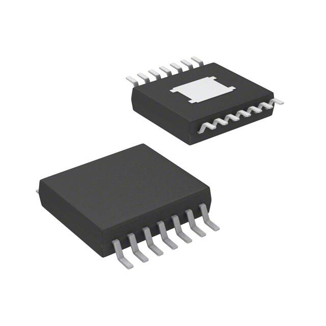
selection. The HTSSOP-14 (PWP) package
enhances the thermal performance of the LM2853.
1
•
•
•
•
•
•
•
•
Input Voltage Range of 3 V to 5.5 V
Factory EEPROM Set Output Voltages From
0.8 V to 3.3 V in 100 mV Increments
Maximum Load Current of 3A
Voltage Mode Control
Internal Type-Three Compensation
Switching Frequency of 550 kHz
Low Standby Current of 12 µA
Internal 40 mΩ MOSFET Switches
Standard Voltage Options
– 0.8/1.0/1.2/1.5/1.8/2.5/3.0/3.3 Volts
Exposed Pad 14-Lead HTSSOP (PWP) Package
2 Applications
•
•
•
Low Voltage Point of Load Regulation
Local Solution for FPGA/DSP/ASIC Core Power
Broadband Networking and Communications
Infrastructure
Typical Application Circuit
Device Information(1)
PART NUMBER
LM2853
PACKAGE
HTSSOP (14)
BODY SIZE (NOM)
5.00 mm × 4.40 mm
(1) For all available packages, see the orderable addendum at
the end of the data sheet.
Efficiency vs ILOAD
1
An IMPORTANT NOTICE at the end of this data sheet addresses availability, warranty, changes, use in safety-critical applications,
intellectual property matters and other important disclaimers. PRODUCTION DATA.
�LM2853
SNVS459A – OCTOBER 2006 – REVISED SEPTEMBER 2017
www.ti.com
Table of Contents
1
2
3
4
5
6
7
Features ..................................................................
Applications ...........................................................
Description .............................................................
Revision History.....................................................
Pin Configuration and Functions .........................
Specifications.........................................................
1
1
1
2
3
4
6.1
6.2
6.3
6.4
6.5
6.6
4
4
4
4
5
6
Absolute Maximum Ratings ......................................
ESD Ratings ............................................................
Recommended Operating Conditions.......................
Thermal Information ..................................................
Electrical Characteristics...........................................
Typical Characteristics ..............................................
Detailed Description .............................................. 8
7.1 Overview ................................................................... 8
7.2 Functional Block Diagram ......................................... 8
8
Application and Implementation .......................... 9
8.1 Application Information.............................................. 9
8.2 Typical Application .................................................. 13
9
Layout ................................................................... 14
9.1 Layout Guidelines ................................................... 14
9.2 Example Circuit Schematic and Bill of Materials .... 14
10 Device and Documentation Support ................. 16
10.1
10.2
10.3
10.4
10.5
Receiving Notification of Documentation Updates
Community Resources..........................................
Trademarks ...........................................................
Electrostatic Discharge Caution ............................
Glossary ................................................................
16
16
16
16
16
11 Mechanical, Packaging, and Orderable
Information ........................................................... 16
4 Revision History
Changes from Original (October 2006) to Revision A
Page
•
Added Application and Implementation section, Device Information table, Pin Configuration and Functions section,
ESD Ratings table, Thermal Information table, Device and Documentation Support section, and Mechanical,
Packaging, and Orderable Information section. ..................................................................................................................... 1
•
Changed layout of Data Sheet to TI format ........................................................................................................................... 1
2
Submit Documentation Feedback
Copyright © 2006–2017, Texas Instruments Incorporated
Product Folder Links: LM2853
�LM2853
www.ti.com
SNVS459A – OCTOBER 2006 – REVISED SEPTEMBER 2017
5 Pin Configuration and Functions
PWP
14-HTSSOP
Top View
Pin Functions
NO.
NAME
1
AVIN
DESCRIPTION
Input Voltage for Control Circuitry
2
EN
3
SGND
4
SS
Soft-Start Pin
No Connect. This pin must be tied to ground.
5
NC
6,7
PVIN
8,9
SW
10,11
PGND
12,13
NC
14
SNS
Exposed Pad
EP
Enable
Low noise ground
Input Voltage for Power Circuitry
Switch Pin
Power Ground
No-Connect. These pins must be tied to ground.
Output Voltage Sense Pin
The exposed pad is internally connected to GND, but it cannot be used as the primary GND
connection. The exposed pad should be soldered to an external GND plane.
Submit Documentation Feedback
Copyright © 2006–2017, Texas Instruments Incorporated
Product Folder Links: LM2853
3
�LM2853
SNVS459A – OCTOBER 2006 – REVISED SEPTEMBER 2017
www.ti.com
6 Specifications
6.1 Absolute Maximum Ratings
over operating free-air temperature range (unless otherwise noted) (1)
AVIN, PVIN, EN, SNS, SW, SS
MIN
MAX
UNIT
–0.3
6
V
Power Dissipation
14-Pin Exposed Pad HTSSOP Package (PWP)
Internally Limited
V
Infrared (15 sec)
220
°C
Vapor Phase (60 sec)
215
°C
Soldering (10 sec)
260
°C
150
°C
150
°C
Maximum junction temperature
Storage temperature, Tstg
(1)
–65
Stresses beyond those listed under Absolute Maximum Ratings may cause permanent damage to the device. These are stress ratings
only, which do not imply functional operation of the device at these or any other conditions beyond those indicated under Recommended
Operating Conditions. Exposure to absolute-maximum-rated conditions for extended periods may affect device reliability.
6.2 ESD Ratings
V(ESD)
(1)
Electrostatic discharge
VALUE
UNIT
±2
kV
Human-body model (HBM), per ANSI/ESDA/JEDEC JS-001 (1)
JEDEC document JEP155 states that 500-V HBM allows safe manufacturing with a standard ESD control process.
6.3 Recommended Operating Conditions
over operating free-air temperature range (unless otherwise noted)
(1)
PVIN to GND
AVIN to GND
Operation junction temperature, TJ
(1)
MIN
MAX
1.5
5.5
UNIT
V
3
5.5
V
–40
125
°C
Absolute maximum ratings indicate limits beyond which damage to the device may occur. Operating Range indicates conditions for
which the device is intended to be functional, but does not ensure specific performance limits. For ensured specifications and test
conditions, see the Electrical Characteristics.
6.4 Thermal Information
LM2853
THERMAL METRIC (1)
PWP (HTSSOP)
UNIT
14 PINS
RθJA
(1)
4
Junction-to-ambient thermal resistance
38
°C/W
For more information about traditional and new thermal metrics, see the Semiconductor and IC Package Thermal Metrics application
report.
Submit Documentation Feedback
Copyright © 2006–2017, Texas Instruments Incorporated
Product Folder Links: LM2853
�LM2853
www.ti.com
SNVS459A – OCTOBER 2006 – REVISED SEPTEMBER 2017
6.5 Electrical Characteristics
Specifications with standard typeface are for TJ = 25°C. Minimum and Maximum limits are ensured through test, design or
statistical correlation. Typical values represent the most likely parametric norm at TJ = 25°C and are provided for reference
purposes only. Unless otherwise specified AVIN = PVIN = 5 V.
PARAMETER
TEST CONDITIONS
MIN
TYP
MAX
0.8
0.818
1.0225
UNIT
SYSTEM PARAMETERS
VOUT
ΔVOUT/ΔA
VIN
ΔVOUT/ΔIO
Voltage tolerance
Line regulation
(1)
(1)
Load regulation
VOUT = 0.8 V option
TJ = –40°C to 125°C
0.782
VOUT = 1 V option
TJ = –40°C to 125°C
0.9775
1
VOUT = 1.2 V option
TJ = –40°C to 125°C
1.1730
1.2
1.227
VOUT = 1.5 V option
TJ = –40°C to 125°C
1.4663
1.5
1.5337
VOUT = 1.8 V option
TJ = –40°C to 125°C
1.7595
1.8
1.8405
VOUT = 2.5 V option
TJ = –40°C to 125°C
2.4437
2.5
2.5563
VOUT = 3 V option
TJ = –40°C to 125°C
2.9325
3
3.0675
VOUT = 3.3 V option
TJ = –40°C to 125°C
3.2257
3.3
3.3743
VOUT = 0.8 V, 1 V, 1.2 V, 1.5 V,
1.8 V or 2.5 V
3 V ≤ AVIN ≤ 5.5 V
TJ = –40°C to 125°C
0.2
1.1
%
VOUT = 3 V or 3.3 V
3.5 V ≤ AVIN ≤ 5.5 V
TJ = –40°C to 125°C
0.2
1.1
%
Rising
TJ = –40°C to 125°C
2.47
3
Normal operation
2
V
mV/A
V
VON
UVLO Threshold (AVIN)
Falling hysteresis
TJ = –40°C to 125°C
155
260
mV
RDS(ON)-P
PFET On resistance
Isw = 3A
TJ = –40°C to 125°C
40
120
mΩ
RDS(ON)-N
NFET On resistance
Isw = 3A
TJ = –40°C to 125°C
32
100
mΩ
RSS
Soft-Start resistance
ICL
Peak current limit
threshold
IQ
Operating current
Non-switching
TJ = –40°C to 125°C
0.85
2
mA
ISD
Shutdown quiescent
current
EN = 0 V
TJ = –40°C to 125°C
12
50
µA
RSNS
Sense pin resistance
50
3.6
450
kΩ
5
A
432
kΩ
PWM
fosc
Switching frequency
Drange
Duty cycle range
ENABLE CONTROL
.
TJ = –40°C to 125°C
325
TJ = –40°C to 125°C
0
75
550
725
kHz
100
%
(2)
VIH
EN Pin minimum high
input
TJ = –40°C to 125°C
VIL
EN Pin maximum low
input
TJ = –40°C to 125°C
IEN
EN Pin pullup current
EN = 0 V
% of
AVIN
25
% of
AVIN
1.5
µA
THERMAL CONTROLS
TSD
Thermal shutdown
threshold
165
°C
TSD-HYS
Hysteresis for thermal
shutdown
10
°C
(1)
(2)
VOUT measured in a non-switching, closed-loop configuration at the SNS pin.
The enable pin is internally pulled up, so the LM2853 is automatically enabled unless an external enable voltage is applied.
Submit Documentation Feedback
Copyright © 2006–2017, Texas Instruments Incorporated
Product Folder Links: LM2853
5
�LM2853
SNVS459A – OCTOBER 2006 – REVISED SEPTEMBER 2017
www.ti.com
6.6 Typical Characteristics
VOUT = 1.8 V
Figure 1. Efficiency vs ILOAD
Figure 2. NFET RDS(ON) vs Temperature
VOUT = 2.5 V
Figure 3. Efficiency vs ILOAD
6
Figure 4. PFET RDS(ON) vs Temperature
Submit Documentation Feedback
Copyright © 2006–2017, Texas Instruments Incorporated
Product Folder Links: LM2853
�LM2853
www.ti.com
SNVS459A – OCTOBER 2006 – REVISED SEPTEMBER 2017
Typical Characteristics (continued)
VOUT = 3.3 V
Figure 5. Efficiency vs ILOAD
Figure 6. Switching Frequency vs Temperature
Figure 7. IQ vs VIN and Temperature
Figure 8. ISD vs VIN and Temperature
Submit Documentation Feedback
Copyright © 2006–2017, Texas Instruments Incorporated
Product Folder Links: LM2853
7
�LM2853
SNVS459A – OCTOBER 2006 – REVISED SEPTEMBER 2017
www.ti.com
7 Detailed Description
7.1 Overview
The LM2853 is a DC-DC buck regulator belonging to Texas Instrument’s synchronous family. Integration of the
PWM controller, power switches and compensation network greatly reduces the component count required to
implement a switching power supply. A typical application requires only four components: an input capacitor, a
soft-start capacitor, an output filter capacitor and an output filter inductor.
7.2 Functional Block Diagram
8
Submit Documentation Feedback
Copyright © 2006–2017, Texas Instruments Incorporated
Product Folder Links: LM2853
�LM2853
www.ti.com
SNVS459A – OCTOBER 2006 – REVISED SEPTEMBER 2017
8 Application and Implementation
NOTE
Information in the following applications sections is not part of the TI component
specification, and TI does not warrant its accuracy or completeness. TI’s customers are
responsible for determining suitability of components for their purposes. Customers should
validate and test their design implementation to confirm system functionality.
8.1 Application Information
8.1.1 Input Capacitor (CIN)
Fast switching of large currents in the buck converter places a heavy demand on the voltage source supplying
PVIN. The input capacitor, CIN, supplies extra charge when the switcher needs to draw a burst of current from
the supply. The RMS current rating and the voltage rating of the CIN capacitor are therefore important in the
selection of CIN. The RMS current specification can be approximated by:
(1)
where D is the duty cycle, VOUT/VIN. CIN also provides filtering of the supply. Trace resistance and inductance
degrade the benefits of the input capacitor, so CIN should be placed very close to PVIN in the layout. A 22 µF or
47 µF ceramic capacitor is typically sufficient for CIN. In parallel with the large input capacitance a smaller
capacitor should be added such as a 1 µF ceramic for higher frequency filtering. Ceramic capacitors with high
quality dielectrics such as X5R or X7R should be used to provide a constant capacitance across temperature and
line variations. For improved load regulation and transient performance, the use of a small 1 µF ceramic
capacitor is also recommended as a local bypass for the AVIN pin.
8.1.2 Soft-Start Capacitor (CSS)
The DAC that sets the reference voltage of the error amplifier sources a current through a resistor to set the
reference voltage. The reference voltage is one half of the output voltage of the switcher due to the 200 kΩ
divider connected to the SNS pin. Upon start-up, the output voltage of the switcher tracks the reference voltage
with a two to one ratio as the DAC current charges the capacitance connected to the reference voltage node.
Internal capacitance of 20 pF is permanently attached to the reference voltage node which is also connected to
the soft start pin, SS. Adding a soft-start capacitor externally increases the time it takes for the output voltage to
reach its final level. The charging time required for the reference voltage can be estimated using the RC time
constant of the DAC resistor and the capacitance connected to the SS pin. Three RC time constant periods are
needed for the reference voltage to reach 95% of its final value. The actual start up time will vary with differences
in the DAC resistance and higher-order effects.
If little or no soft-start capacitance is connected, then the start up time may be determined by the time required
for the current limit current to charge the output filter capacitance. The capacitor charging equation I = CΔV/Δt
can be used to estimate the start-up time in this case. For example, a part with a 3 V output, a 100 μF output
capacitance and a 5A current limit threshold would require a time of 60 µs:
(2)
Since it is undesirable for the power supply to start up in current limit, a soft-start capacitor must be chosen to
force the LM2853 to start up in a more controlled fashion based on the charging of the soft-start capacitance. In
this example, suppose a 3 ms start time is desired. Three time constants are required for charging the soft-start
capacitor to 95% of the final reference voltage. So in this case RC = 1 ms. The DAC resistor, R, is 450 kΩ so C
can be calculated to be 2.2 nF. A 2.2 nF ceramic capacitor can be chosen to yield approximately a 3 ms start-up
time.
Submit Documentation Feedback
Copyright © 2006–2017, Texas Instruments Incorporated
Product Folder Links: LM2853
9
�LM2853
SNVS459A – OCTOBER 2006 – REVISED SEPTEMBER 2017
www.ti.com
Application Information (continued)
8.1.3 Soft-Start Capacitor (CSS) and Fault Conditions
Various fault conditions such as short circuit and UVLO of the LM2853 activate internal circuitry designed to
control the voltage on the soft-start capacitor. For example, during a short circuit current limit event, the output
voltage typically falls to a low voltage. During this time, the soft-start voltage is forced to track the output so that
once the short is removed, the LM2853 can restart gracefully from whatever voltage the output reached during
the short circuit event. The range of soft-start capacitors is therefore restricted to values 1 nF to 50 nF.
8.1.4 Compensation
The LM2853 provides a highly integrated solution to power supply design. The compensation of the LM2853,
which is type-three, is included on-chip. The benefit of integrated compensation is straight-forward, simple power
supply design. Since the output filter capacitor and inductor values impact the compensation of the control loop,
the range of LO, CO and CESR values is restricted in order to ensure stability.
8.1.5 Output Filter Values
Table 1 details the recommended inductor and capacitor ranges for the LM2853 that are suggested for various
typical output voltages. Values slightly different than those recommended may be used, however the phase
margin of the power supply may be degraded. For best performance when output voltage ripple is a concern,
ESR values near the minimum of the recommended range should be paired with capacitance values near the
maximum. If a minimum output voltage ripple solution from a 5 V input voltage is desired, a 6.8 μH inductor can
be paired with a 220 μF (50 mΩ) capacitor without degraded phase margin.
Table 1. Recommended LO and CO Values
VOUT (V)
0.8
1
1.2
1.5
1.8
2.5
3.0
3.3
VIN (V)
LO (µH)
CO (µF)
CESR (mΩ)
MIN
MAX
MIN
MAX
MIN
MAX
5
4.7
6.8
120
220
70
100
3.3
4.7
4.7
150
220
50
100
5
4.7
6.8
120
220
70
100
3.3
4.7
4.7
150
220
50
100
5
4.7
6.8
120
220
70
100
3.3
4.7
4.7
120
220
60
100
5
4.7
6.8
120
220
70
100
3.3
4.7
4.7
120
220
60
100
5
4.7
6.8
120
220
70
120
3.3
4.7
4.7
100
220
70
120
5
4.7
6.8
120
220
70
150
3.3
4.7
4.7
100
220
80
150
5
4.7
6.8
120
220
70
150
3.3
4.7
4.7
100
220
80
150
5
4.7
6.8
120
220
70
150
8.1.6 Choosing an Inductance Value
The current ripple present in the output filter inductor is determined by the input voltage, output voltage, switching
frequency and inductance according to Equation 3.
(3)
10
Submit Documentation Feedback
Copyright © 2006–2017, Texas Instruments Incorporated
Product Folder Links: LM2853
�LM2853
www.ti.com
SNVS459A – OCTOBER 2006 – REVISED SEPTEMBER 2017
where ΔIL is the peak to peak current ripple, D is the duty cycle VOUT/VIN, VIN is the input voltage applied to the
output stage, VOUT is the output voltage of the switcher, f is the switching frequency and LO is the inductance of
the output filter inductor. Knowing the current ripple is important for inductor selection since the peak current
through the inductor is the load current plus one half the ripple current. Care must be taken to ensure the peak
inductor current does not reach a level high enough to trip the current limit circuitry of the LM2853. As an
example, consider a 5 V to 1.2 V conversion and a 550 kHz switching frequency. According to Table 1, a 4.7 µH
inductor may be used. Calculating the expected peak-to-peak ripple,
(4)
The maximum inductor current for a 3A load would therefore be 3A plus 177 mA, 3.177A. As shown in the ripple
equation (Equation 4), the current ripple is inversely proportional to inductance.
8.1.7 Output Filter Inductors
Once the inductance value is chosen, the key parameter for selecting the output filter inductor is its saturation
current (ISAT) specification. Typically ISAT is given by the manufacturer as the current at which the inductance of
the coil falls to a certain percentage of the nominal inductance. The ISAT of an inductor used in an application
should be greater than the maximum expected inductor current to avoid saturation. Table 2 lists inductors that
are suitable in LM2853 applications.
Table 2. Recommended Inductors
INDUCTANCE
PART NUMBER
VENDOR
4.7 μF
DO3308P-472ML
Coilcraft
4.7 μF
DO3316P-472ML
Coilcraft
4.7 μF
MSS1260-472ML
Coilcraft
5.2 μF
MSS1038-522NL
Coilcraft
5.6 μF
MSS1260-562ML
Coilcraft
6.8 μF
DO3316P-682ML
Coilcraft
6.8 μF
MSS1260-682ML
Coilcraft
8.1.8 Output Filter Capacitors
The recommended capacitors that may be used in the output filter with the LM2853 are limited in value and ESR
range according to Table 1.
Table 3 shows some examples of capacitors that can typically be used in a LM2853 application.
Table 3. Recommended Capacitors
CAPACITANCE
(µF)
PART NUMBER
CHEMISTRY
VENDOR
100
594D107X_010C2T
Tantalum
Vishay-Sprague
100
593D107X_010D2_E3
Tantalum
Vishay-Sprague
100
TPSC107M006#0075
Tantalum
AVX
100
NOSD107M006#0080
Niobium Oxide
AVX
100
NOSC107M004#0070
Niobium Oxide
AVX
120
594D127X_6R3C2T
Tantalum
Vishay-Sprague
150
594D157X_010C2T
Tantalum
Vishay-Sprague
150
595D157X_010D2T
Tantalum
Vishay-Sprague
150
591D157X_6R3C2_20H
Tantalum
Vishay-Sprague
150
TPSD157M006#0050
Tantalum
AVX
150
TPSC157M004#0070
Tantalum
AVX
150
NOSD157M006#0070
Niobium Oxide
AVX
220
594D227X_6R3D2T
Tantalum
Vishay-Sprague
Submit Documentation Feedback
Copyright © 2006–2017, Texas Instruments Incorporated
Product Folder Links: LM2853
11
�LM2853
SNVS459A – OCTOBER 2006 – REVISED SEPTEMBER 2017
www.ti.com
Table 3. Recommended Capacitors (continued)
12
CAPACITANCE
(µF)
PART NUMBER
CHEMISTRY
VENDOR
220
591D227X_6R3D2_20H
Tantalum
Vishay-Sprague
220
591D227X_010D2_20H
Tantalum
Vishay-Sprague
220
593D227X_6R3D2_E3
Tantalum
Vishay-Sprague
220
TPSD227M006#0050
Tantalum
AVX
220
NOSD227M0040060
Niobium Oxide
AVX
Submit Documentation Feedback
Copyright © 2006–2017, Texas Instruments Incorporated
Product Folder Links: LM2853
�LM2853
www.ti.com
SNVS459A – OCTOBER 2006 – REVISED SEPTEMBER 2017
8.1.9 Split-Rail Operation
The LM2853 can be powered using two separate voltages for AVIN and PVIN. AVIN is the supply for the control
logic; PVIN is the supply for the power FETs. The output filter components need to be chosen based on the
value of PVIN. For PVIN levels lower than 3.3 V, use output filter component values recommended for 3.3 V.
PVIN must always be equal to or less than AVIN.
Figure 9. Split-Rail Operation Example Circuit
8.1.10 Switch Node Protection
The LM2853 includes protection circuitry that monitors the voltage on the switch pin. Under certain fault
conditions, switching is disabled in order to protect the switching devices. One side effect of the protection
circuitry may be observed when power to the LM2853 is applied with no or light load on the output. The output
will regulate to the rated voltage, but no switching may be observed. As soon as the output is loaded, the
LM2853 will begin normal switching operation.
8.2 Typical Application
Figure 10. LM2853 Typical Application Circuit
Submit Documentation Feedback
Copyright © 2006–2017, Texas Instruments Incorporated
Product Folder Links: LM2853
13
�LM2853
SNVS459A – OCTOBER 2006 – REVISED SEPTEMBER 2017
www.ti.com
9 Layout
9.1 Layout Guidelines
These are several guidelines to follow while designing the PCB layout for an LM2853 application.
1. The input bulk capacitor, CIN, should be placed very close to the PVIN pin to keep the resistance as low as
possible between the capacitor and the pin. High current levels will be present in this connection.
2. All ground connections must be tied together. Use a broad ground plane, for example a completely filled
back plane, to establish the lowest resistance possible between all ground connections.
3. The sense pin connection should be made as close to the load as possible so that the voltage at the load is
the expected regulated value. The sense line should not run too close to nodes with high dV/dt or dl/dt (such
as the switch node) to minimize interference.
4. The switch node connections should be low resistance to reduce power losses. Low resistance means the
trace between the switch pin and the inductor should be wide. However, the area of the switch node should
not be too large since EMI increases with greater area. So connect the inductor to the switch pin with a short,
but wide trace. Other high current connections in the application such as PVIN and VOUT assume the same
trade off between low resistance and EMI.
5. Allow area under the chip to solder the entire exposed die attach pad to ground for improved thermal
performance. Lab measurements also show improved regulation performance when the exposed pad is well
grounded.
9.2 Example Circuit Schematic and Bill of Materials
Figure 11. LM2853 Example Circuit Schematic
Table 4. Bill of Materials for 5 V to 3.3 V Conversion
ID
PART NUMBER
TYPE
SIZE
PARAMETERS
QTY
U1
LM2853MH-3.3
3A Buck
HTSSOP-14
3.3 V
1
VENDOR
TI
CIN
GRM31CR60J476ME19
Capacitor
1206
47 µF
1
Murata
CBYP
GRM21BR71C105KA01
Capacitor
0805
1 µF
1
Murata
CSS
VJ0805Y222KXXA
Capacitor
0603
2.2 nF
1
Vishay-Vitramon
LO
DO3316P-682
Inductor
DO3316P
6.8 µH
1
Coilcraft
CO
594D127X06R3C2T
Capacitor
C Case
120 μF (85 mΩ)
1
Vishay-Sprague
Table 5. Bill of Materials for 3.3 V to 1.2 V Conversion
14
ID
PART NUMBER
TYPE
SIZE
PARAMETERS
QTY
VENDOR
U1
LM2853MH-1.2
3A Buck
HTSSOP-14
1.2 V
1
TI
Murata
CIN
GRM31CR60J476ME19
Capacitor
1206
47 µF
1
CBYP
GRM21BR71C105KA01
Capacitor
0805
1 µF
1
Murata
CSS
VJ0805Y222KXXA
Capacitor
0603
2.2 nF
1
Vishay-Vitramon
LO
DO3316P-472
Inductor
DO3316P
4.7 μH
1
Coilcraft
Submit Documentation Feedback
Copyright © 2006–2017, Texas Instruments Incorporated
Product Folder Links: LM2853
�LM2853
www.ti.com
SNVS459A – OCTOBER 2006 – REVISED SEPTEMBER 2017
Table 5. Bill of Materials for 3.3 V to 1.2 V Conversion (continued)
ID
PART NUMBER
TYPE
SIZE
PARAMETERS
QTY
VENDOR
CO
NOSD157M006R0070
Capacitor
D Case
150 μF (70 mΩ)
1
AVX
Submit Documentation Feedback
Copyright © 2006–2017, Texas Instruments Incorporated
Product Folder Links: LM2853
15
�LM2853
SNVS459A – OCTOBER 2006 – REVISED SEPTEMBER 2017
www.ti.com
10 Device and Documentation Support
10.1 Receiving Notification of Documentation Updates
To receive notification of documentation updates, navigate to the device product folder on ti.com. In the upper
right corner, click on Alert me to register and receive a weekly digest of any product information that has
changed. For change details, review the revision history included in any revised document.
10.2 Community Resources
The following links connect to TI community resources. Linked contents are provided "AS IS" by the respective
contributors. They do not constitute TI specifications and do not necessarily reflect TI's views; see TI's Terms of
Use.
TI E2E™ Online Community TI's Engineer-to-Engineer (E2E) Community. Created to foster collaboration
among engineers. At e2e.ti.com, you can ask questions, share knowledge, explore ideas and help
solve problems with fellow engineers.
Design Support TI's Design Support Quickly find helpful E2E forums along with design support tools and
contact information for technical support.
10.3 Trademarks
E2E is a trademark of Texas Instruments.
All other trademarks are the property of their respective owners.
10.4 Electrostatic Discharge Caution
This integrated circuit can be damaged by ESD. Texas Instruments recommends that all integrated circuits be handled with
appropriate precautions. Failure to observe proper handling and installation procedures can cause damage.
ESD damage can range from subtle performance degradation to complete device failure. Precision integrated circuits may be more
susceptible to damage because very small parametric changes could cause the device not to meet its published specifications.
10.5 Glossary
SLYZ022 — TI Glossary.
This glossary lists and explains terms, acronyms, and definitions.
11 Mechanical, Packaging, and Orderable Information
The following pages include mechanical, packaging, and orderable information. This information is the most
current data available for the designated devices. This data is subject to change without notice and revision of
this document. For browser-based versions of this data sheet, refer to the left-hand navigation.
16
Submit Documentation Feedback
Copyright © 2006–2017, Texas Instruments Incorporated
Product Folder Links: LM2853
�PACKAGE OPTION ADDENDUM
www.ti.com
10-Dec-2020
PACKAGING INFORMATION
Orderable Device
Status
(1)
Package Type Package Pins Package
Drawing
Qty
Eco Plan
(2)
Lead finish/
Ball material
MSL Peak Temp
Op Temp (°C)
Device Marking
(3)
(4/5)
(6)
LM2853MH-1.0/NOPB
ACTIVE
HTSSOP
PWP
14
94
RoHS & Green
SN
Level-1-260C-UNLIM
-40 to 125
LM2853
-1.0
LM2853MH-1.2/NOPB
ACTIVE
HTSSOP
PWP
14
94
RoHS & Green
SN
Level-1-260C-UNLIM
-40 to 125
LM2853
-1.2
LM2853MH-1.5/NOPB
ACTIVE
HTSSOP
PWP
14
94
RoHS & Green
SN
Level-1-260C-UNLIM
-40 to 125
LM2853
-1.5
LM2853MH-1.8/NOPB
ACTIVE
HTSSOP
PWP
14
94
RoHS & Green
SN
Level-1-260C-UNLIM
-40 to 125
LM2853
-1.8
LM2853MH-2.5/NOPB
ACTIVE
HTSSOP
PWP
14
94
RoHS & Green
SN
Level-1-260C-UNLIM
-40 to 125
LM2853
-2.5
LM2853MH-3.0/NOPB
ACTIVE
HTSSOP
PWP
14
94
RoHS & Green
SN
Level-1-260C-UNLIM
-40 to 125
LM2853
-3.0
LM2853MH-3.3/NOPB
ACTIVE
HTSSOP
PWP
14
94
RoHS & Green
SN
Level-1-260C-UNLIM
-40 to 125
LM2853
-3.3
LM2853MHX-1.0/NOPB
ACTIVE
HTSSOP
PWP
14
2500
RoHS & Green
SN
Level-1-260C-UNLIM
-40 to 125
LM2853
-1.0
LM2853MHX-1.2/NOPB
ACTIVE
HTSSOP
PWP
14
2500
RoHS & Green
SN
Level-1-260C-UNLIM
-40 to 125
LM2853
-1.2
LM2853MHX-1.5/NOPB
ACTIVE
HTSSOP
PWP
14
2500
RoHS & Green
SN
Level-1-260C-UNLIM
-40 to 125
LM2853
-1.5
LM2853MHX-1.8/NOPB
ACTIVE
HTSSOP
PWP
14
2500
RoHS & Green
SN
Level-1-260C-UNLIM
-40 to 125
LM2853
-1.8
LM2853MHX-2.5/NOPB
ACTIVE
HTSSOP
PWP
14
2500
RoHS & Green
SN
Level-1-260C-UNLIM
-40 to 125
LM2853
-2.5
LM2853MHX-3.3/NOPB
ACTIVE
HTSSOP
PWP
14
2500
RoHS & Green
SN
Level-1-260C-UNLIM
-40 to 125
LM2853
-3.3
(1)
The marketing status values are defined as follows:
ACTIVE: Product device recommended for new designs.
LIFEBUY: TI has announced that the device will be discontinued, and a lifetime-buy period is in effect.
NRND: Not recommended for new designs. Device is in production to support existing customers, but TI does not recommend using this part in a new design.
PREVIEW: Device has been announced but is not in production. Samples may or may not be available.
OBSOLETE: TI has discontinued the production of the device.
Addendum-Page 1
Samples
�PACKAGE OPTION ADDENDUM
www.ti.com
10-Dec-2020
(2)
RoHS: TI defines "RoHS" to mean semiconductor products that are compliant with the current EU RoHS requirements for all 10 RoHS substances, including the requirement that RoHS substance
do not exceed 0.1% by weight in homogeneous materials. Where designed to be soldered at high temperatures, "RoHS" products are suitable for use in specified lead-free processes. TI may
reference these types of products as "Pb-Free".
RoHS Exempt: TI defines "RoHS Exempt" to mean products that contain lead but are compliant with EU RoHS pursuant to a specific EU RoHS exemption.
Green: TI defines "Green" to mean the content of Chlorine (Cl) and Bromine (Br) based flame retardants meet JS709B low halogen requirements of


 工商网监
湘ICP备2023018690号
工商网监
湘ICP备2023018690号
